

Page 1
SERVICE MANUAL
DVD RECORDER
ZC352MW8A
Page 2

IMPORTANT SAFETY NOTICE
Proper service and repair is important to the safe, reliable operation of all
Funai Equipment. The service procedures recommended by Funai and
described in this service manual are effecti ve methods of performing
service operations. Some of these service special tools should be used
when and as recommended.
It is important to note that this service manual contains various CA UTIONS
and NOTICES which should be carefully read in order to minimize the risk
of personal injury to service personnel. The possibility exists that improper
service methods may damage the equipment. It al so is important to
understand that these CA UTIONS and NOTICES ARE NOT EXHAUSTIVE.
Funai could not possibly know, evaluate and advice the service trade of all
conceivable ways in which service might be done or of the possible
hazardous consequences of each way. Consequently, Funai has not
undertaken any such broad evaluation. Accordingly, a servicer who uses a
service procedure or tool which is not recommended by Funai must first
use all precautions thoroughly so that neither his safety nor the safe
operation of the equipment will be jeopardized by the service method
selected.
TABLE OF CONTENTS
Specifications . . . . . . . . . . . . . . . . . . . . . . . . . . . . . . . . . . . . . . . . . . . . . . . . . . . . . . . . . . . . . . . . . . . . . . . . . .1-1-1
Laser Beam Safety Precautions . . . . . . . . . . . . . . . . . . . . . . . . . . . . . . . . . . . . . . . . . . . . . . . . . . . . . . . . . . . .1-2-1
Important Safety Precautions . . . . . . . . . . . . . . . . . . . . . . . . . . . . . . . . . . . . . . . . . . . . . . . . . . . . . . . . . . . . . .1-3-1
Standard Notes for Servicing . . . . . . . . . . . . . . . . . . . . . . . . . . . . . . . . . . . . . . . . . . . . . . . . . . . . . . . . . . . . . .1-4-1
Cabinet Disassembly Instructions. . . . . . . . . . . . . . . . . . . . . . . . . . . . . . . . . . . . . . . . . . . . . . . . . . . . . . . . . . .1-5-1
How to Initialize the DVD Recorder. . . . . . . . . . . . . . . . . . . . . . . . . . . . . . . . . . . . . . . . . . . . . . . . . . . . . . . . . .1-6-1
Firmware Renewal Mode . . . . . . . . . . . . . . . . . . . . . . . . . . . . . . . . . . . . . . . . . . . . . . . . . . . . . . . . . . . . . . . . .1-7-1
Function Indicator Symbols. . . . . . . . . . . . . . . . . . . . . . . . . . . . . . . . . . . . . . . . . . . . . . . . . . . . . . . . . . . . . . . .1-8-1
Block Diagrams. . . . . . . . . . . . . . . . . . . . . . . . . . . . . . . . . . . . . . . . . . . . . . . . . . . . . . . . . . . . . . . . . . . . . . . . .1-9-1
Schematic Diagrams / CBA’s . . . . . . . . . . . . . . . . . . . . . . . . . . . . . . . . . . . . . . . . . . . . . . . . . . . . . . . . . . . . .1-10-1
Waveforms . . . . . . . . . . . . . . . . . . . . . . . . . . . . . . . . . . . . . . . . . . . . . . . . . . . . . . . . . . . . . . . . . . . . . . . . . . .1-11-1
Wiring Diagram . . . . . . . . . . . . . . . . . . . . . . . . . . . . . . . . . . . . . . . . . . . . . . . . . . . . . . . . . . . . . . . . . . . . . . . .1-12-1
System Control Timing Charts . . . . . . . . . . . . . . . . . . . . . . . . . . . . . . . . . . . . . . . . . . . . . . . . . . . . . . . . . . . .1-13-1
IC Pin Function Descriptions. . . . . . . . . . . . . . . . . . . . . . . . . . . . . . . . . . . . . . . . . . . . . . . . . . . . . . . . . . . . . .1-14-1
Lead Identifications . . . . . . . . . . . . . . . . . . . . . . . . . . . . . . . . . . . . . . . . . . . . . . . . . . . . . . . . . . . . . . . . . . . . .1-15-1
Exploded Views. . . . . . . . . . . . . . . . . . . . . . . . . . . . . . . . . . . . . . . . . . . . . . . . . . . . . . . . . . . . . . . . . . . . . . . .1-16-1
Mechanical Parts List . . . . . . . . . . . . . . . . . . . . . . . . . . . . . . . . . . . . . . . . . . . . . . . . . . . . . . . . . . . . . . . . . . .1-17-1
Electrical Parts List . . . . . . . . . . . . . . . . . . . . . . . . . . . . . . . . . . . . . . . . . . . . . . . . . . . . . . . . . . . . . . . . . . . . .1-18-1
Manufactured under license from Dolby Laboratories.
“Dolby” and the double-D symbol are trademarks of Dolby Laboratories.
Page 3
SPECIFICATIONS
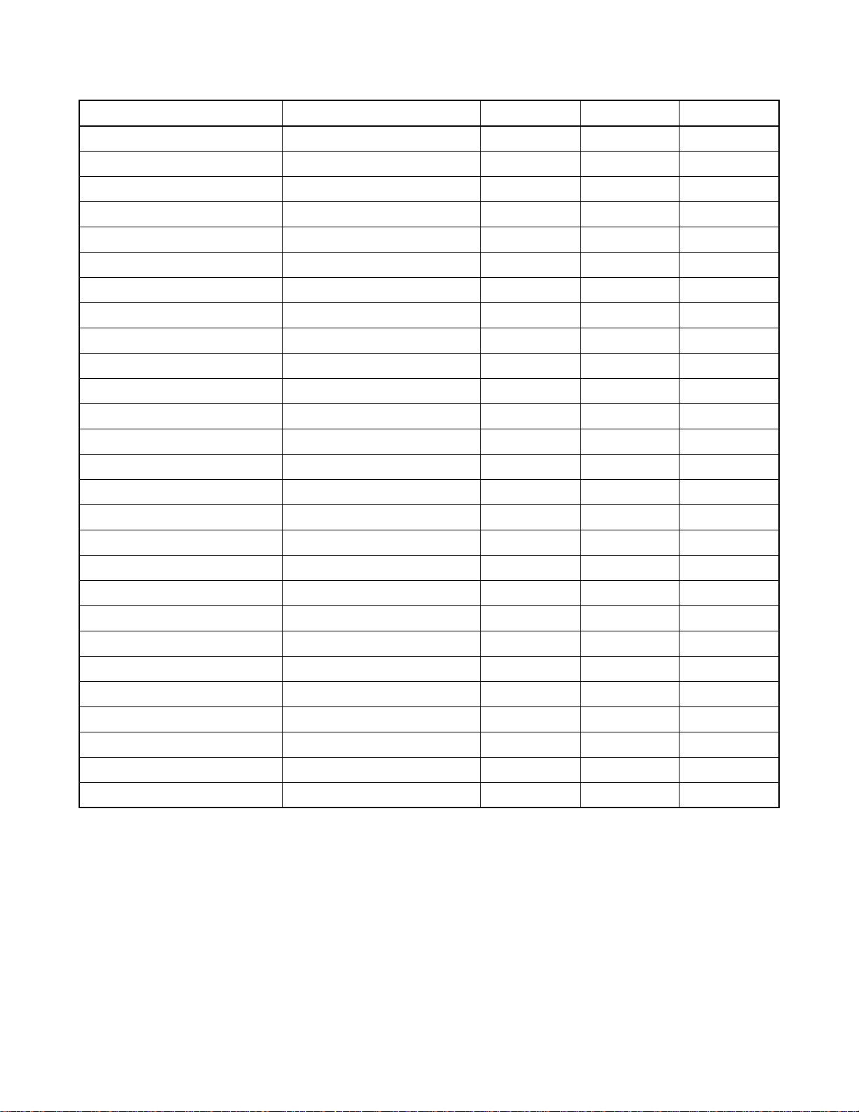
Item Conditions Unit Nominal Limit
1. VIDEO
1-1. Video Output 75 Ω load Vp-p 1.0
1-2. S-Video Output
Y (Luminance) 75 Ω load Vp-p 1.0
C (Chrominance) 75 Ω load Vp-p 0.286
1-3. Component Output
Y (Luminance) 75 Ω load Vp-p 1.0
Cb (U) 75 Ω load Vp-p 0.7
Cr (V) 75 Ω load Vp-p 0.7
2. AUDIO
2-1. Output Level Vrms 2.0
2-2. Frequency Response
DVD-VIDEO LPCM fs = 96 kHz Hz 20 - 44 k
fs = 48 kHz Hz 20 - 20 k
Audio CD fs = 44.1 kHz Hz 20 - 20 k
2-3. Signal/Noise Ratio
DVD-VIDEO LPCM A-Weight + SPCL20kHz dB 122
CD A-Weight + SPCL20kHz dB 122
REC & Playback Input: 2 Vrms, Rec Speed: XP dB 90
2-4. Dynamic Range
DVD-VIDEO LPCM dB 93
CD dB 93
REC & Playback Input: 2 Vrms, Rec Speed: XP dB 90
2-5. THD+N 1 kHz, 0 dB
DVD-VIDEO LPCM % 0.0035
CD % 0.004
REC & Playback Input: 2 Vrms, Rec Speed: XP % 0.0055
Notes:
1. All Items are measured without pre-emphasis unless otherwise specified.
2. Power supply: AC 120 V, 60 Hz
3. Load imp.: 100 kΩ
4. Room ambient: 5 °C ~ 40 °C
1-1-1 E7H50SP
Page 4
LASER BEAM SAFETY PRECAUTIONS
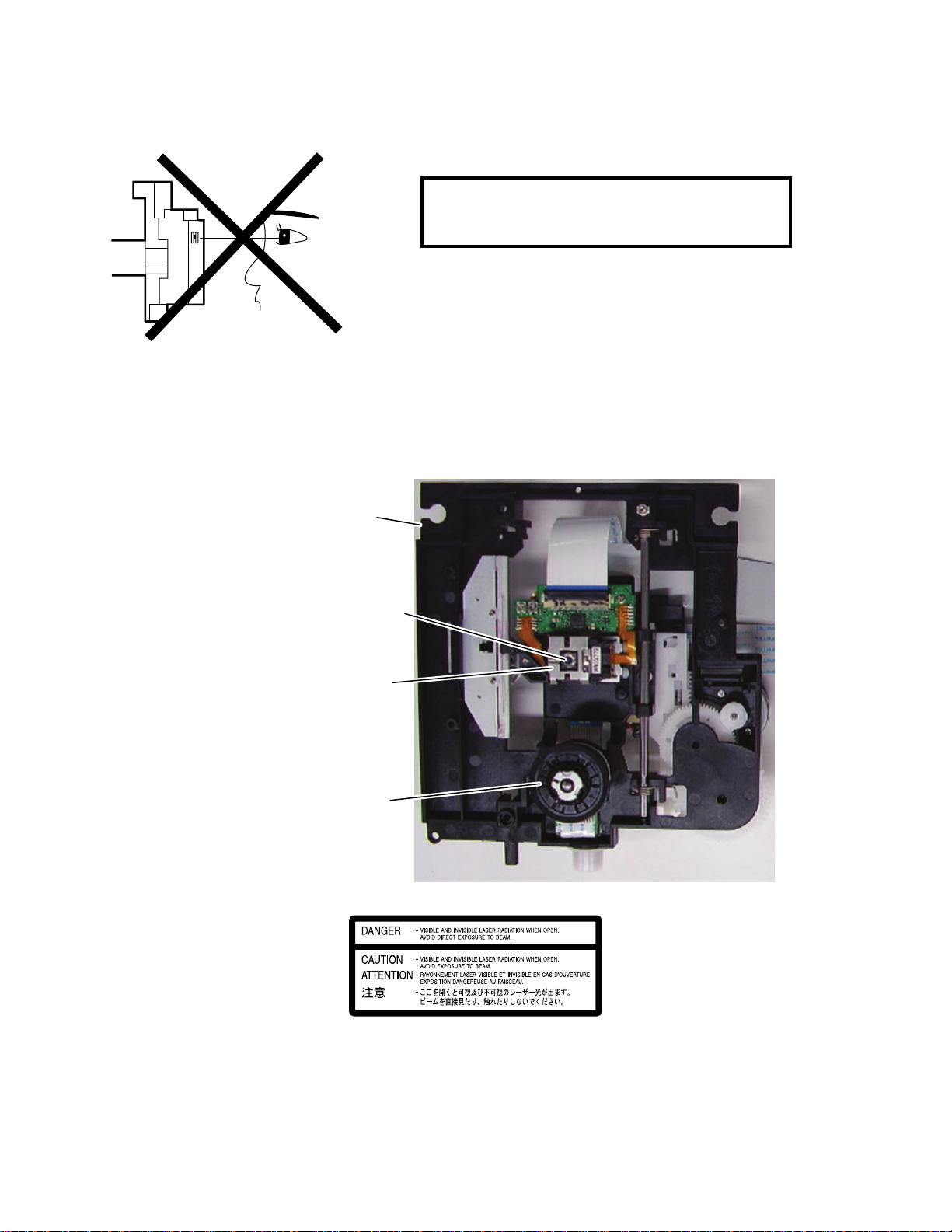
This DVD player uses a pickup that emits a laser beam.
Do not look directly at the laser beam coming
from the pic kup or allo w it to strike a gainst your
skin.
The laser beam is emitted from the location shown in the figure. When checking the laser diode, be sure to keep
your eyes at least 30 cm away from the pickup lens when the diode is turned on. Do not look directly at the laser
beam.
CAUTION: Use of controls and adjustments, or doing procedures other than those specified herein, may result in
hazardous radiation exposure.
Drive Mechanism Assembly
Laser Beam Radiation
Laser Pickup
Turntable
Location: Inside Top of DVD mechanism.
1-2-1 RL4NLSP
Page 5

IMPORTANT SAFETY PRECAUTIONS
Product Safety Notice
Some electrical and mechanical parts have special
safety -related characterist ics which are often not
evident from visual inspection, nor can the protection
they give necessarily be obtained by replacing them
with components rated for higher voltage, wattage,
etc. Parts that have special safety characteristics are
identified by a # on schematics and in parts lists. Use
of a substitute replacement that does not have the
same safety characteristics as the recommended
replaceme nt part might create shoc k, fire , and /or oth er
hazards. The Product’s Safety is under review
continuously and new instructions are issued
whenever appropriate. Prior to shipment from the
factory , our products are carefully inspected to confirm
with the recognized product safety and electrical
codes of the countries in which they are to be sold.
Howev e r, in order to maintain such compliance, it is
equally important to implement the following
precauti ons when a set is being serviced.
Precautions during Servicing
A. Parts identified by the # symbol are critical for
safety. Replace only with part number specified.
B. In addition to safety, other parts and assemblies
are specified for conformance with regulations
applying to spurious radiation. These must also be
replaced only with specified replacements.
Examples: RF converters, RF cables, noise
blocking capacitors, and noise blocking filters, etc.
C. Use specified internal wiring. Note especially:
1) Wires covered with PVC tubing
2) Double insulated wires
3) High voltage leads
D. Use specified insulating materials for hazardous
live parts. Note especiall y:
1) Insulation tape
2) PVC tubing
3) Spacers
4) Insulators for transistors
E. When replacing AC primary side components
(transformers, power cord, etc.), wrap ends of
wires securely about the terminals before
soldering.
F. Observe that the wires do not contact heat
producing parts (heat sinks, oxide metal film
resistors, fusible resistors, etc.).
G. Check that replaced wires do not contact sharp
edges or pointed parts.
H. When a power cord has been replaced, check that
5 - 6 kg of force in any direction will not loosen it.
I. Also check areas surrounding repaired locations.
J. Be careful that foreign objects (screws, solder
droplets, etc.) do not remain inside the set.
K. When connecting or disconnecting the internal
connectors, first, disconnect the AC plug from the
AC outlet.
1-3-1 DVDN_ISP
Page 6
Safety Check after Servici n g
Examine the area surrounding the repaired location for damage or deterioration. Observe that screws, parts, and
wires have been returned to their original positions. Afterwards, do the following tests and confirm the specified
values to verify compliance with safety standards.
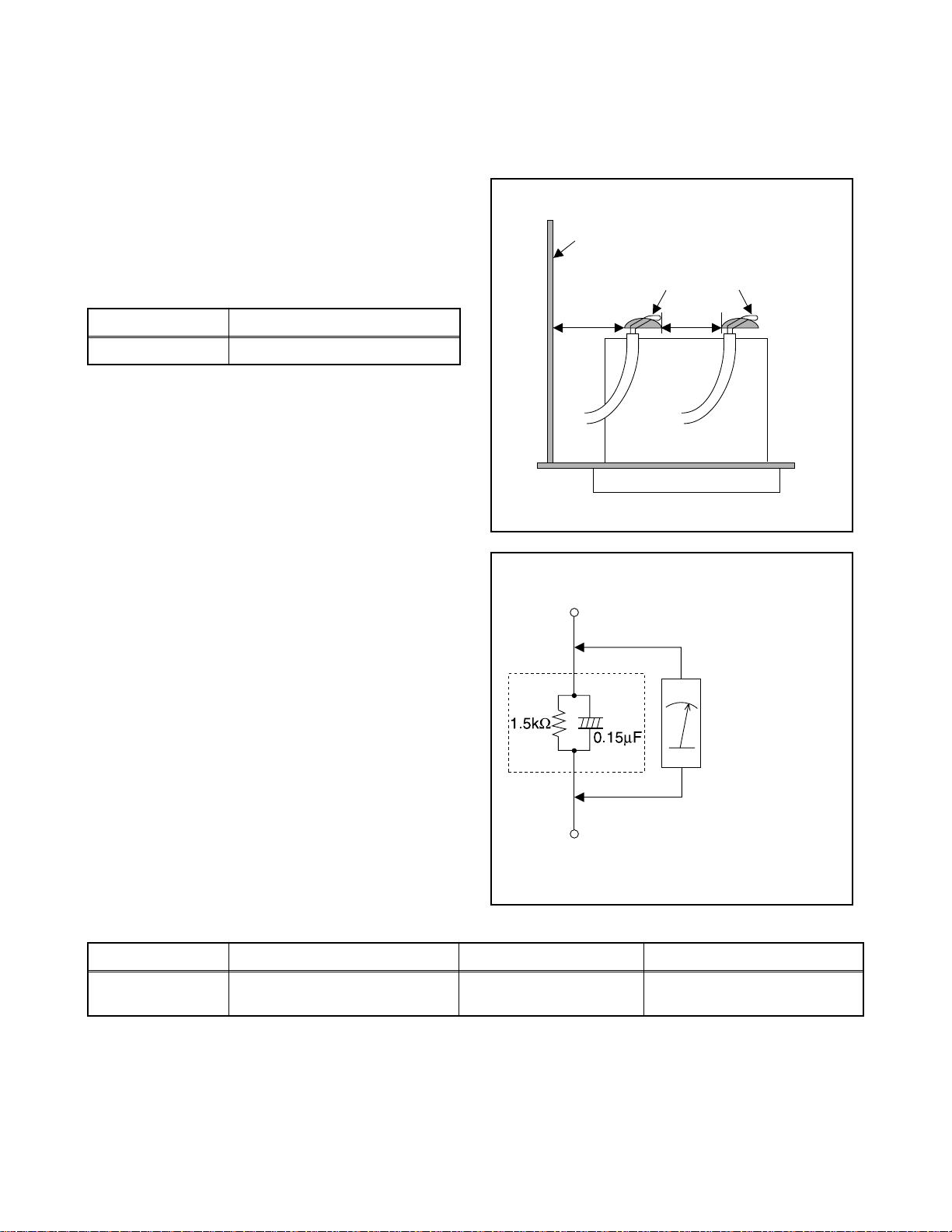
1. Clearance Distance
When replacing primary circuit components, confirm
specified clearance distance (d) and (d’) between
soldered terminals, and between terminals and
surrounding metallic parts. (See Fig. 1)
Table 1: Ratings for selected area
Chassis or Secondary Conductor
Primary Circuit
AC Line Voltage Clearance Distance (d), (d’)
120 V ≥ 3.2 mm (0.126 inches)
Note: This table is unofficial and for reference only. Be
sure to confirm the precise values.
2. Leakage Current Test
Confirm the specified (or lower) leakage current
between B (earth ground, power cord plug prongs) and
externally exposed accessible parts (RF terminals,
antenna terminals, video and audio input and output
terminals, microphone jacks, earphone jacks, etc.) is
lower than or equal to the specified value in the table
below.
Measuring Method (Power ON):
Insert load Z between B (earth ground, power cord plug
prongs) and exposed accessible parts. Use an AC
voltmeter to measure across the terminals of load Z.
See Fig. 2 and the following table.
d' d
Fig. 1
Exposed Accessible Part
Z
AC V oltmeter
(High Impedance)
Earth Ground
B
Power Cord Plug Prongs
Table 2: Leakage current ratings for selected areas
AC Line Voltage Load Z Leakage Current (i) Earth Ground (B) to:
120 V
Note: This table is unofficial and for reference only. Be sure to confirm the precise values.
0.15 µF CAP. & 1.5 kΩ RES.
Connected in parallel
i ≤ 0.5 mA Peak Exposed accessible parts
1-3-2 DVDN_ISP
Fig. 2
Page 7
STANDARD NOTES FOR SERVICIN G
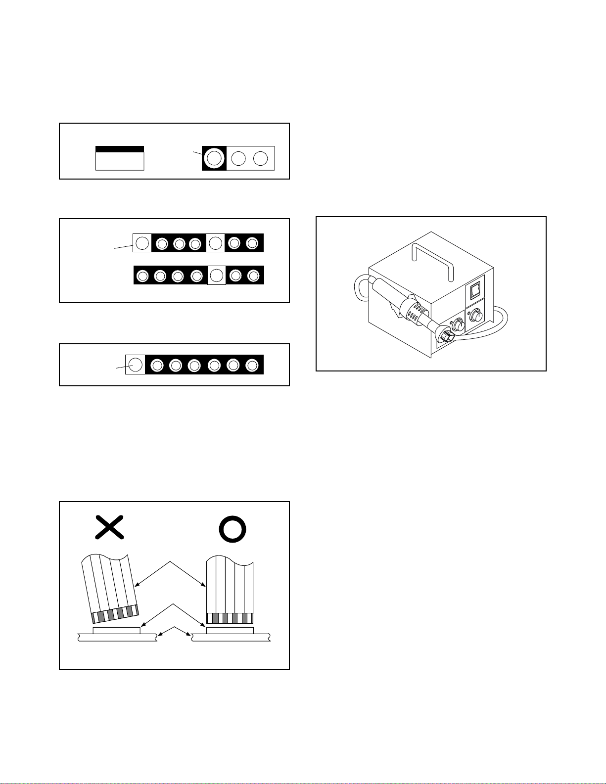
Circuit Board Indications
1. The output pin of the 3 pin Regulator ICs is
indicated as shown.
Top View
Out
2. For other ICs, pin 1 and every fifth pin are
indicated as shown.
Pin 1
3. The 1st pin of every male connector is indicated as
shown.
Pin 1
Input
In
Bottom View
5
10
Pb (Lead) Free Solder
When soldering, be sure to use the Pb free solder.
How to Remove / Install Flat Pack-IC
1. Removal
With Hot-Air Flat Pack-IC Desoldering Machine:
1. Prepare the hot-air flat pack-IC desoldering
machine, then apply hot air to the Flat Pack-IC
(about 5 to 6 seconds). (Fig. S-1-1)
Fig. S-1-1
Instructions for Connectors
1. When you connect or disconnect the FFC (Flexible
Foil Connector) cable, be sure to first disconnect
the AC cord.
2. FFC (Flexible Foil Connector) cable should be
inserted parallel into the connector, not at an
angle.
FFC Cable
Connector
CBA
* Be careful to avoid a short circuit.
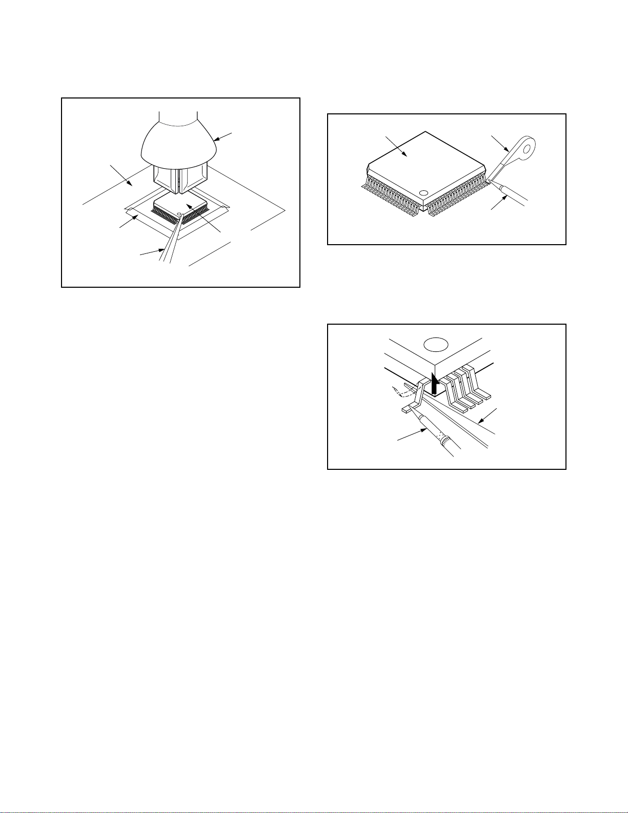
2. Remove the flat pack-IC with tweezers while
applying the hot air.
3. Bottom of the flat pack-IC is fixed with glue to the
CBA; when removing entire flat pack-IC, first apply
soldering iron to center of the flat pack-IC and heat
up. Then remove (glue will be melted). (Fig. S-1-6)
4. Release the flat pack-IC from the CBA using
tweezers. (Fig. S-1-6)
CAUTION:
1. The Fl at Pack-IC shape ma y dif f er by mode ls . U se
an appropriate hot-air flat pack-IC desoldering
machine, whose shape matches that of the Flat
Pack-IC.
2. Do not supply hot air to the chip parts around the
flat pack-IC for over 6 seconds because damage
to the chip parts may occur. Put masking tape
around the flat pack-IC to protect other parts from
damage. (Fig. S-1-2)
1-4-1 DVDN_SN
Page 8
3. The flat pack-IC on the CBA is affixed with glue, so
be careful not to break or damage the foil of each
pin or the solder lands under the IC when
removing it.
With Soldering Iron:
1. Using desoldering braid, remove the solder from
all pins of the flat pack-IC. When you use solder
flux which is applied to all pins of the flat pack-IC,
you can remove it easily. (Fig. S-1-3)
CBA
Masking
Tape
Tweezers
Hot-air
Flat Pack-IC
Desoldering
Machine
Flat Pack-IC
Fig. S-1-2
Flat Pack-IC
Desoldering Braid
Soldering Iron
Fig. S-1-3
2. Lift each lead of the flat pack-IC upward one by
one, using a sharp pin or wire to which solder will
not adhere (iron wire). When heating the pins, use
a fine tip soldering iron or a hot air desoldering
machine. (Fig. S-1-4)
Sharp
Pin
Fine Tip
Soldering Iron
3. Bottom of the flat pack-IC is fixed with glue to the
CBA; when removing entire flat pack-IC, first apply
soldering iron to center of the flat pack-IC and heat
up. Then remove (glue will be melted). (Fig. S-1-6)
4. Release the flat pack-IC from the CBA using
tweezers. (Fig. S-1-6)
Fig. S-1-4
1-4-2 DVDN_SN
Page 9
With Iron Wire:
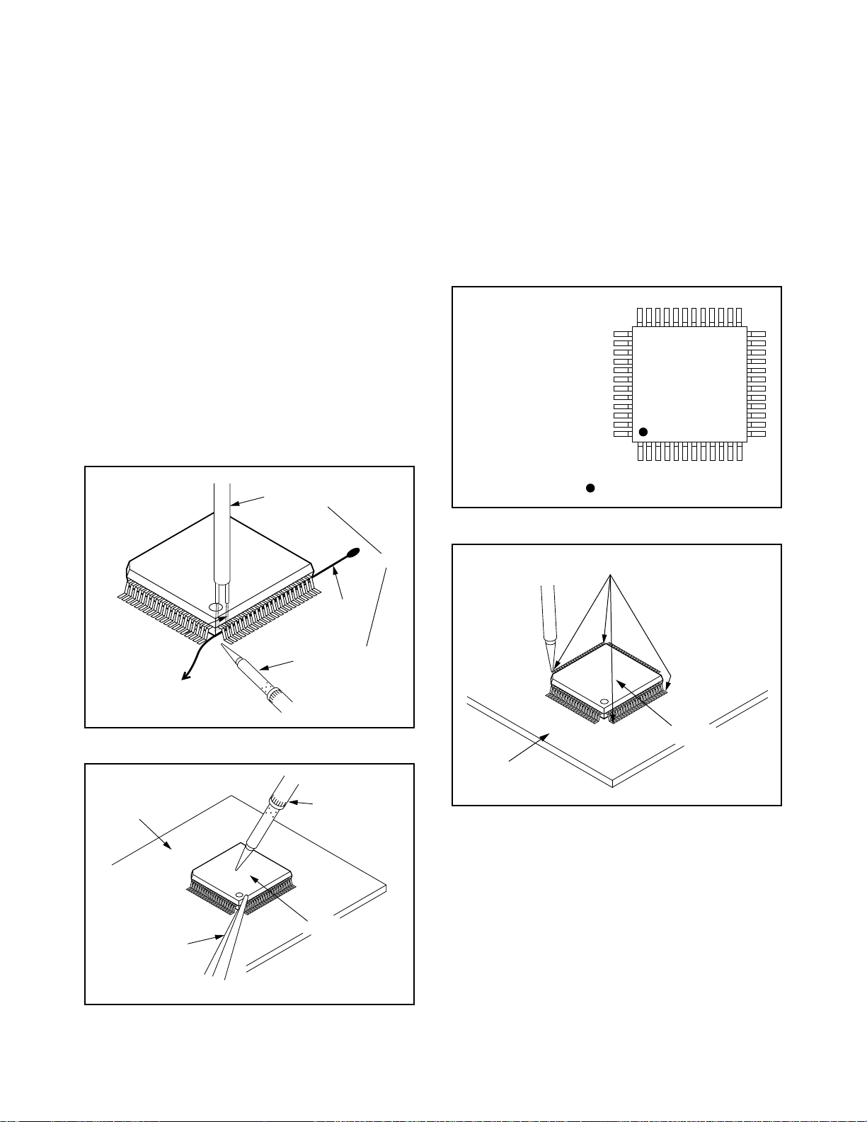
1. Using desoldering braid, remove the solder from
all pins of the flat pack-IC. When you use solder
flux which is applied to all pins of the flat pack-IC,
you can remove it easily. (Fig. S-1-3)
2. Affix the wire to a workbench or solid mounting
point, as shown in Fig. S-1-5.
3. While heating the pins using a fine tip soldering
iron or hot air blower, pull up the wire as the solder
melts so as to lift the IC leads from the CBA
contact pads as shown in Fig. S-1-5.
4. Bottom of the flat pack-IC is fixed with glue to the
CBA; when removing entire flat pack-IC, first apply
soldering iron to center of the flat pack-IC and heat
up. Then remove (glue will be melted). (Fig. S-1-6)
5. Release the flat pack-IC from the CBA using
tweezers. (Fig. S-1-6)
Note: When using a soldering iron, care must be
taken to ensure that the flat pack-IC is not
being held by glue. When the flat pack-IC is
removed from the CBA, handle it gently
because it may be damaged if force is applied.
Hot Air Blower
2. Installation
1. Using desoldering braid, remove the solder from
the foil of each pin of the flat pack-IC on the CBA
so you can install a replacement flat pack-IC more
easily.
2. The “●” mark on the flat pack-IC indicates pin 1.
(See Fig. S-1-7.) Be sure this mark matches the 1
on the PCB when positioning for installation. Then
presolder the four corners of the flat pack-IC. (See
Fig. S-1-8.)
3. Solder all pins of the flat pack-IC. Be sure that
none of the pins have solder bridges.
Example :
Pin 1 of the Flat Pack-IC
is indicated by a " " mark.
Fig. S-1-7
To Solid
Mounting Point
CBA
Tweezers
Iron Wire
Soldering Iron
Fig. S-1-5
Fine Tip
Soldering Iron
Flat Pack-IC
or
Presolder
Flat Pack-IC
CBA
Fig. S-1-8
Fig. S-1-6
1-4-3 DVDN_SN
Page 10
Instructions for Handling Semiconductors
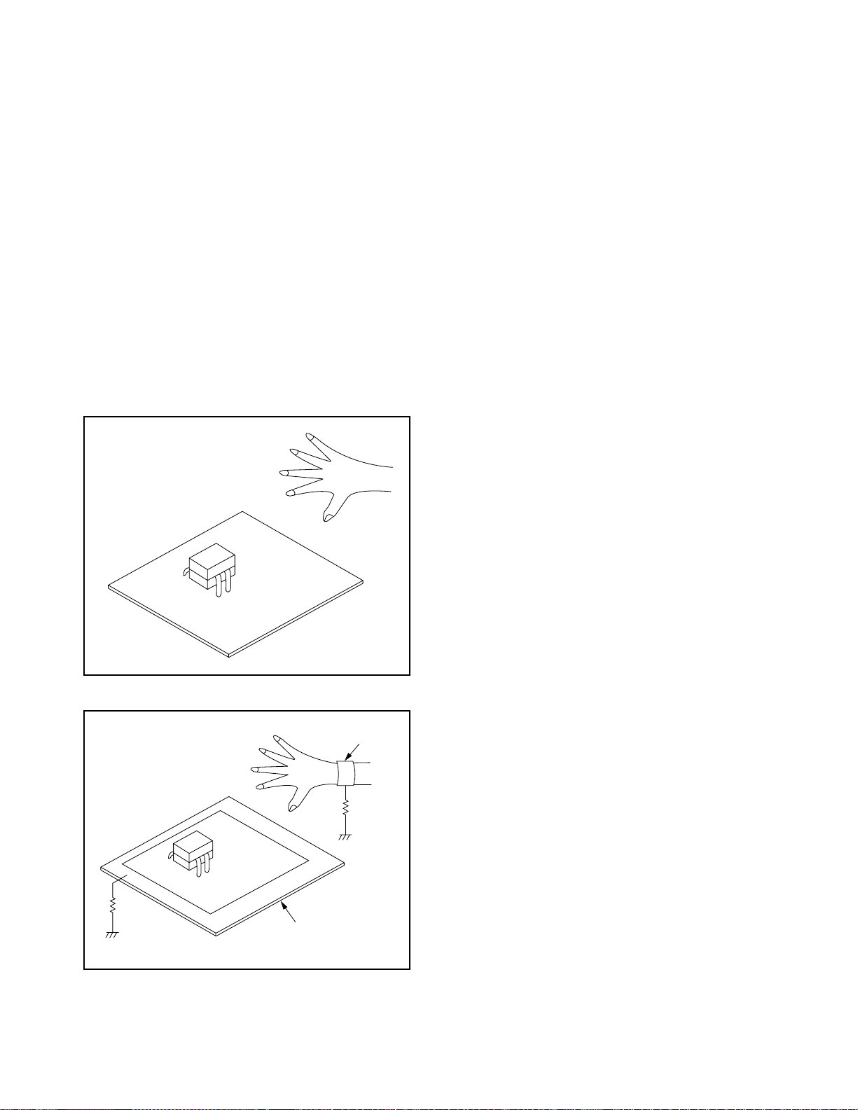
Electrostatic breakdown of the semi-conductors may
occur due to a potential difference caused by
electrostatic charge during unpacking or repair work.
1. Ground for Human Body
Be sure to wear a grounding band (1 MΩ) that is
properly grounded to remove any static electricity that
may be charged on the body.
2. Ground for Workbench
Be sure to place a conductive sheet or copper plate
with proper grounding (1 MΩ) on the workbench or
other surface, where the semi-conductors are to be
placed. Because the static electricity charge on
clothing will not escape through the body grounding
band, be careful to avoid contacting semi-conductors
with your clothing.
<Incorrect>
<Correct>
1MΩ
CBA
Grounding Band
1MΩ
CBA
Conductive Sheet or
Copper Plate
1-4-4 DVDN_SN
Page 11
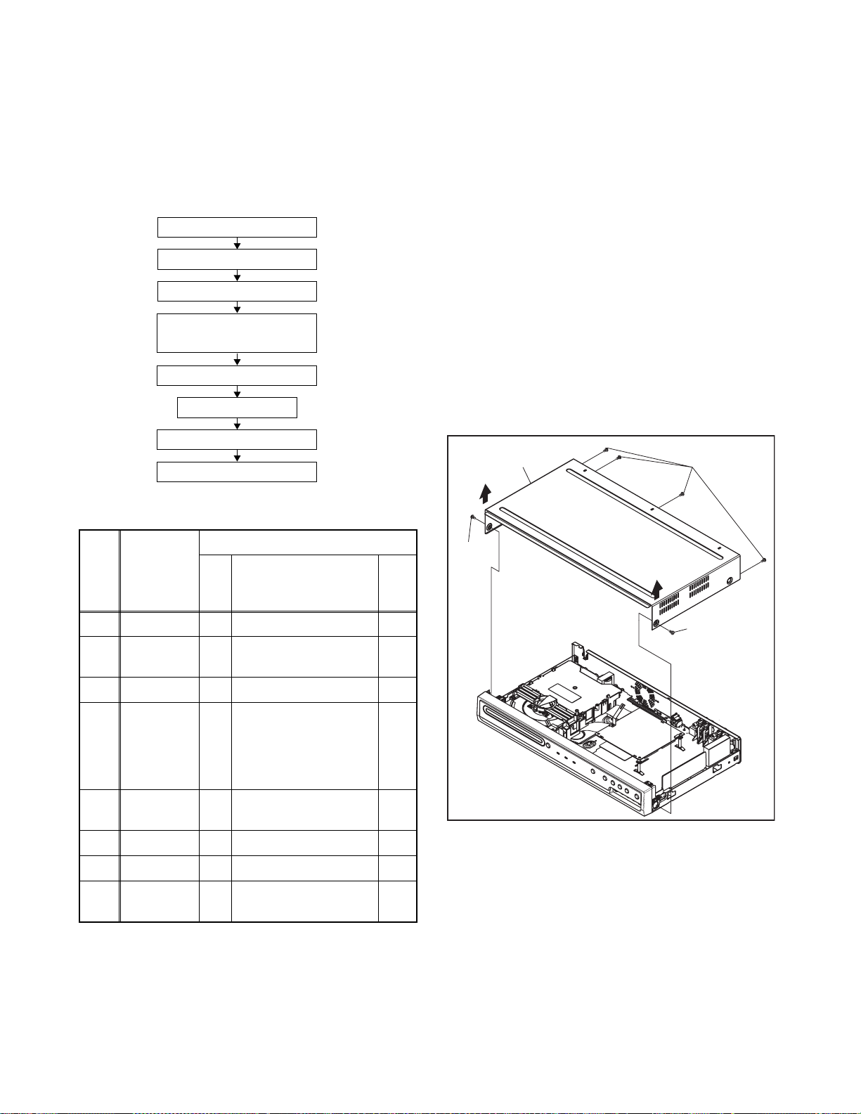
CABINET DISASSEMBLY INSTRUCTIONS
1. Disassembly F lowchart
This flowchart indicates the disassembly steps to gain
access to item(s) to be serviced. When reassembling,
follow the steps in reverse order. Bend, route, and
dress the cables as they were originally.
[1] Top Cover
[2] Front Assembly
[3] SW CBA
[4] DVD Mechanism &
DVD Main CBA Assembly
[5] Power Supply CBA
[6] Rear Panel
[7] AV CBA
[8] Front Bracket
2. Disassembly Metho d
Note:
(1) Identification (location) No. of parts in the figures
(2) Name of the part
(3) Figure Number for reference
(4) Identification of parts to be removed, unhooked,
unlocked, released, unplugged, unclampe d, o r
desoldered.
P = Spring, L = Locking Tab, S = Screw,
CN = Connector
* = Unhook, Unlock, Release, Unplug, or Desolder
e.g. 2(S-2) = two Screws (S-2),
2(L-2) = two Locking Tabs (L-2)
(5) Refer to “Reference Notes.”
Reference Notes
1. CAUTION 1: Locking Tabs (L-1) and (L-2) are
fragile. Be careful not to break them.
[1] Top Cover
(S-1)
ID/
Loc.
No.
[1] Top Cover D1 6(S-1) --[2]
[3] SW CBA D2 *2(L-3) ---
[4]
[5]
[6] Rear Panel D5 (S-5), (S-6), 6(S-7) ---
[7] AV CBA D5 5(S-8) --[8]
↓
(1)
Part
Front
Assembly
DVD
Mechanism
& DV D Main
CBA
Assembly
Power
Supply
Front
Bracket
CBA
↓
(2)
Fig.
No.
*5(L-1), *3(L-2),
D2
*CN1061
(S-2), 4(S-3), *CN101,
*CN701,
D3
PCB Support / PCB
Spacers,
M-PCB Plate Earth
D4 4(S-4), *CN1060 ---
D5 (S-9) ---
↓
(3)
Removal
Remove/*Unhook/
Unlock/Release/
Unplug/Desolder
↓
(4)
(S-1)
Note
(S-1)
1
---
Fig. D1
↓
(5)
1-5-1 E7H50DC
Page 12
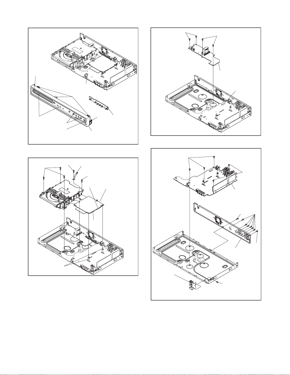
(S-4)
(S-4)
(L-1)
(L-2)
(S-3)
(L-3)
(L-2)
CN1061
(L-1)
[2] Front Assembly
(S-2)
M-PCB Plate Earth
(S-3)
CN701
(L-1)
[3] SW CBA
Fig. D2
[4] DVD
Mechanism
& DVD Main
CBA Assembly
(S-8)
[5] Power
Supply CBA
CN1060
[7] AV CBA
(S-6)
Fig. D4
(S-8)
(S-7)
PCB Support /
PCB Spacers
CN101
Fig. D3
(S-5)
[6] Rear Panel
[8] Front
Bracket
(S-9)
Fig. D5
1-5-2 E7H50DC
Page 13
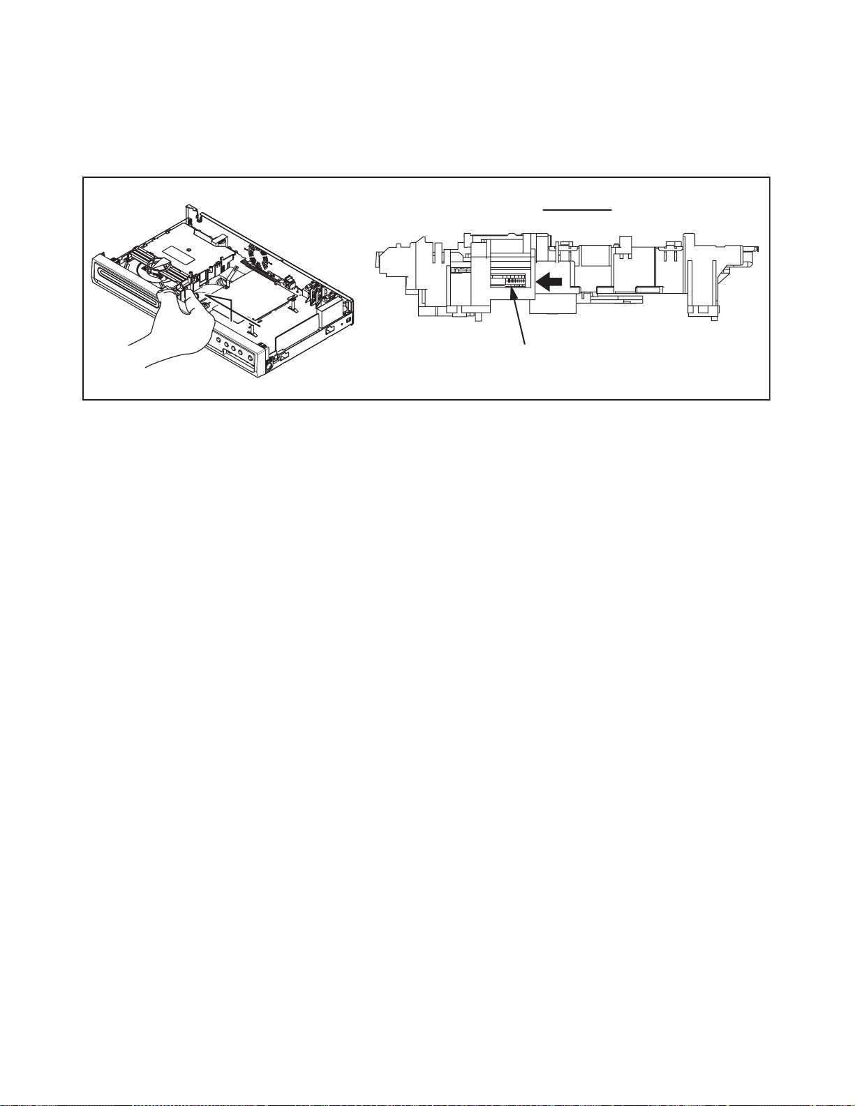
3. How to Eject Manually
Note: When rotating the gear, be careful not to damage the gear.
1. Remove the Top Cover.
2. Rotate the gear in the direction of the arrow manually as shown below until the tray descends.
3. Pull the tray out manually and remove a disc.
View for A
A
Rotate this gear in
the direction of the arrow
1-5-3 E7H50DC
Page 14

HOW TO INITIALIZE THE DVD RECORDER
To put the program back at the factory-default,
initialize the DVD recorder as the following procedure.
1. Turn the DVD recorder on.
2. Confirm that no disc is loaded or that the disc tray
is open. To put the DVD recorder into the Version
display mode, press [CM SKIP], [1], [2], and [3]
buttons on the remote control in the order.
Fig. a appears on the screen.
*1: "
*2: Firmware Version differs depending on the
models, and this indication is one example.
Fig. a Version Display Mode Screen
" differs depending on the models.
*******
F/W VERSION DISP
MODEL NAME :
DTV-S VERSION :
FE VERSION :
BE VERSION :
TT VERSION :
LD ADJUSTMENT :
DISC ADJUSTMENT :
DEFAULT SETTING : ENTER
EXIT : RETURN
*******
0x**
R40_***_***
RD4A*****S1E
T4****RDU
OK
OK
3. Press [OK] button, then the DVD recorder starts
initializing. When the initializing is completed, the
DVD recorder exits the Version display mode and
turns off the power automatically.
* To move into the Normal mode from the
V ersion display mode, press [RETURN] button
on the remote control instead of [OK] button.
* When [STANDBY-ON] button is pressed
before [OK] button is pressed, the DVD
recorder exits the Version display mode, then
the power turns off.
1-6-1 E7H50INT
Page 15
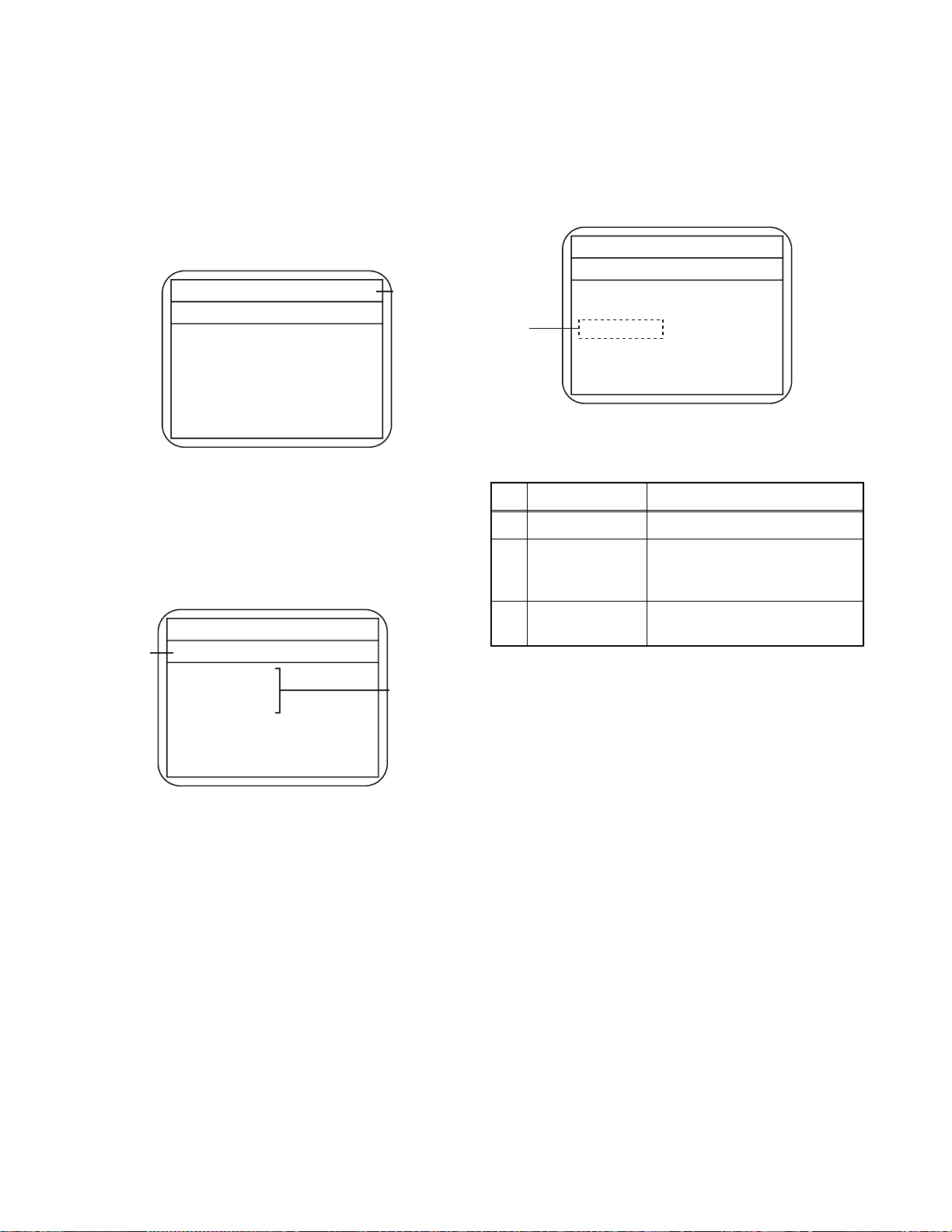
FIRMWARE RENEWAL MODE
1. Turn the power on and remove the disc on the tray.
2. To put the DVD recorder into version up mode,
press [CM SKIP], [6], [5], and [4] buttons on the
remote control unit in the order. Then the tray will
open automatically.
Fig. a appears on the screen.
* Firmware Version differs depending on the
models, and this indication is one example.
Firm Update Mode
Please insert a disc.
ver. RD4P*****H1E
Current
F/W version
is displayed.
Fig. a Version Up Mode Screen
3. Load the disc for version up.
Fig. c appears on the screen. The file on the top is
highlighted as the default.
When there is only one file to exist, Step 4 will
start automatically.
* Firmware Version differs depending on the
models, and this indication is one example.
Firm Update Mode ver. RD4P*****H1E
Disc name
is displayed.
VOL_200703250934
1 RD4P10210H1E
2 RD4P10211H1E
3 RD4P10212H1E
4 RD4P10213H1E
Files included
in the disc are
displayed.
1 / 1
4. Select the firmware version pressing arrow
buttons, then press [OK].
Fig. d appears on the screen. The DVD recorder
starts updating.
* Firmware Version differs depending on the
models, and this indication is one example.
Firm Update Mode ver. RD4P*****H1E
(*1)
File Loading...
Fig. d Programming Mode Screen
The appearance shown in (*1) of Fig. d is
described as follows.
No. Appearance State
1 File Loading... Sending files into the memory
Firmware
2
Updating...
Writing new version data
XX% Complete.
Firmware
---
Update Failure
Failed in updating
5. After updating is finished, the tray opens
automatically.
At this time, no button is available.
6. Pull out the AC code once, then insert it again.
Fig. c Update Disc Screen
1-7-1 E7H50FW
Page 16
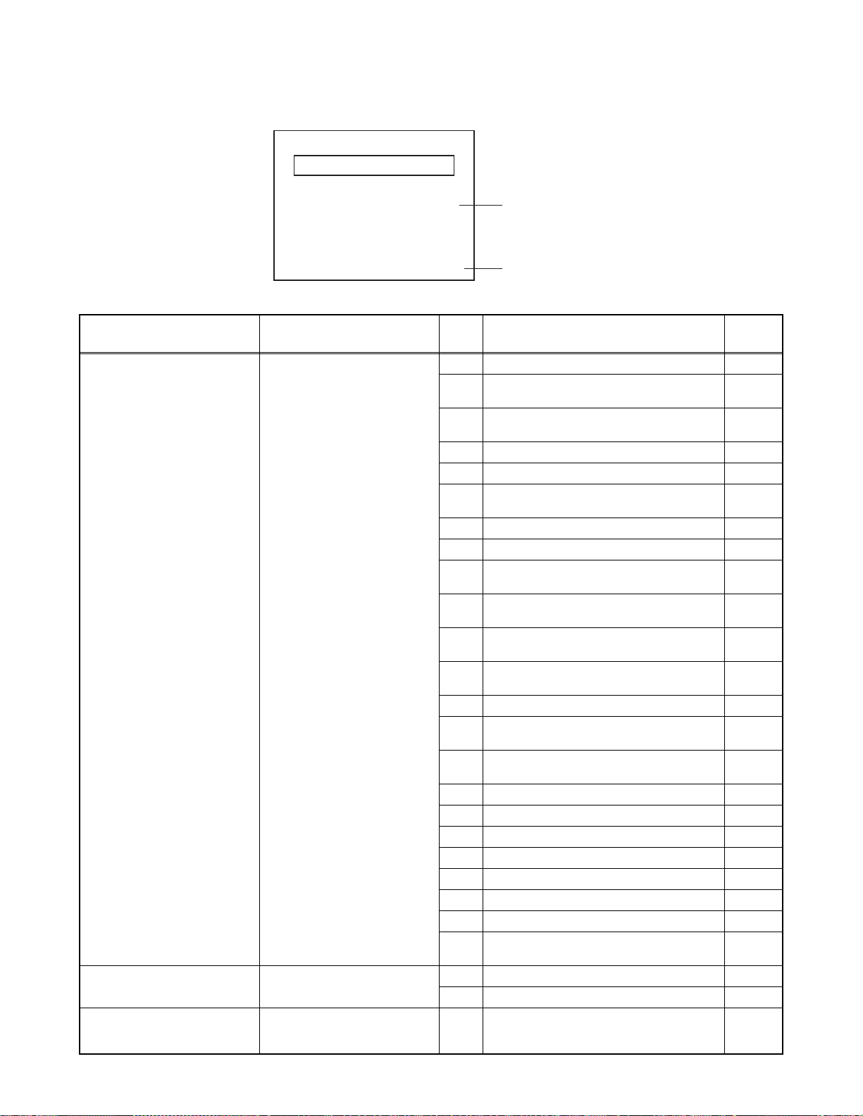
FUNCTION INDICATO R SYMBOLS
Note: If an error occurs, a message with the error number appears on the screen.
Recording Error
Message Solution
Can not record on this disc.
This program is not all o wed to
be recorded.
This disc is protected and not
recordable.
You cannot record on this disc as
Power Calibration Area is full.
Insert the recordable disc , and
ensure the disc status satisfies
the recording requirements.
You cannot record copy
prohibit ed programs.
Release the disc protect
setting in the Disc Setting
menu.
Error message
E35
Error
No.
1 An error occurs during data reading. 2
3
4 An error occurs with OPC. -
5 During recovery in a record. 6
7 An error occurs in a format. -
8 It cannot start an encode. 9
10
11
12
13 It is a reply th at “ATAPI is not readable.” 14
15
16 An error occurs in Finalize Close. -
17 An error occurs in Rec Stop Close. 18 An error occurs in PCA Full (DVD_R). 19 Safety Stop occurs during editing. 20 Hi gh Speed Disc. 2
21 The disc is not formatted. 5
22 Disc Error has occurred. 3
24
25 During the Macrovision picture input. 11
26 During the CGMS picture input. 12
29 Disc Protected Disc. 6
Error No.
Error Description Priority
There is no reply for 15 seconds in Test
Unit Ready.
Cannot write the data after trying three
times.
An error occurs e ven if re cov ery has been
tried three times.
NV_PCK/RDI_PCK is not in encoded
data.
Encode Paus e c ond iti on c ont in ue d for 10
minutes.
Encode Pause condition conti nued in
normal REC condition for 10 minutes.
Difference i n the address and can not get
StreamID of RDI/VIDEO.
Cannot write the data after recov e ring
SMALL VMGI.
Cannot write the data after D VD-R
Reverse Track.
The disc except DVD-R/RW or finalized
DVD-R.
-
-
-
-
-
-
-
-
-
1
1-8-1 E7H50FIS
Page 17
Message Solution
Disc is full.
(No area for new recording)
You cannot record on this di sc
as Power Calibration Area is
full.
This disc is already finalized.
Can not record on this disc. Repeat the same opera tio n.
You cannot record more than
49 titles on the disc.(The
maximum is 49.)
You cannot record more than
254 chapters on the disc.(The
maximum is 254.)
This program is not recordab le
in +VR mode.
The disc has a different menu
layout. (Set “Replace Disc
Menu” to ON to rewrite the
menu.)
Insert the recordable disc with
enough recording space.
Insert a new disc. 35 PCA is Full. (in REC start) 4
Release the finalizing for this
disc.
Delete unnecessary titles. 43 Its recording capacity has been reached. 9
Delete unnecessary chapter
marks.
You cannot record copy
prohibit ed programs.
Set “Replace Disc Menu” to
“ON” to rewrite the menu,after
that you will record to.
Error
No.
Error Description Priority
30 No avilable recording sp ace. 10
36 It is finalized. (Video For mat Disc) 8
37 Access to Memory Area range outside. -
38 Sector Address is wrong. 39 BUP writing error of chapter editing. -
44 The 254 chapter has been reached. 10
45 During the CGMS picture input. 12
Trying to record onto the +VR formatting
46
disc that had been recorded by the other
recorder.
7
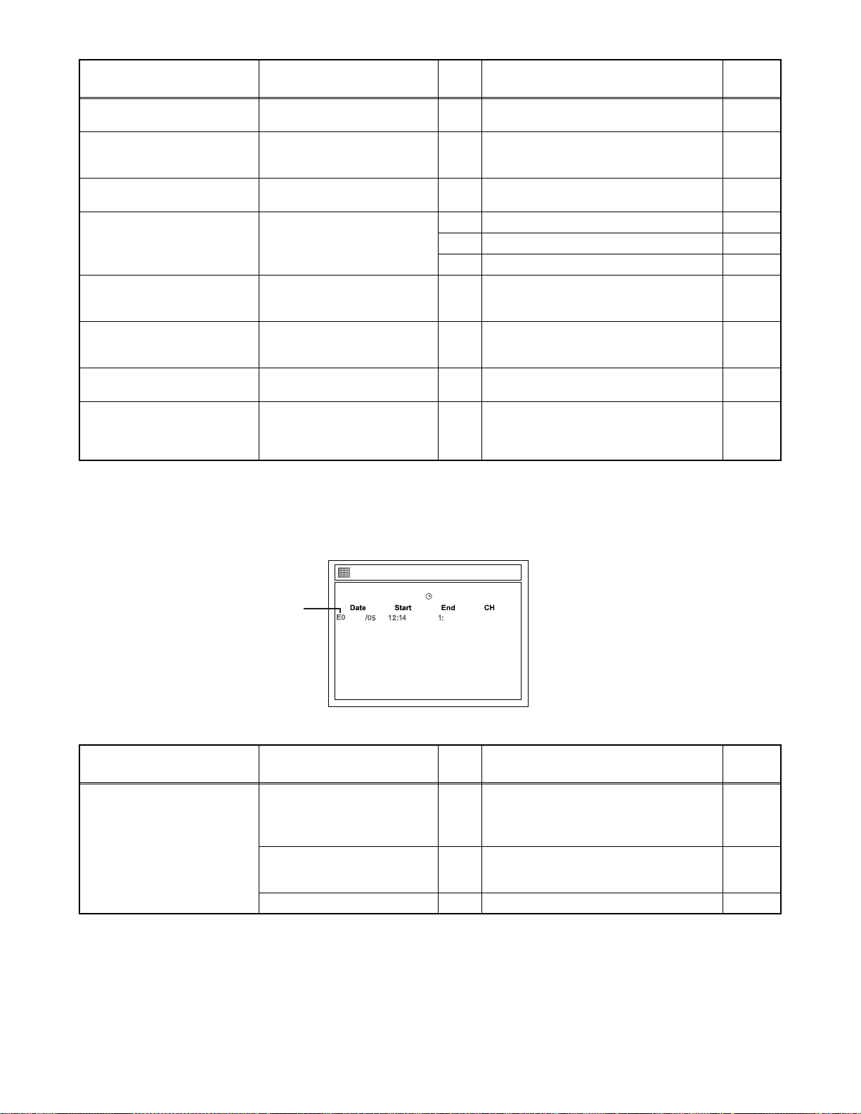
If an error occurs during the timer recording, one of the following error numbers (40 to 42) or the above error
messages (error number: 1 to 39 and 43 to 46) is displayed on the recording menu after timer recording.
(Once the screen of the program line is exited, the program line for the error will be cleared.)
(No Error Message is displayed for the error No. 40 ~ 42.)
Ti
mer Programming
JAN / 5/07 12:14AM CH4 SP
SP (1:00) FRI JAN/05 12:17AM
JAN AM 14AM
New Program
4
Error
No.
- Some portion has not been recorded
40
- Recording did not start at the start time.
41 Power failed -
Error Description Priority
because of program overlapping.
A program with an error number is grayed out and asterisked on the timer programming list.
Message Solution
Error message is not
displayed.
error number
- Set the timer programming
correctly.
- Set the timer programming
before the start time.
Turn the power on and set the
clock correctly then set timer
programming again.
Insert the record able disc. 42 No disc when recording -
-
1-8-2 E7H50FIS
Page 18
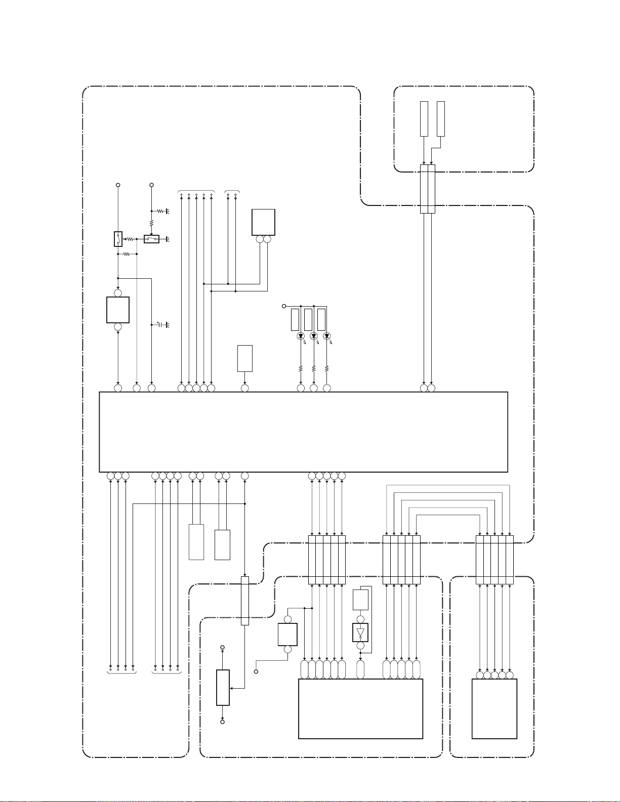
BLOCK DIAGRAMS
System Control Block Diagram
KEY SWITCH
KEY SWITCH
SW CBA
IC1501
(SUB MICRO CONTROLLER)
Q1501
IC1502
POW-SW
3
EV+3.3V
RESET
1 2
14
RESET
REG-CONT
PWSW
52
53
30
P-DOWN
EV+5V
Q1502
C1501
(BACKUP CAPACITOR)
7
VCC
VIDEO-SW1
41
42 VIDEO-SW2
AUDIO-SW1
AUDIO-MUTE
38
40
AUDIO-SW1
AUDIO-MUTE
43 VIDEO-SW3
44 VIDEO-MUTE
TO AUDI O
BLOCK DIAGRAM
SDA
AUDIO-SW2
33
39
SDA
AUDIO-SW2
X OUT
X IN
8
9
SCL
34
SCL
TO DTV MODULE
BLOCK DIAGRAM
SCL
SDA
RE2001
XC OUT
XC IN
12
11
(MEMORY)
IC1757
SENSOR
REMOTE
29
REMOTE
1V2CONT
26
33KEY-1
55KEY-2
SDA
SCL
5
6
EV+3.3V
REC
TIMER
POWER
D2001
D2002
D2003
CN1061 CN1062
AV CBA
60
59
LED1
LED2
SYS-RESET
2219182029
58
LED3
SUB-RXD
SUB-TXD
SUB-SCLK
RDY
2
KEY-1 1
KEY-2
POW-SW
REG-CONT
PWSW
TO POWER SUPPLY
BLOCK DIAGRAM
1V2CONT
VIDEO-SW2
VIDEO-SW3
VIDEO-SW1
TO VIDEO
BLOCK DIAGRAM
8MHz
X1501
VIDEO-MUTE
CN1101
RESONATOR
32.768KHz
X'TAL
X1502
DTV-S-SREQ
DTV-S-SCLK
DTV-S-SIN
DTV-S-SOUT
DTV-S-RESET
66
55
44
33
22
A4
R23
U22
R22
W25
DTV-S-SIN
DTV-S-SCLK
DTV-S-SOUT
DTV-S-SREQ
DTV-S-RESET
DVD MAIN CBA UNIT
EV+2.8VP-ON+1.2V
+1.2V
IC106
REGULATOR
111V2CONT
CN101 CN1051
IC107
P-ON+1.8V
RESET
2 1
IC101
(MAIN MICRO CONTROLLER)
27 27SYS-RESET
30 30SUB-RXD
CN701
R2
V25
R25
SUB-RXD
SYS-RESET
SYS-RESET
28 28SUB-TXD
26 26SUB-SCLK
29 29RDY
B4
P22
W26
RDY
SUB-TXD
SUB-SCLK
X501
IC501
27MHz
X'TAL
4 2
L1
CLK 27 IN
CN501 CN1753
1-9-1
IC101
(DTV SIGNAL PROCESS)
CN1751CN101
12
DTV-S-RESET
12
204
DTV-S-RESET
9
10
DTV-S-SIN
DTV-S-SOUT
9
10
154
153
DTV-S-SIN
DTV-S-SOUT
8
DTV-S-SCLK
8
155
DTV-S-SCLK
7
DTV-S-SREQ
7
38
DTV MODULE CBA UNIT
DTV-S-SREQ
E7H50BLS
Page 19
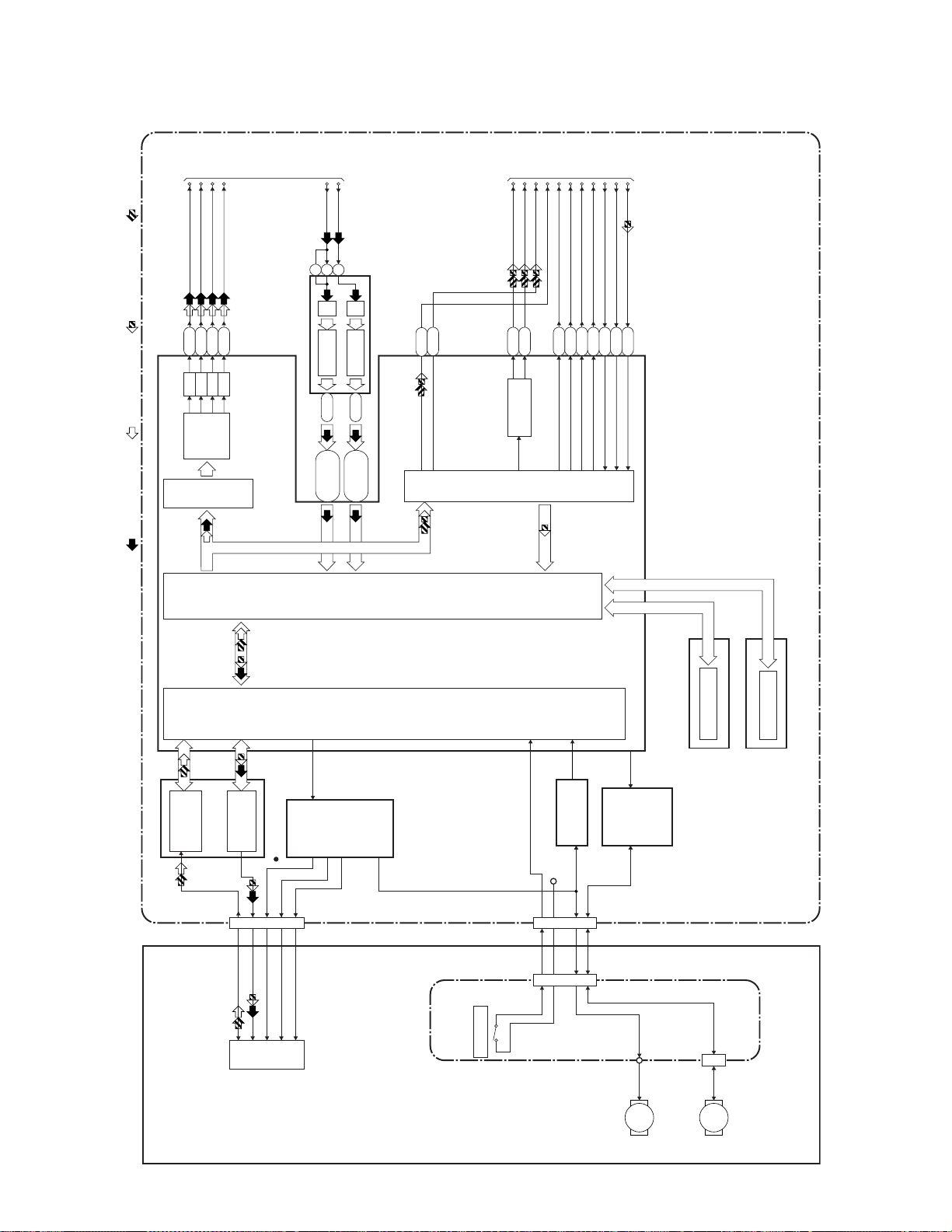
Digital Signal Process Block Diagram
TO VIDEO
BLOCK
DIAGRAM
/CVBS
VIDEO-Y(I/P)
F2
D/A
REC VIDEO SIGNAL PB VIDEO SIGNAL REC AUDIO SIGNAL PB AUDIO SIGNAL
VIDEO-C
VIDEO-Pr/Cr
VIDEO-Pb/Cb
J3
K5
D/A
D/A
VIDEO
ENCODER
VIDEO
I/F
F1
D/A
VIDEO-Y
VIDEO-C
10813
A/D
DECODER A/D
DECODER
IC701 (VIDEO DECODER)
45-50
39-44
U2,U3,V1
P3,T3,T5,
U4,W1,W3,
Y2,AA1,AA2
P1
R4
TO AUDI O
SPDIF
AUDIO (L)-OUT
AUDIO (R)-OUT
DVD-AUDIO-MUTE
D1
D3
AUDIO D/A
CONVERTER
AUDIO
I/F
BLOCK
AIMS
E12
DIAGRAM
MD
Y26
MC
U24
LRCK
SYSCLK
K2
M3
BCK
DATA
K1
N4
DVD MAIN CBA UNIT
(MAIN MICRO CONTROLLER)
IC101
IC201
RF/
ERROR AMP
CN201
LPC
LPC
TILT
PICK
IC301
TRACKING
-UP
FOCUS
MOTOR
DRIVER
BACK-END
DIGITAL
SIGNAL
FRONT-END
DIGITAL
SIGNAL
PROCESS
PROCESS
TRAY OPEN
CN301
CN1001
IC202
+3.3V
OP AMP
IC302
MOTOR
DRIVER
IC104 (FLASH MEMORY)
FLASH MEMORY
CN1002
DDR SDRAM
IC102 (DDR SDRAM)
RELAY CBA
DVD MECHANISM
1-9-2
SLED
MOTOR
M
SPINDLE
MOTOR
M
E7H50BLD
Page 20
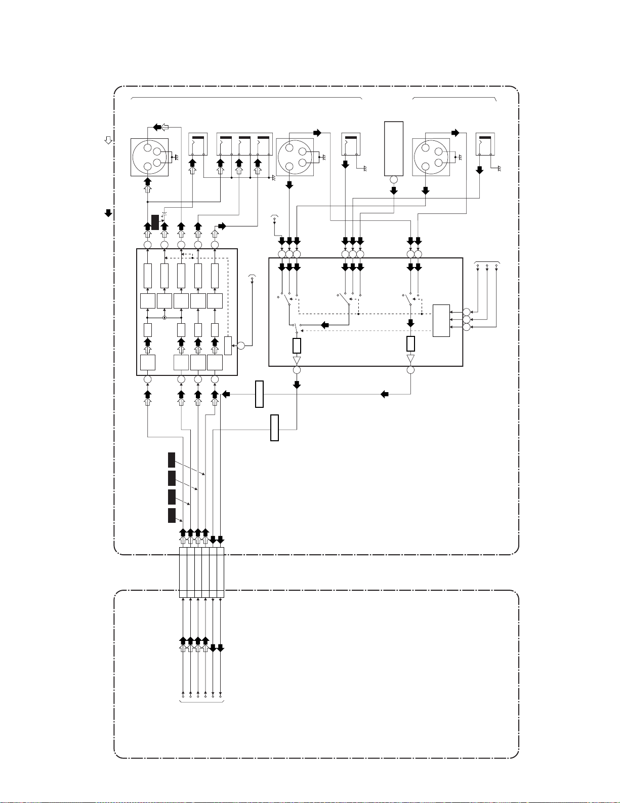
Video Block Diagram
JK2202
S-VIDEO
OUT
C
3 4
Y
REC VIDEO SIGNAL PB VIDEO SIGNAL
13
2dB
LPF DRIVER
4dB
IC1401 (VIDEO DRIVER)
3
AMP
AMP
2
1
WF3
14
DRIVER
8dB
AMP
-6dB
C1418
2dB
4dB
JK2201
15
AMP
LPF DRIVER
AMP
1
VIDEO-OUT
JK2203
11
10
DRIVER
2dB
AMP
2dB
LPF DRIVER
LPF
4dB
AMP
4dB
6
8
VIDEO-Y
AMP
AMP
OUT
MUTE
REAR
VIDEO
-Pb/Cb OUT
VIDEO
-Pr/Cr OUT
TO DTV
TO SYSTEM
CONTROL
BLOCK DIAGRAM
VIDEO-MUTE
5
IC1301
(VIDEO INPUT SELECT)
MODULE
BLOCK
DIAGRAM
DTV-V
17
D-V
MUTE
JK2105
S-VIDEO
C
3 4
Y
13
Y2
Y1
15
LPF
19
IN1
FRONT
JK2101
S-VIDEO
221
LPF
IN2
C
2
1
3 4
Y
4
CONTROL
LOGIC
JK2102
VIDEO-SW1
24
22 23
VIDEO
-IN2
TO SYSTEM CONTROL
BLOCK DIAGRAM
VIDEO-SW2
VIDEO-SW3
VIDEO-IN1
2
1
JK2106
MUTE
8
10
VIDEO2
VIDEO1
TU1701 (TUNER UNIT)
12
TUNER
VIDEO OUT
4
MUTEC2C1
WF5
WF4
WF1 WF2
CN1101
VIDEO-Y(I/P)-OUT
VIDEO-C-OUT
VIDEO-Pb/Cb-OUT
VIDEO-Pr/Cr-OUT
VIDEO-Y/CVBS-IN
77
99
33
55
20 20
22 22VIDEO-C-IN
CN701
VIDEO-Y(I/P)
VIDEO-C
VIDEO-Pb/Cb
VIDEO-Pr/Cr
VIDEO-Y/CVBS
VIDEO-C
BUFFER
Q1303
BUFFER
Q1304
AV CBA
DVD MAIN CBA UNIT
TO DIGITAL
SIGNAL
PROCESS
BLOCK
DIAGRAM
1-9-3
E7H50BLV
Page 21
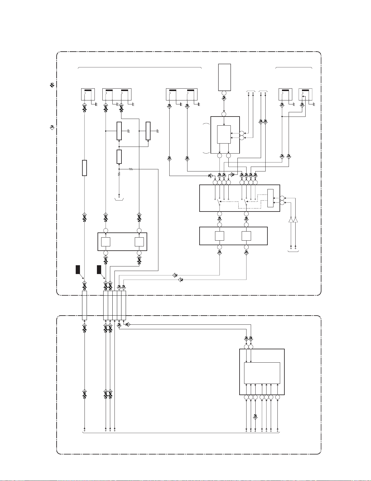
Audio Block Diagram
REC AUDIO SIGNAL PB AUDIO SIGNAL
DIGITAL
JK2206
BUFFER
Q1241
AUDIO OUT
(COAXIAL)
)
OP AMP
(
IC1201
JK2201
1
OP
2
AUDIO(L)
-OUT1
AMP
MUTE-ONDRIVE
Q1203 Q1201
AUDIO-MUTE
TO
SYSTEM
CONTROL
AUDIO(R)
-OUT1
BLOCK
VDIAGRAM
REAR
7
OP
6
AMP
MUTE-ON
Q1202
JK2106
AUDIO(L)
-IN1
AUDIO(R)
-IN1
IC1701
MTS/SAP AUDIO
(AUDIO INPUT SELECT)
IC1101
)
OP AMP
(
IC1102
(TUNER UNIT)
TU1701
SIGNAL PROCESS
111514
IN1TUIN2
(L-CH)
SIF
3
21
MTS/SAP
AUDIO
L-CH
30
13
6
OP
AMP
7
SIGNAL
PROCESS
R-CH
29
12
(R-CH)
TO SYSTEM CONTROL
SCL
24 27
425
IN1TUIN2
3
2
OP
AMP
1
BLOCK DIAGRAM
SDA
1
TO DTV MODULE
BLOCK DIAGRAM
DTV-AUDIO(L)
DTV-AUDIO(R)
SW CTL
JK2103
9 10
AUDIO(L)
-IN2
Q1102
AUDIO-SW2
FRONT
AUDIO(R)
JK2104
Q1101
AUDIO-SW1
-IN2
AV CBADVD MAIN CBA UNIT
WF7
CN1051
CN101
33SPDIF
SPDIF
WF6
AUDIO(L)-OUT
17 17
CN701 CN1101
AUDIO (L)-OUT
AUDIO (R)-OUT
AUDIO(R)-OUT
DVD-AUDIO-MUTE
AUDIO(L)-IN
AUDIO(R)-IN
15 15
18 18
11 11
13 13
DVD-AUDIO-MUTE
IC802 (AUDIO A/D CONVERTER)
13
L-CH
789
LRCK
14
R-CH
BCK
DATA
AUDIO A/D
CONVERTER
101112
MC
MD
AIMS
6
SYSCLK
TO SYSTEM CONTROL
BLOCK DIAGRAM
TO DIGITAL
SIGNAL
1-9-4
PROCESS
BLOCK
DIAGRAM
E7H50BLA
Page 22
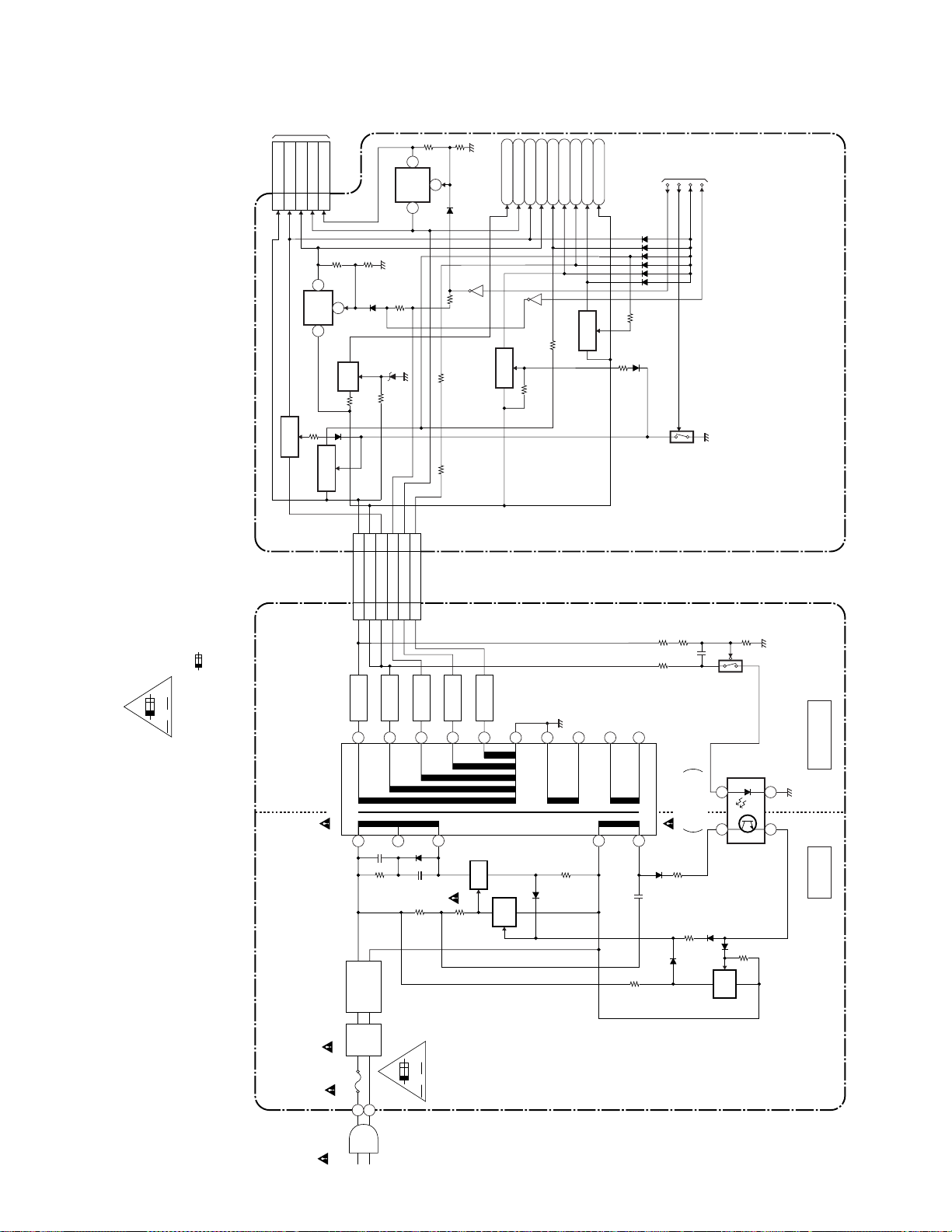
Power Supply Block Diagram
TO DVD MAIN
CBA UNIT
EV+2.8V
P-ON+1.8V
6,7
10-12
REG.
+3.3V
1 2
CN101
4
EV+10.5V
25-27
CN1051
P-ON+5V
P-ON+3.3V
20-22
15-17
IC1503
IC1504
+1.8V
1 2
REG.
TO
SYSTEM
CONTROL
BLOCK
PWSW
POW-SW
REG-CONT
DIAGRAM
1V2CONT
4
Q1505
EV+3.3V
EV+2.8V
P-ON+3.3V
P-ON+5V
Q1506
AUDIO+10V
TUNER+32V
TUNER+5V
Q1057
VIDEO+5V
EV+5V
SW+5V
NOTE:
The voltage for parts in hot circuit is measured using
hot GND as a common terminal.
SW+5V
Q1053
SW+10.5V
Q1054
"Ce symbole reprèsente un fusible à fusion rapide."
"This symbol means fast operating fuse."
CAUTION !
For continued protection against fire hazard,
Risk of fire-replace fuse as marked.
replace only with the same type fuse.
ATTENTION : Pour une protection continue les risqes
d'Incele n'utiliser que des fusible de même type.
F
A V
+3.3V
Q1063
D1063
T1001
REG.
CN1060CN1070
1-3 EV+10.5V 1-3
RECTIFIER
20
3
19,20
10-12
+5V-L
EV+4V
6-9 EV+5V 6-9
19,20
10-12
RECTIFIER
D1057, D1058
19
4
22-27
EV+2.8V
21 TUNER+32V 21
22-27
RECTIFIER
D1055
18
RECTIFIER
D1056, D1077
D1068
171516
5
SW+5V
Q1065
RECTIFIER
Q1056
Q1060
14
13
12
117
COLD
2
IC1001
ERROR
VOLTAGE DET
8
4 1
3
BRIDGE
RECTIFIER
D1001-D1004
LINE
FILTER
L1001
F
F1001
HOT CIRCUIT. BE CAREFUL.
CAUTION !
Fixed voltage (or Auto voltage selectable) power supply circuit is used in this unit.
If Main Fuse (F1001) is blown , check to see that all components in the power supply
circuit are not defective before you connect the AC plug to the AC power supply.
Otherwise it may cause some components in the power supply circuit to fail.
1A 250V
AC1001
AC CORD
A V
1-9-5
Q1002
SW
Q1001
SW
CTL
Q1003
SW
HOT
CTL
POWER SUPPLY CBA AV CBA
E7H50BLP
Page 23
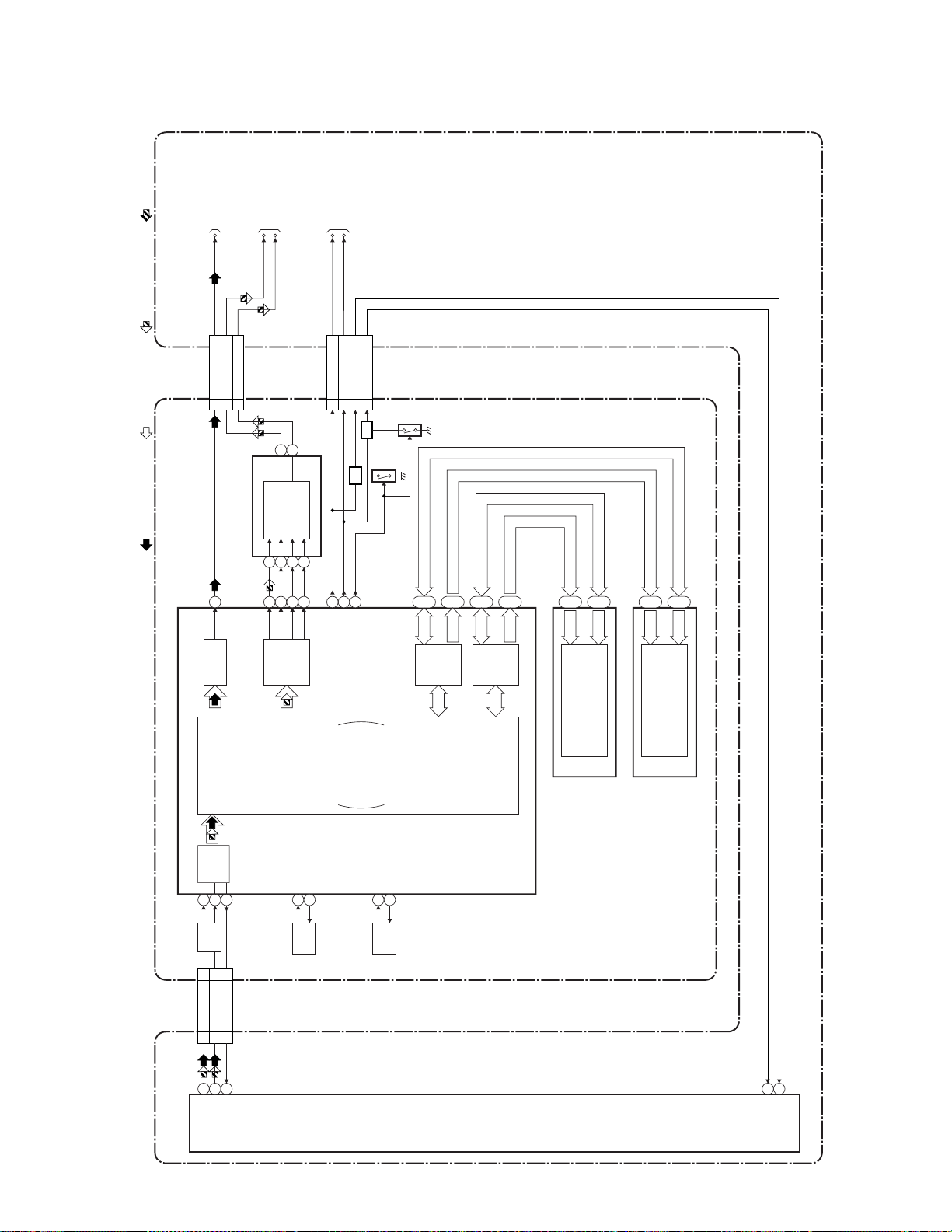
DTV Module Block Diagram
TO VIDEO
BLOCK DIAGRAM
TO AUDIO
BLOCK DIAGRAM
DTV-V
DTV-AUDIO(L)
DTV-AUDIO(R)
TO SYSTEM CONTROL
BLOCK DIAGRAM
SCL
SDA
CN1752
CN102
REC VIDEO SIGNAL PB VIDEO SIGNAL REC AUDIO SIGNAL PB AUDIO SIGNAL
DTV-AUDIO(L)
14 14DTV-VIDEO
15 15
VIDEO
ENCODER
DTV-AUDIO(R)
16 16
IC252
(AUDIO D/A CONVERTER)
6
159
L-CH
AUDIO
5 15147
158
D/A
AUDIO
R-CH
CONVERTER
8
162
161
DECODER
CN1751CN101
14 14SDA
144
SDA
15 15SCL
Q212
143
SCL
55TU-SDA
44TU-SCL
SW
Q211
SW
41
BUS-CONT
Q214
Q213
DATA BUS(0-15)
ADDRESS BUS(0-12)
*1
*2
SDRAM
I/F
DATA BUS(0-15)
ADDRESS BUS(1-22)
*3
*4
FLASH
MEMORY
I/F
*5
*6
*7
*8
AV CBA
FLASH MEMORY
IC202 (FLASH MEMORY)
DDR SDRAM
IC201 (DDR SDRAM)
IC101 (DTV SIGNAL PROCESS)
CN1752 CN102
TU1701
(TUNER UNIT)
ADC
/AGC I/F
174
178 189
140
LPF
DIF-OUT1
DIF-OUT2
DIF-AGC
99
11 11
12 12
212018
DIF AGC
DIF-OUT1
DIF-OUT2
X271
DIGITAL SIGNAL
PROCESS
27MHz OSC
27MHz OSC
14
15
27MHz
OSC
SYSTEM DECODER
/VIDEO DECODER
/VIDEO FORMAT
CONVERTER
/2D GRAPHICS
27MHz OSC
27MHz OSC
4
5
27MHz
OSC
X281
1-9-6
*1 79~81,85,87,89~91,92,94,96~98,
102,104,106
*2 55,56,58,60,61,116,119,120,124,
125,127,129,130
*3 1,2,7~12,20,206,209,211,213~216,
*4 23~25,27,29,32~36,41~44,47,48,50,
52~54,205
*5 1~10,13,16~25,48
*6 29~36,38~45
*7 28~32,35~42
*8 2,4,5,7,8,10,11,13,54,56,57,59,60,
62,63,65
DTV MODULE CBA UNIT
14
15
SCL
SDA
E7H50BLDTV
Page 24

SCHEMATIC DIAGRAMS / CBA’S
Standard Notes
WARNING
Many electrical and mechanical parts in this chassis
have special characteristics. These characteristics
often pass unnoticed and the protection afforded by
them cannot necessarily be obtained by using
replacement components rated for higher voltage,
wattage, etc. Replacement parts that have these
special safety characteristics are identified in this
manual and its supplements; electrical components
having such features are identified by the mark “#” in
the schematic diagram and the parts list. Before
replacing any of these components, read the parts list
in this manual carefully. The use of substitute
replacement parts that do not have the same safety
characteristics as specified in the parts list may create
shock, fire, or other hazards.
Notes:
1. Do not use the part number show n on these
drawings for ordering. The correct part number is
shown in the parts list, and may be slightly
different or amended since these drawings were
prepared.
2. All resistance values are indicated in ohms
(K = 10
3. Resistor wattages are 1/4W or 1/6W unless
otherwise specified.
4. All capacitance values are indicated in µF
(P = 10
5. All voltages are DC voltages unless otherwise
specified.
3
, M = 106).
-6
µF).
1-10-1 RL4N_SC
Page 25
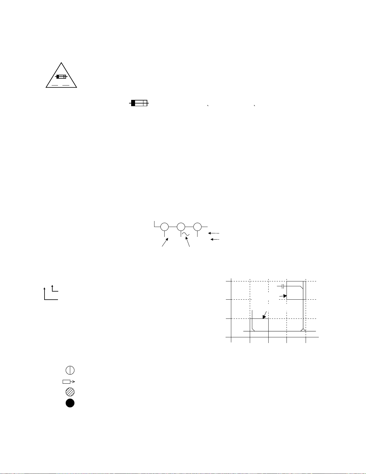
LIST OF CAUTION, NOTES, AND SYMBOLS USED IN THE SCHEMATIC DIAGRAMS ON
THE FOLLOWING PAGES:
1. CA UTION:
FOR CONTINUED PROTECTION AGA INST FIRE HAZARD, REPLACE ONLY WITH THE
F
A V
SAME TYPE FUSE.
ATTENTION: POUR UNE PROTECTION CONTINUE LES RISQES D'INCELE N'UTILISER
QUE DES FUSIBLE DE MÊME TYPE.
RISK OF FIRE-REPLACE FUSE AS MARKED.
This symbol means fast operating fuse.
Ce symbole represente un fusible a fusion rapide.
2. CA UTION:
Fixed Voltage (or Auto voltage selectable) power supply circuit is used in this unit.
If Main Fuse (F1001) is blown, first check to see that all components in the power supply circuit are not
defective before you connect the AC plug to the AC power supply. Otherwise it may cause some components
in the power supply circuit to fail.
3. Note:
1. Do not use the part number shown on the drawings for ordering. The correct part number is shown in the
parts list, and may be slightly different or amended since the drawings were prepared.
2. To maintain original function and reliability of repaired units, use only original replacement parts which are
listed with their part numbers in the parts list section of the service manual.
4. Voltag e indications for PLAY and REC mode on the schematics are as shown below:
2
1
(Unit: Volt)
The same voltage for
both PLAY & REC modes
5.0
3
5.0
(2.5)
Indicates that the voltage
is not consistent here.
PLAY mode
REC mode
5. How to read converged lines
1-D3
Distinction Area
Line Number
(1 to 3 digits)
3
1-B1
AREA D3
2
AREA B1
Examples:
1. "1-D3" means that line number "1" goes to the line number
"1" of the area "D3".
1
1-D3
2. "1-B1" means that line number "1" goes to the line number
"1" of the area "B1".
ABCD
6. Test Point Information
: Indicates a test point with a jumper wire across a hole in the PCB.
: Used to indicate a test point with a component lead on foil side.
: Used to indicate a test point with no test pin.
: Used to indicate a test point with a test pin.
1-10-2 RL4N_SC
Page 26
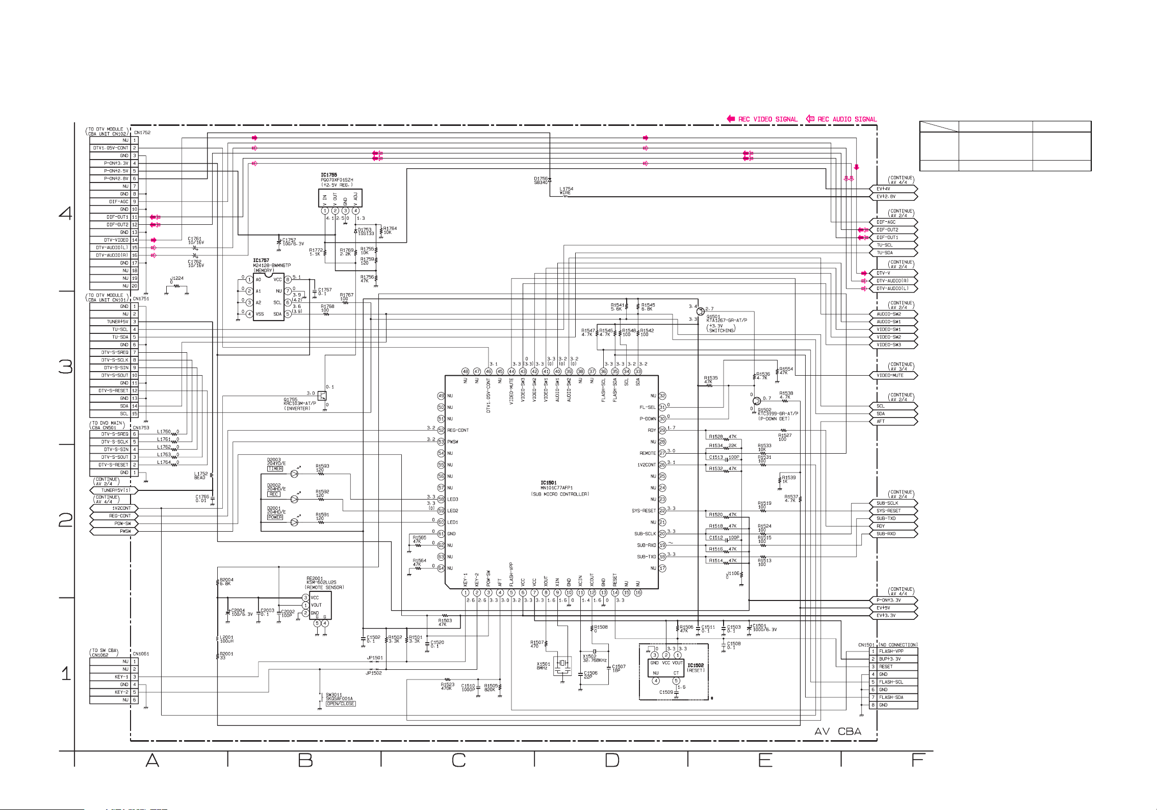
AV 1/4 Schematic Diagram
* NOTE
IC1502
R3112N191A-TR-FA
/R3112N191A-TR-FB
/BU4219G-TR
PST3619NR
Group A Group B
C1509 0.015 0.1
These components (IC1502, C1509)
can be used in any models.
However, you cannot mix components under
Group A with the ones under Group B.
You can choose either Group. The difference
between Group A and Group B is shown below.
1-10-3
E7H50SCAV1
Page 27
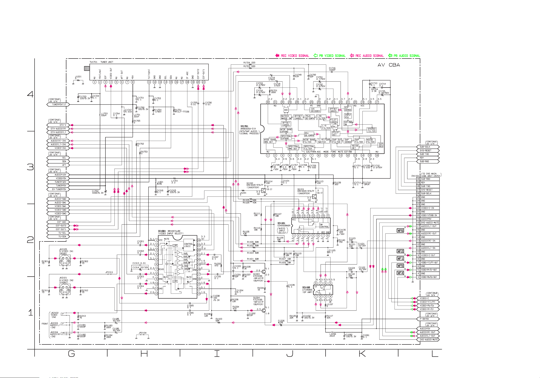
AV 2/4 Schematic Diagram
1-10-4
E7H50SCAV2
Page 28
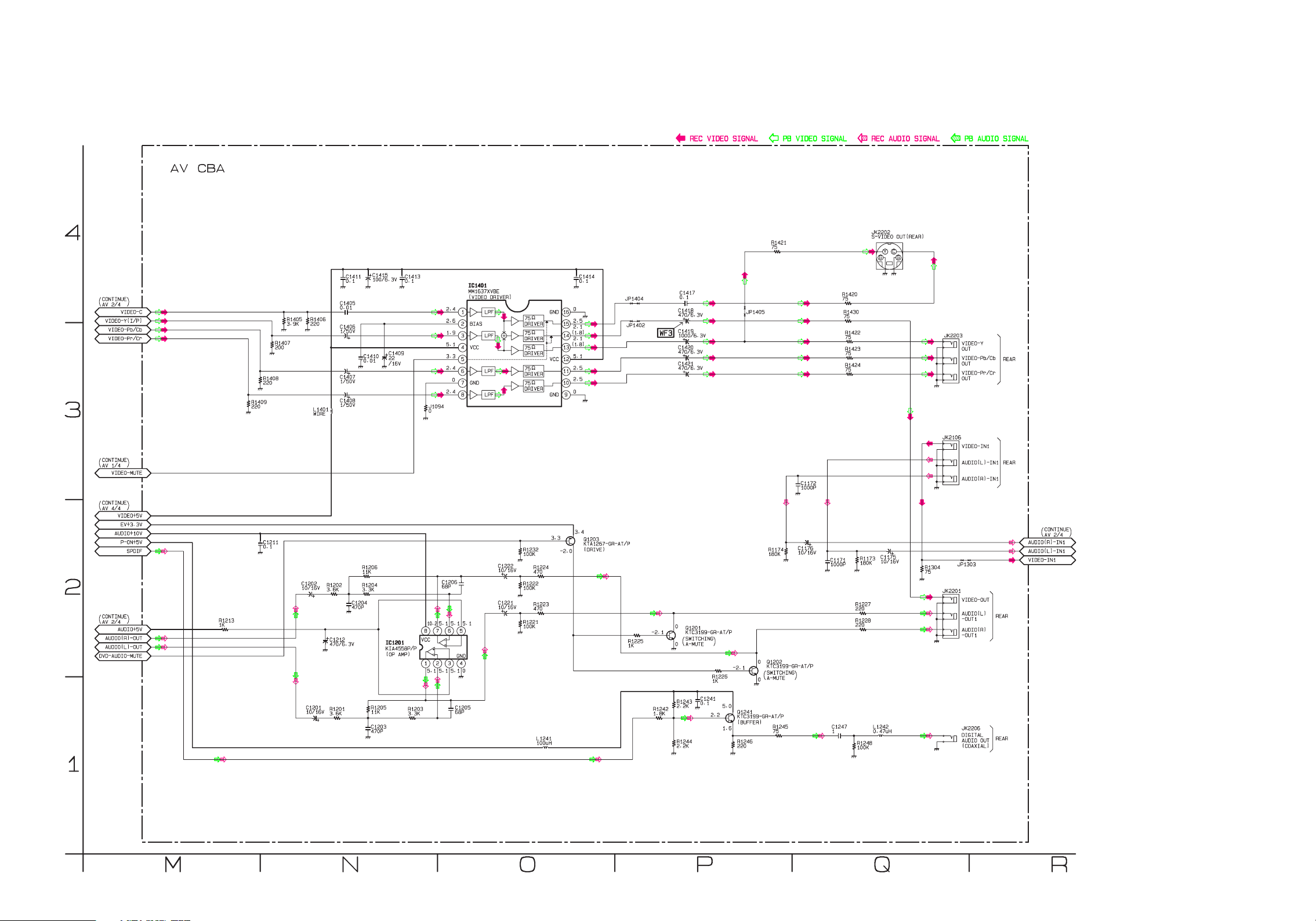
AV 3/4 Schematic Diagram
1-10-5
E7H50SCAV3
Page 29
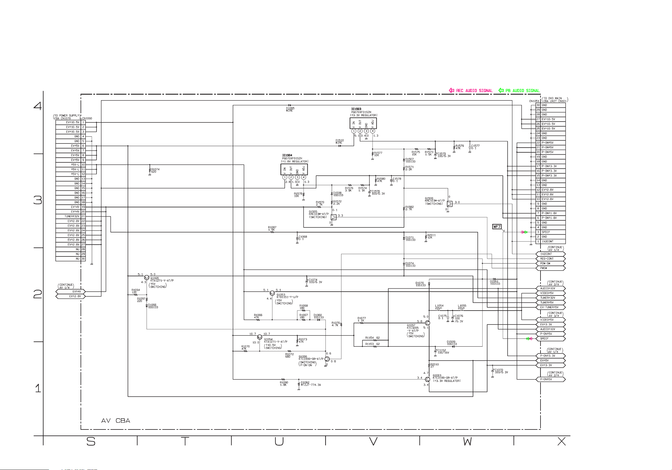
AV 4/4 Schematic Diagram
1-10-6
E7H50SCAV4
Page 30
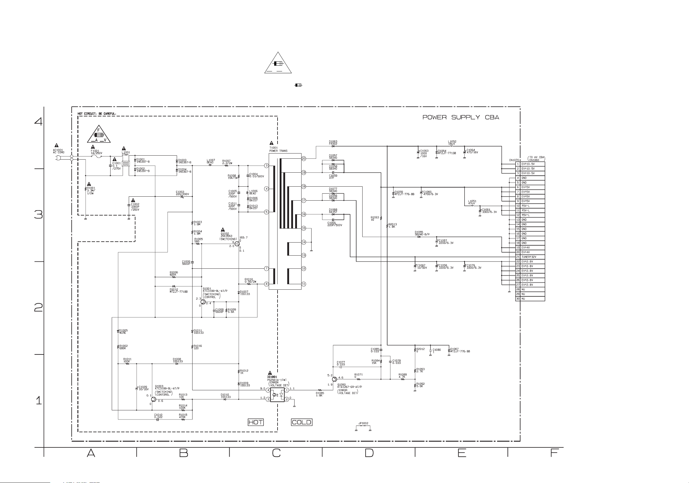
NOTE:
The voltage for parts in hot circuit is measured using
hot GND as a common terminal.
Power Supply Schematic Diagram
CAUTION !
Fixed voltage (or Auto voltage selectable) power supply circuit is used in this unit.
If Main Fuse (F1001) is blown , check to see that all components in the power supply
circuit are not defective before you connect the AC plug to the AC power supply.
Otherwise it may cause some components in the power supply circuit to fail.
F
A V
CAUTION !
For continued protection against fire hazard,
replace only with the same type fuse.
ATTENTION : Pour une protection continue les risqes
d'Incele n'utiliser que des fusible de même type.
Risk of fire-replace fuse as marked.
"This symbol means fast operating fuse."
"Ce symbole reprèsente un fusible à fusion rapide."
1-10-7
E7H50SCP
Page 31
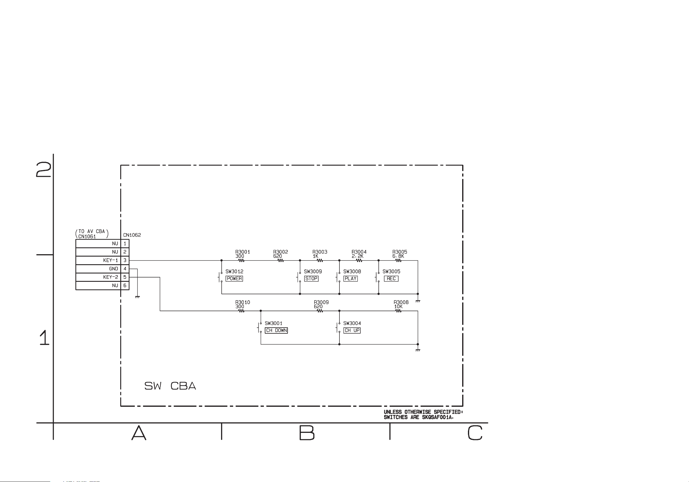
SW Schematic Diagram
1-10-8
E7H50SCSW
Page 32
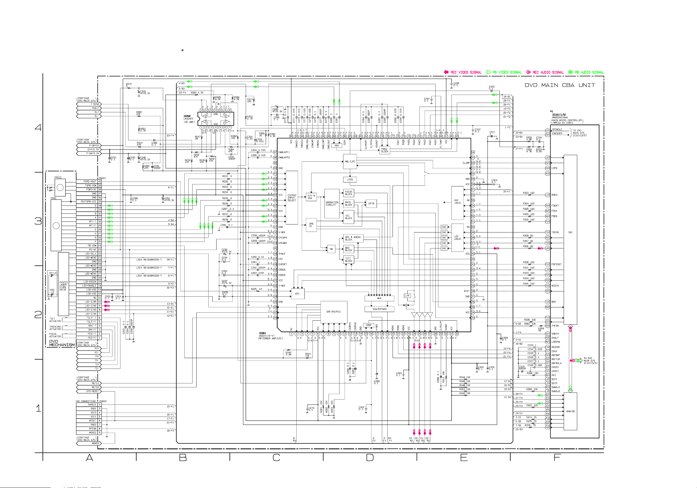
DVD Main 1/5 Schematic Diagram
1 NOTE:
The order of pins shown in this diagram is different from that of actual IC101.
IC101 is divided into five and shown as IC101 (1/5) ~ IC101 (5/5) in this DVD Main Schematic Diagram Section.
1-10-9
E7H50SCD1
Page 33
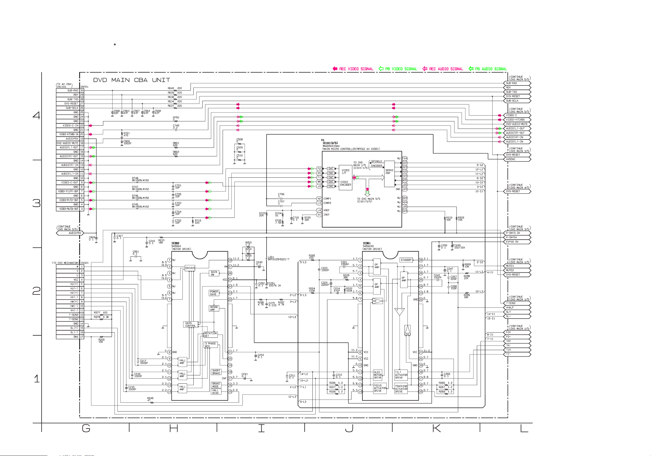
DVD Main 2/5 Schematic Diagram
1 NOTE:
The order of pins shown in this diagram is different from that of actual IC101.
IC101 is divided into five and shown as IC101 (1/5) ~ IC101 (5/5) in this DVD Main Schematic Diagram Section.
1-10-10
E7H50SCD2
Page 34
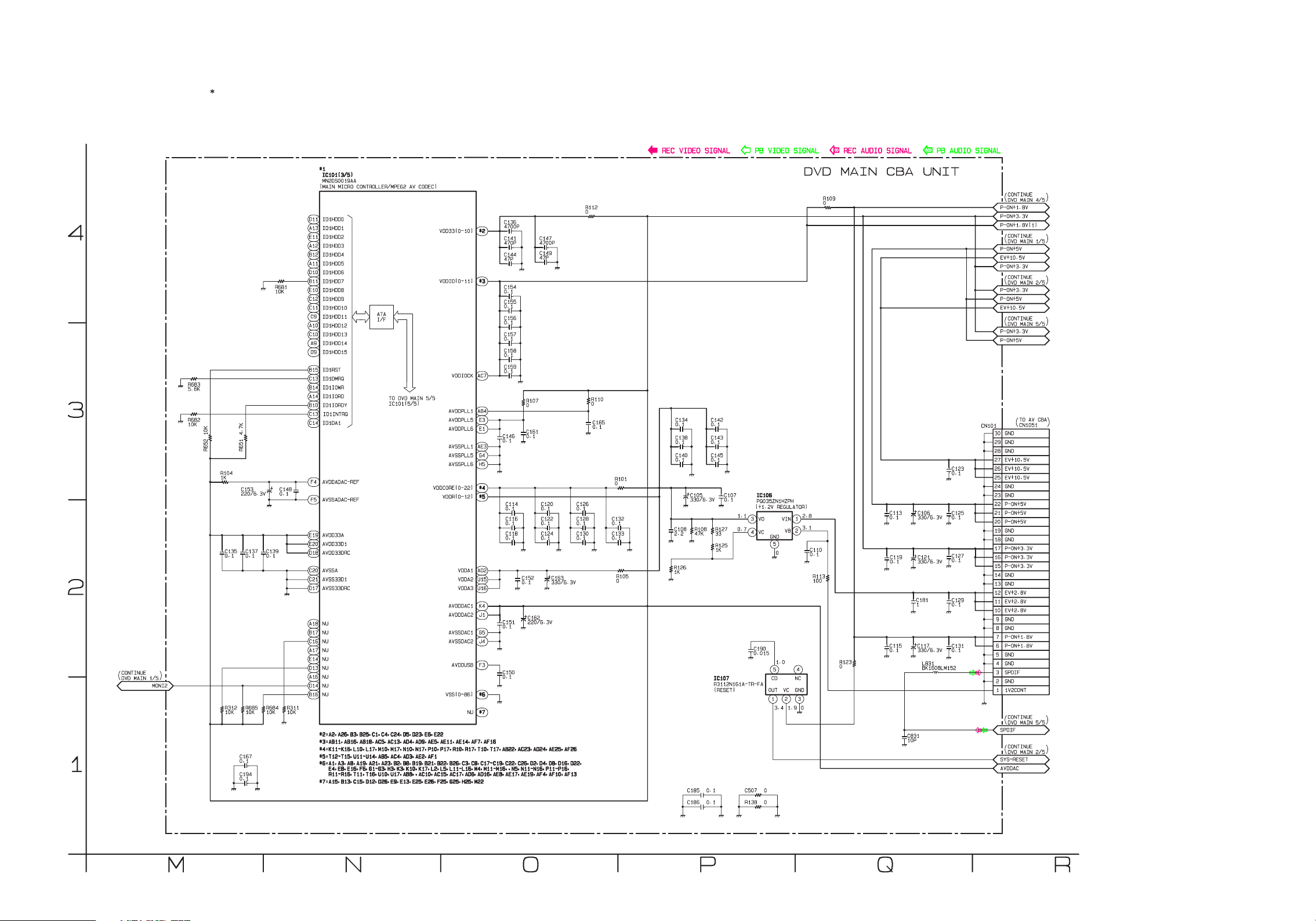
DVD Main 3/5 Schematic Diagram
1 NOTE:
The order of pins shown in this diagram is different from that of actual IC101.
IC101 is divided into five and shown as IC101 (1/5) ~ IC101 (5/5) in this DVD Main Schematic Diagram Section.
1-10-11
E7H50SCD3
Page 35
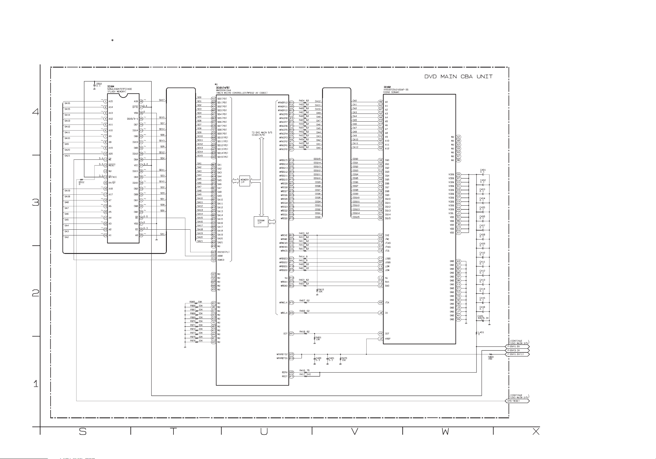
DVD Main 4/5 Schematic Diagram
1 NOTE:
The order of pins shown in this diagram is different from that of actual IC101.
IC101 is divided into five and shown as IC101 (1/5) ~ IC101 (5/5) in this DVD Main Schematic Diagram Section.
1-10-12
E7H50SCD4
Page 36
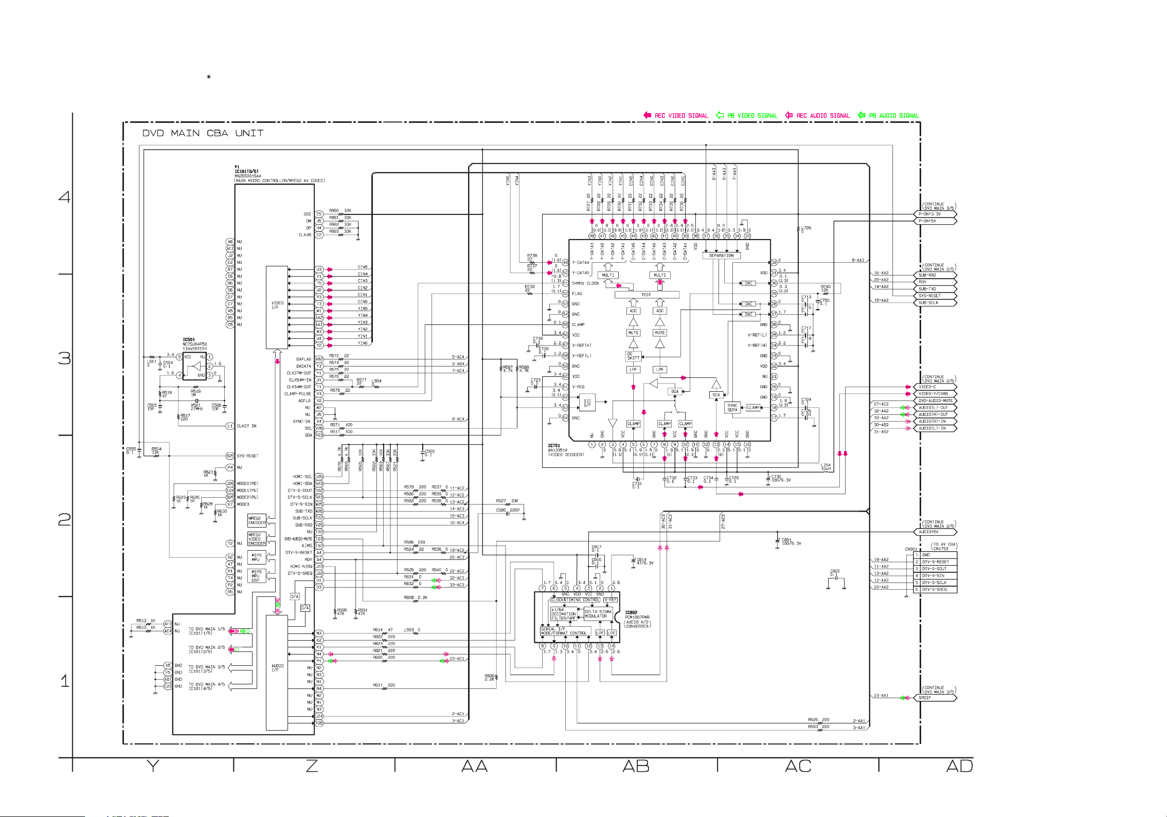
DVD Main 5/5 Schematic Diagram
1 NOTE:
The order of pins shown in this diagram is different from that of actual IC101.
IC101 is divided into five and shown as IC101 (1/5) ~ IC101 (5/5) in this DVD Main Schematic Diagram Section.
1-10-13
E7H50SCD5
Page 37
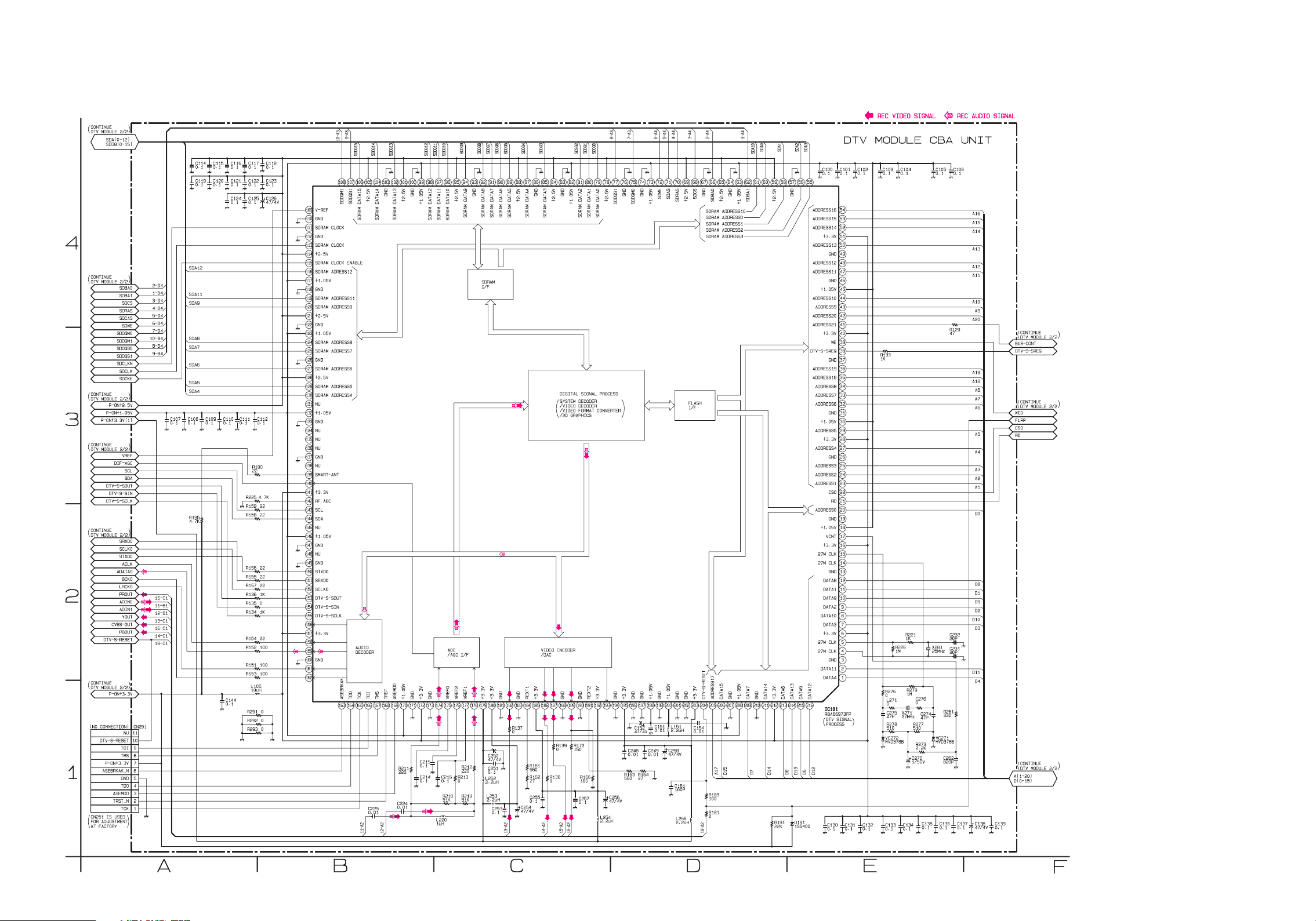
DTV Module 1/2 Schematic Diagram
1-10-14
E7H50SCDTV1
Page 38
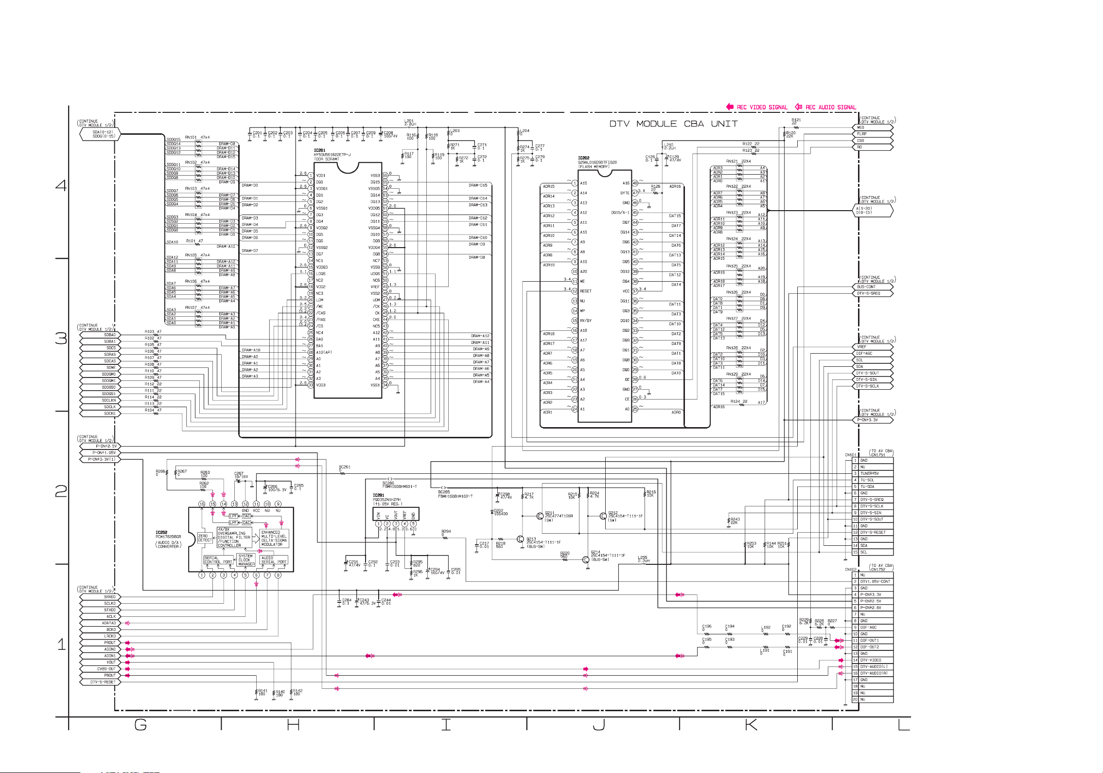
DTV Module 2/2 Schematic Diagram
1-10-15
E7H50SCDTV2
Page 39
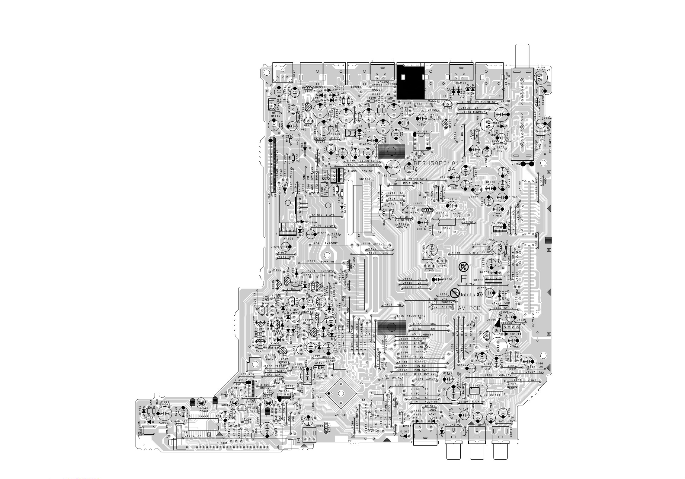
AV CBA Top View
1-10-16
BE7H50F01013A
Page 40
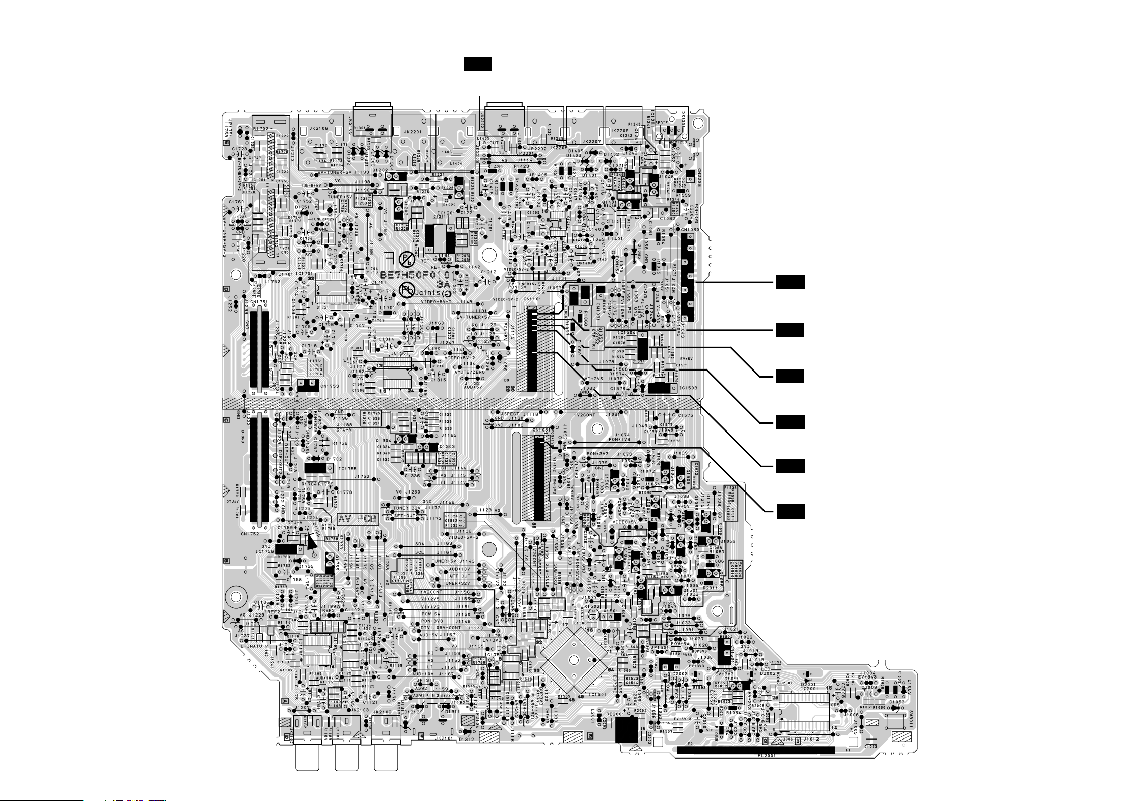
AV CBA Bottom View
WF3
C1418
PLUS LEAD
WF4
WF6
PIN 3 OF
CN1101
WF5
PIN 5 OF
CN1101
WF1
PIN 7 OF
CN1101
WF2
WF5
PIN 9 OF
CN1101
WF6
WF4
PIN 17 OF
CN1101
WF7
WF7
PIN 3 OF
CN1051
1-10-17
BE7H50F01013A
Page 41
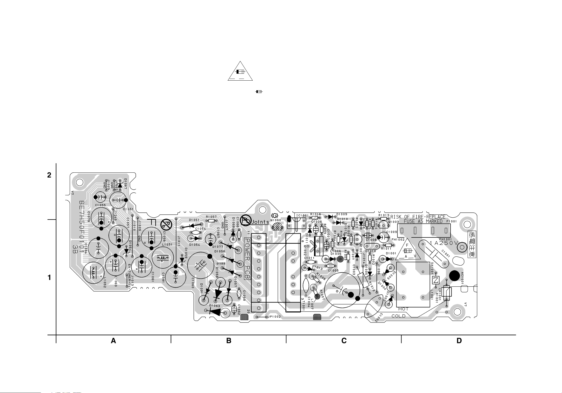
Power Supply CBA Top View
NOTE:
The voltage for parts in hot circuit is measured using
hot GND as a common terminal.
Because a hot chassis ground is present in the power
supply circut, an isolation transformer must be used.
Also, in order to have the ability to increase the input
slowly, when troubleshooting this type power supply
circuit, a variable isolation transformer is required.
CAUTION !
Fixed voltage (or Auto voltage selectable) power supply circuit is used in this unit.
If Main Fuse (F1001) is blown , check to see that all components in the power supply
circuit are not defective before you connect the AC plug to the AC power supply.
Otherwise it may cause some components in the power supply circuit to fail.
F
A V
CAUTION !
For continued protection against fire hazard,
replace only with the same type fuse.
ATTENTION : Pour une protection continue les risqes
d'Incele n'utiliser que des fusible de même type.
Risk of fire-replace fuse as marked.
"This symbol means fast operating fuse."
"Ce symbole reprèsente un fusible à fusion rapide."
1-10-18
BE7H50F01013B
Page 42
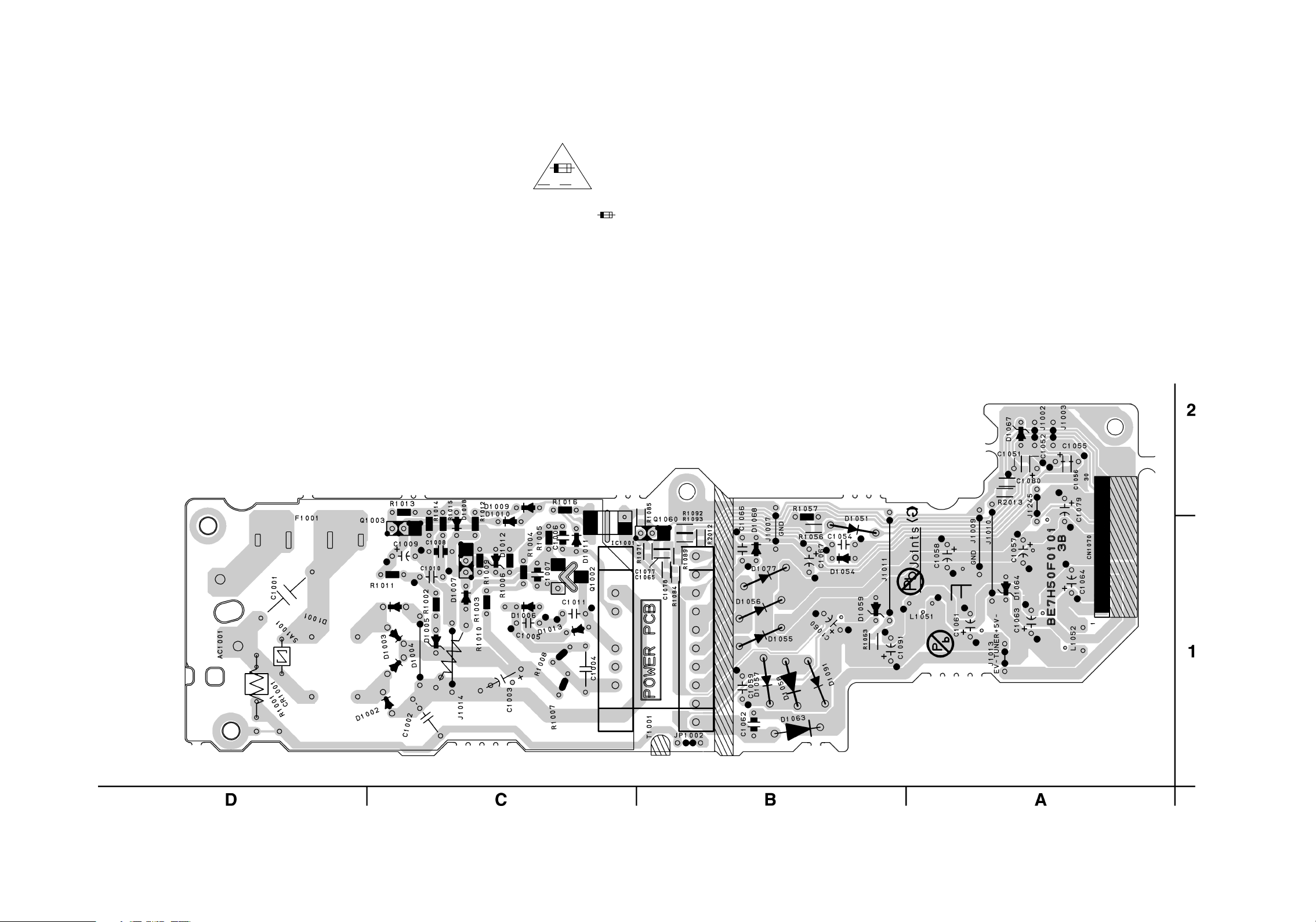
Power Supply CBA Bottom View
NOTE:
The voltage for parts in hot circuit is measured using
hot GND as a common terminal.
Because a hot chassis ground is present in the power
supply circut, an isolation transformer must be used.
Also, in order to have the ability to increase the input
slowly, when troubleshooting this type power supply
circuit, a variable isolation transformer is required.
CAUTION !
Fixed voltage (or Auto voltage selectable) power supply circuit is used in this unit.
If Main Fuse (F1001) is blown , check to see that all components in the power supply
circuit are not defective before you connect the AC plug to the AC power supply.
Otherwise it may cause some components in the power supply circuit to fail.
F
A V
CAUTION !
For continued protection against fire hazard,
replace only with the same type fuse.
ATTENTION : Pour une protection continue les risqes
d'Incele n'utiliser que des fusible de même type.
Risk of fire-replace fuse as marked.
"This symbol means fast operating fuse."
"Ce symbole reprèsente un fusible à fusion rapide."
1-10-19
BE7H50F01013B
Page 43
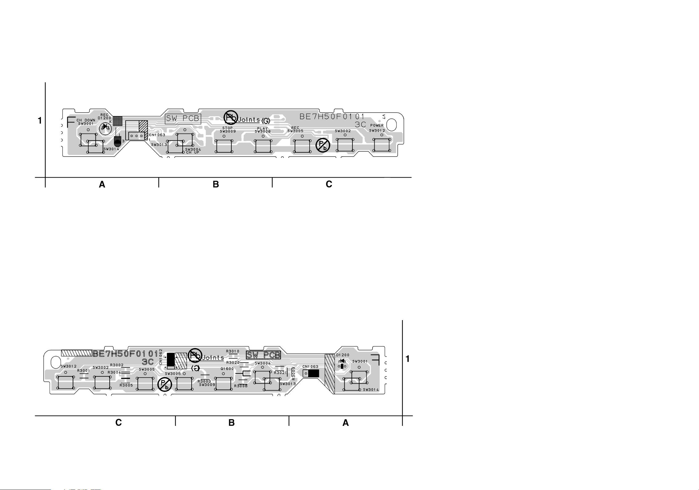
SW CBA Top View
SW CBA Bottom View
1-10-20
BE7H50F01013C
Page 44
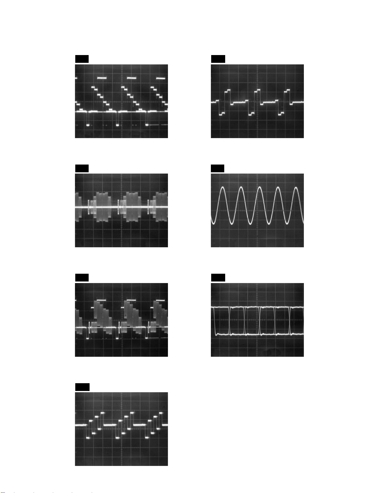
WF1
Pin 7 of CN1101
WAVEFORMS
WF5
Pin 5 of CN1101
VIDEO-Y 0.2V 20µsec
WF2
Pin 9 of CN1101
VIDEO-C 0.2V 20
WF3
C1418 PLUS LEAD
VIDEO-Cr
WF6
Pin 17 of CN1101
µ
sec
AUDIO(L)-OUT
WF7
Pin 3 of CN1051
0.2V 20µsec
1V 0.5ms
VIDEO-CVBS 0.5V 20
WF4
Pin 3 of CN1101
VIDEO-Cb
0.2V 20µsec
µ
µ
sec
SPDIF 1V 0.1
sec
NOTE:
Input: COLOR BAR SIGNAL
(WITH 1KHz AUDIO SIGNAL)
1-11-1
RD4NWF
Page 45
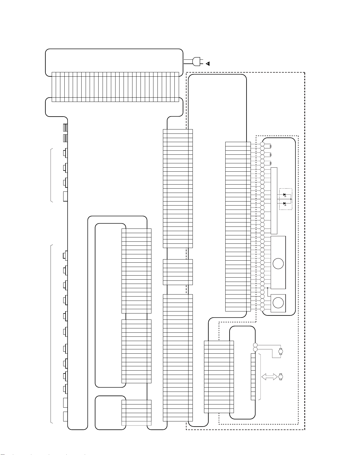
WIRING DIAGRAM
EV+10.5V 11
CN1060 CN1070
FRONT
DIGITAL
REAR
EV+10.5V 33
EV+10.5V 22
GND 44
ANT
-OUT
ANT
-IN
VIDEO
-IN2
AUDIO(R)
-IN2
AUDIO(L)
-IN2
S-VIDEO
IN2
AUDIO OUT
(COAXIAL)
AUDIO(R)
-OUT1
AUDIO(L)
-OUT1
AUDIO(R)
-IN1
AUDIO(L)
-IN1
VIDEO-Pr/Cr
OUT
VIDEO-Pb/Cb
OUT
VIDEO-Y
OUT
VIDEO
-OUT
VIDEO
-IN1
S-VIDEO
OUT
S-VIDEO
IN1
POWER
SUPPLY
CBA
1515
GND 1717
EV+5V 99
GND 55
EV+5V 66
+5V-L 1111
+5V-L 1212
GND 1313
GND 1414
GND
+5V-L 1010
EV+5V 77
EV+5V 88
GND 1616
TUNER+32V 2121
EV+14V 1919
EV+2.8V 2222
GND 1818
EV+14V 2020
AV CBA
NU
DTV1.05V-CONT
GND 33
P-ON+3.3V 44
P-ON+2.5V 55
P-ON+2.8V 66
NU
GND 88
DIF-AGC 99
GND 1010
DIF-OUT1 1111
CN102
DIF-OUT2 1212
GND 1313
DTV-VIDEO 1414
DTV-AUDIO(L) 1515
DTV-AUDIO(R)
GND 1717
NU 1818
NU 1919
NU 2020
SW CBA
CN101
CN1062
GND
NU 22
TUNER+5V 33
TU-SCL 44
TU-SDA 55
GND 66
DTV-S-SREQ 77
DTV-S-SCLK 88
DTV-S-SIN 99
DTV-S-SOUT 1010
GND 1111
DTV-S-RESET 1212
GND 1313
SDA 1414
SCL 1515
NU 11
NU 22
KEY-1 33
GND 44
KEY-2 55
NU 66
DTV MODULE CBA UNIT
1616
EV+2.8V 2727
EV+2.8V 2525
NU 2828
NU 2929
NU 3030
EV+2.8V 2626
EV+2.8V 2323
EV+2.8V 2424
SUB-RXD 3030
RDY 2929
SUB-TXD 2828
SYS-RESET 2727
SUB-SCLK 2626
GND 2525
GND 2424
GND 2323
VIDEO-C-IN 2222
GND 2121
11
22
77
11
CN1752
CN1751
CN1061
CN1101
CN1753
CN1051
VIDEO-Y/CVBS-IN
AUDIO+5V 1919
DVD-AUDIO-MUTE
AUDIO(L)-OUT
GND
AUDIO(R)-OUT
GND
AUDIO(R)-IN 1313
GND 1212
AUDIO(L)-IN 1111
GND
VIDEO-C-OUT 99
GND 88
VIDEO-Y(I/P)-OUT
GND 66
VIDEO-Pr/Cr-OUT
GND
VIDEO-Pb/Cb-OUT
GND 11
DTV-S-RESET 22
DTV-S-SOUT 33
DTV-S-SIN 44
DTV-S-SCLK 55
DTV-S-SREQ 66
GND30
GND29
GND28
EV+10.5V27
EV+10.5V26
EV+10.5V25
GND24
GND23
P-ON+5V22
P-ON+5V21
P-ON+5V20
GND19
GND18
P-ON+3.3V17
P-ON+3.3V16
P-ON+3.3V15
GND14
GND13
EV+2.8V12
EV+2.8V11
EV+2.8V10
GND9
GND8
P-ON+1.8V7
P-ON+1.8V6
GND5
GND4
SPDIF3
GND 22
1V2CONT 11
2020
1818
1717
1616
1515
1414
1010
77
55
44
33
30
29
28
27
26
25
24
23
22
21
20
19
18
17
16
15
14
13
12
11
10
9
8
7
6
5
4
3
AC CORD
LDD-IIN4
LDD-IIN3
LDD-IIN2
LDD-IINR
LDD-VDD
CN701
DVD MAIN CBA UNIT
CN501
SW1
17 2
SL(-)
16 3
SL(+)
15 4
GND
14 5
T-SCN2
13 6
CN101
T-SCN3
12 7
VH(-)
11 8
HW(-)
10 9
910
HW(+)
CN301
HV(-)
811
HV(+)
712
HU(-)
613
HU(+)
514
VCC
415
U
316
V
217
118
W
LDD-VDD
LDD-ENABLE
LDD-OSCEN
LDD-WEN4
LDD-WEN3
LDD-WEN2
CN201
LDD-SEL1
PD-VSW
PD/FSPD-VCC
FSPD-VC
FSPD-VSW
FSPD-VOUT
FCS(+)
TRK(+)
TRK(-)
GND
GND
GND
PD-VC
RF(+)
RF(-)
GND
GND
CN1001
1
2FCS(-)
3
4
5TILT(+)
6TILT(-)
7
8
9
10
NU
11
12
13
14
15
16
17
18
19
20
21
22
23
24
F
25
G
26
H
27
E
28
29
30
A
31
B
32
C
33
D
34
35
36
37
38
39
40
RELAY CBA
CN1002
FOCUS
ACTUATOR
TRACKING
ACTUATOR
TILT
ACTUATOR
DVD-LD
CD-LD
DVD/CD LASER DIODE DRIVE
DVD MECHANISM & DVD MAIN CBA ASSEMBLY
PICKUP
PDIC
FPDIC
1
2
3
4
5
6
7
8
9
10
11
M
M
SLED
MOTOR
SPINDLE
MOTOR
DVD MECHANISM
1-12-1
E7H50WI
Page 46
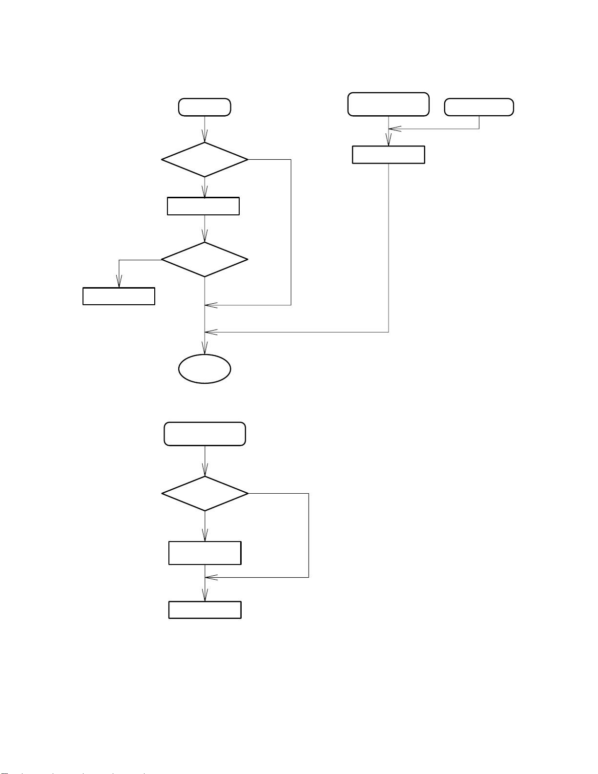
SYSTEM CONTROL TIMING CHARTS
Tray ejection
No
Power on
INNER-SW
open?
No
Tray insertion
INNER-SW
open?
Yes
To disc
distinction
Yes
[ Tray Open ]
button is pressed.
Tray insertion
Push Close
[ Tray Open ]
button is pressed.
INNER-SW
open?
Yes
SLED
moves
Tray ejection
No
1-13-1 R4NTI
Page 47
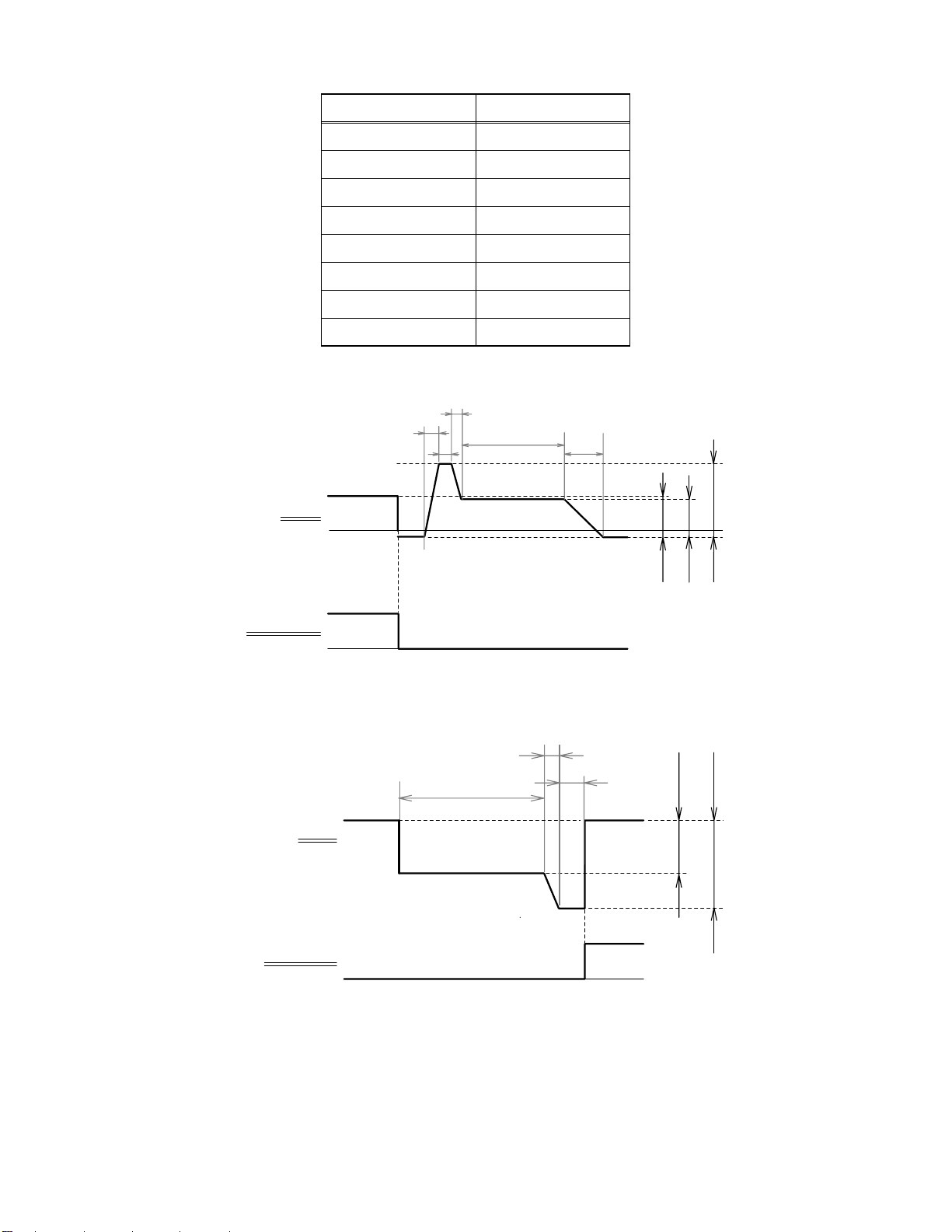
Parameter
Tray open
Tray ejection direction
SLED
V*: Voltage T*: Eve n t tim er
V0: 2.40 V T1: 0.050 s
V1: 4.25 V T2: 2.000 s
V2: 2.00 V T3: 0.008 s
V3: 2.36 V T4: 0.006 s
V4: 4.26 V T5: 0.066 s
T6: 1.500 s
T7: 0.800 s
T8: 0.005 s
T4
T3
T1
T2
T5
Tray close
Tray insertion direction
open
INNER-SW
close
Tray ejection direction
SLED
Tray insertion direction
open
INNER-SW
close
T6
T8
T7
V0
V3
V2
V1
V4
1-13-2 R4NTI
Page 48
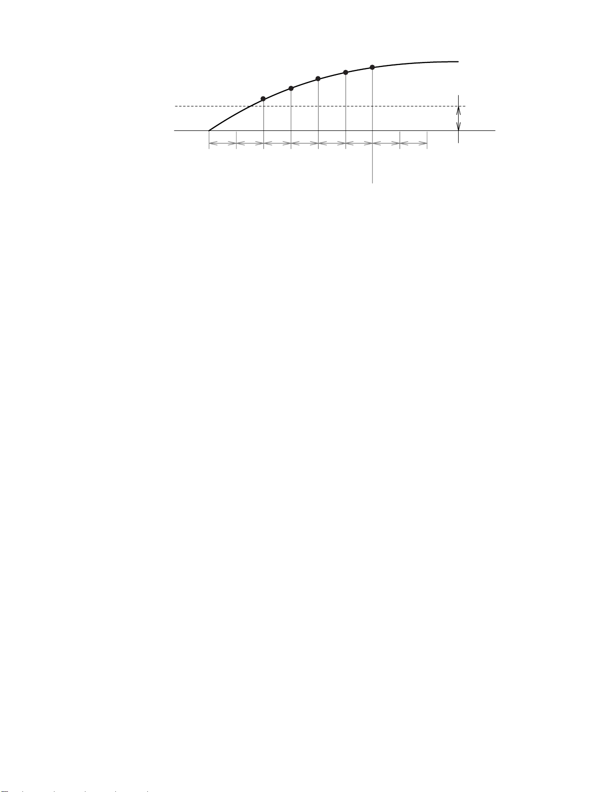
Push close
Threshold level
0.08 V
0.02 s
Push Close
detection
1-13-3 R4NTI
Page 49
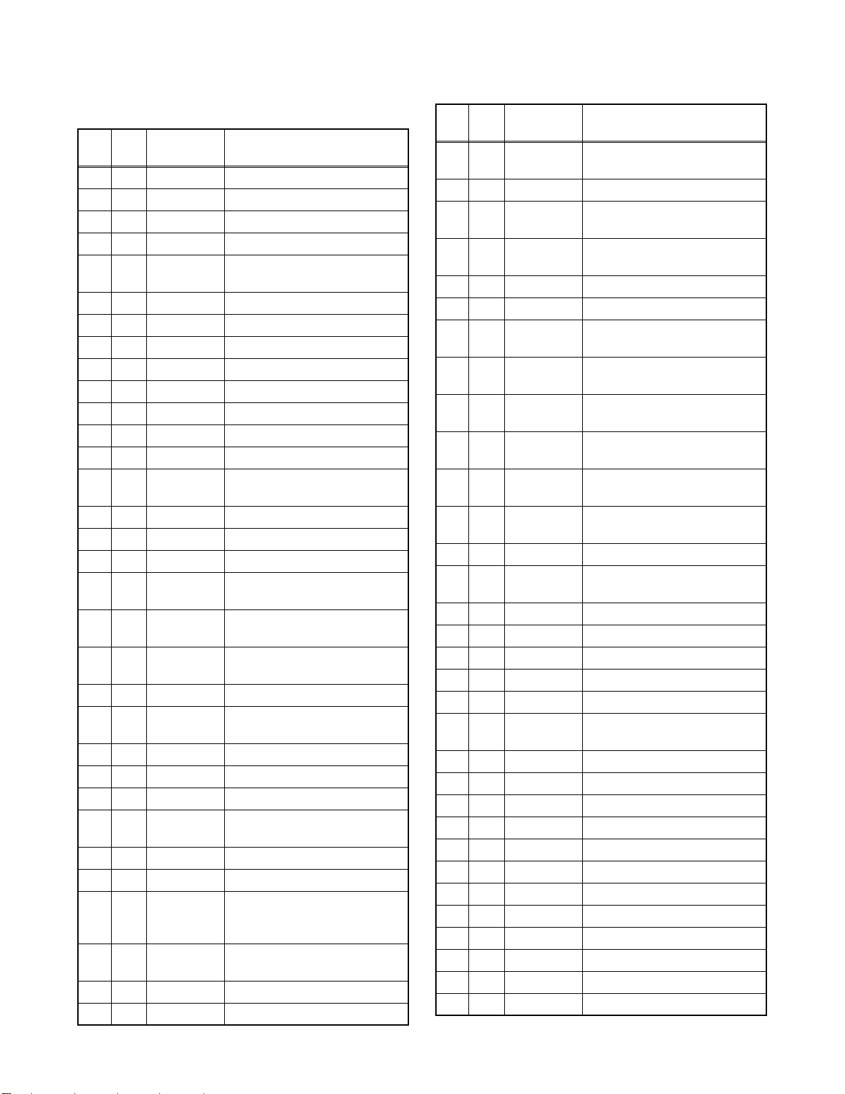
IC PIN FUNCTION DESCRIPTIONS
IC1501 (SUB MICRO CONTROLLER)
Pin
IN/
No.
OUT
1 IN KEY-1 Key Data Input 1
2 IN KEY-2 Key Data Input 2
3 IN POW-SW Abnormal Voltage Detection
4 IN AFT Tuner Voltage Input Signal
56 IN VCC +3.3V Power Supply
7 IN VCC +3.3V Power Supply
8 OUT XOUT Main Clock Output
9 IN XIN Main Clock Input
10 - GND Ground
11 IN XCIN Sub Clock Input
12 OUT XCOUT Sub Clock Output
13 - GND Ground
14 IN RESET
15 - NU Not Used
16 - NU Not Used
17 - NU Not Used
18 OUT SUB-TXD
19 IN SUB-RXD
20 OUT SUB-SCLK
21 - NU Not Used
22 OUT
23 - NU Not Used
24 - NU Not Used
25 - NU Not Used
26 OUT 1V2CONT
27 IN REMOTE Remote Signal Input
28 - NU Not Used
29 IN RDY
30 IN P-DOWN
31 OUT FL-SEL FL Select (Low Level)
32 - NU Not Used
Signal
Name
FLASHVPP
SYSRESET
Function
Flash Writing Voltage
Micro Controller Reset
Signal
Transmission Data to Main
Micro Controller
Reception Data from Main
Micro Controller
Communication Clock with
Main Micro Controller
System Reset Signal
Power Regulator Control
Signal
Ready/Busy communication
Control with Main Micro
Controller
Power Voltage Down
Detector Signal
Pin
IN/
No.
OUT
IN/
33
OUT
34 OUT SCL Serial Clock
IN/
35
OUT
36 OUT
37 - NU Not Used
38 - NU Not Used
39 OUT
40 OUT
41 OUT
42 OUT
43 OUT
44 OUT
45 - NU Not Used
46 OUT
47 - NU Not Used
48 - NU Not Used
49 - NU Not Used
50 - NU Not Used
51 - NU Not Used
52 OUT
53 OUT PWSW Power On Signal Output
54 - NU Not Used
55 - NU Not Used
56 - NU Not Used
57 - NU Not Used
58 OUT LED3
59 OUT LED2 Recording LED Control Signal
60 OUT LED1
61 - GND Ground
62 - NU Not Used
63 - NU Not Used
64 - NU Not Used
Signal
Name
SDA Serial Data
FLASHSDA
FLASHSCL
AUDIOSW2
AUDIOSW1
VIDEOSW1
VIDEOSW2
VIDEOSW3
VIDEOMUTE
DTV1.05VCONT
REGCONT
Serial Data Signal for Flash
Serial Clock Signal for Flash
Audio Input Select Signal 2
Audio Input Select Signal 1
Video Input Select Signal 1
Video Input Select Signal 2
Video Input Select Signal 3
Video Mute Control Signal
DTV1.05 Control Signal
Power Regulator Control
Signal
Timer LED Control Signal
Power LED Control Signal
Function
1-14-1 E7H50PIN
Page 50
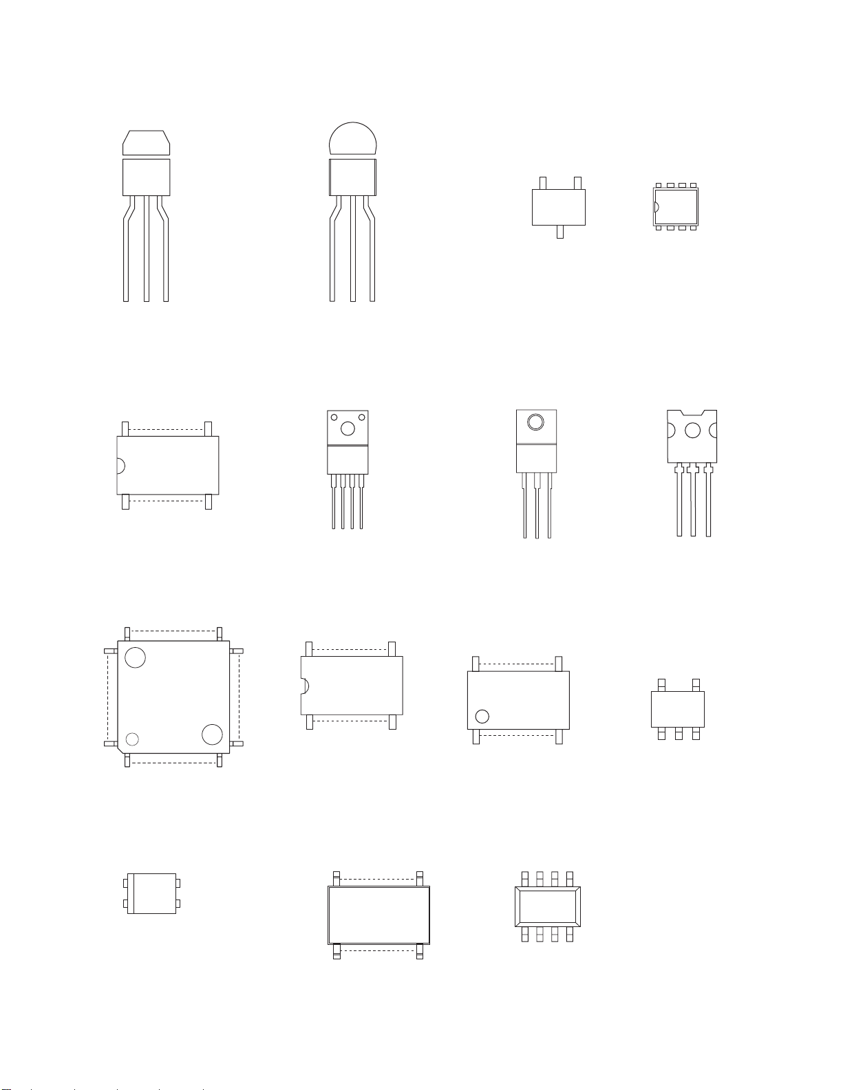
LEAD IDENTIFICATIONS
ECB
24
1
KRC103M-AT/P
KTA1267-GR-AT/P
KTC3199-(BL,GR)-AT/P
13
12
ECB
PQ070XF01SZHMM1697AJBE
1234
KTA1271-Y-AT/P
KTC3205-Y-AT/P
RN1402
KIA4558P/P
KRC102S-RTK/P
BE
C
85
14
2SK3563(Q) KTB1151-Y-U/P
GDS
E C B
MN101C77AFP1
48
49
64
1
1
2
33
16
1: Anode
4
2: Cathode
3
3: Emitter
4: Collector
32
17
AN5832SA-E1V
32
1
UTC4580E
1
17
16
CD4052BNSR
MM1637XVBE
BU4219G-TR
R3112N191A-TR-FA
R3112N191A-TR-FB
16
9
PST3619NR
54
1
8
123
Note:
M24128-BWMN6TPPS2561A-1(W)
58
85
A: Anode
K: Cathode
E: Emitter
C: Collector
B: Base
R: Reference
G: Gate
14
4
D: Drain
S: Source
1-15-1 E7H50LE
Page 51
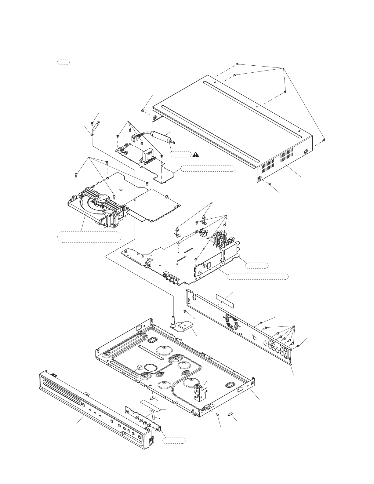
Cabinet
EXPLODED VIEWS
See Electrical Parts List
for parts with this mark.
Some Ref. Numbers are
not in sequence.
2L030
2B49
2L050
DVD Mechanism &
DVD Main CBA Assembly
2L010
2L010
2L041
A28
AC1001
POWER SUPPLY CBA
A3
2L010
2B10
2L040
A1X
A23
A5
2B22
SW CBA
A8
2L044
2B15
2B11
AV CBA
DTV MODULE CBA UNIT
A6
2L011
2L020
2L012
A4
A2
A5
2L042
1-16-1 E7H50CEX
Page 52
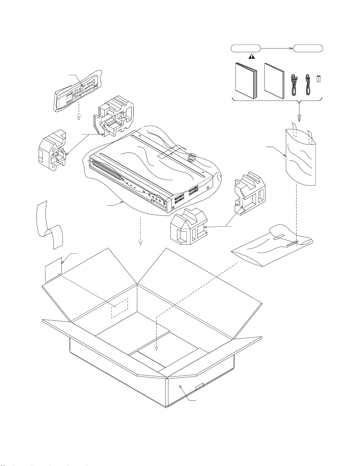
Packing
X1
S2
Unit
Upper Side Lower Side
X20
X4
X22
X3
X5 X2
A8
S3
S2
Some Ref. Numbers
are not in sequence.
S1
1-16-2 E7H50PEX
Page 53
MECHANICAL PARTS LIST
PRODUCT SAFETY NOTE: Products marked with a
# have special characteristics important to safety.
Before replacing any of these components, read
carefully the product safety notice in this service
manual. Don't degrade the safety of the product
through improper servicing.
NOTE: Parts that are not assigned part numbers
(---------) are not available.
Ref. No. Description Part No.
A1X FRONT ASSEMBLY E7H50UD 1VM222941
A2 CHASSIS E7C40UD 1VM121059G
A3 TOP COVER(BLACK) E7C50UD 1VM323571
A4 REAR PANEL E7H50UD 1VM222839
A5 FOO T H5100UD 0VM406940A
A6 MODEL NO LABEL E7H50UD ---------A8 RFID LABEL(NO PRINTING) E9A80UD ---------A23 PCB CUSHION E7C40UD 1VM425421A
A28 HOLDER EAS(H9410UD) MAKER
2B10 PCB SUPPORT/PCB SP A CERS KGLS-14S XP0U027WD001
2B11 FRONT BRACKET R E2A00JD 1VM424123F
2B15 MAIN PCB HOLDER E2B10ED 1VM323176A
2B22 HIMELON T APE(30*5) E7C40UD 1VM425436
2B49 M-PCB PLA TE EARTH E6700UD 1VM421132
2L010 SCREW T AP TIGHT M3X5 BIND HEAD+BLK NI GBHC3050
2L011 SCREW C-TIGHT M3X5 BIND HEAD + GBCC3050
2L012 SCREW C-TIGHT M3X5 BIND HEAD + GBCC3050
2L020 SCREW B-TIGHT M3X8 BIND HEAD+ GBHB3080
2L030 SCREW P-TIGHT 3X10 BIND HEAD+ GBJP3100
2L040 SCREW S-TIGHT M3X6 BIND HEAD+ GBJS3060
2L041 SCREW S-TIGHT M3X6 BIND HEAD+ GBJS3060
2L042 SCREW S-TIGHT M3X6 BIND HEAD+ GBJS3060
2L044 SCREW S-TIGHT M3X6 BIND HEAD+ GBJS3060
2L050 SCREW S-TIGHT M3X10 BIND HEAD+ GBJS3100
NO.EM150DR
PACKING
S1 GIFT BOX CARTON E7C50UD 1VM323585A
S2 SIDE PAD E7C40UD 1VM121069
S3 UNIT BAG E5500UD 0VM411683
ACCESSORIES
X1 REMOTE CONTROL UNIT NB553UD NB553UD
X2 BATTER Y R03-B500/01S XB0M451CZB01
X3 RF CABLE 2.5C-2V WPZ0901TM002
X4 ACCESSORY BAG E5795ED 0VM41605 9
X5 AV CORD 1000/BLA CK WPZ0102TM018
X20# OWNERS MANU AL E7H50UD 1VMN23411
X22 QUICK GUIDE E7H50UD 1VMN23412
0VM415877
20070313 1-17-1 E7H50CA
Page 54
ELECTRICAL PARTS LIST
PRODUCT SAFETY NOTE: Products marked with a
# have special characteristics important to safety.
Before replacing any of these components, read
carefully the product safety notice in this service
manual. Don't degrade the safety of the product
through improper servicing.
NOTES:
1. Parts that are not assigned part numbers (---------)
are not available.
2. Tolerance of Capacitors and Resistors are noted
with the following symbols.
C.....±0.25% D.....±0.5% F.....±1%
G.....±2% J......±5% K.....±10%
M.....±20% N.....±30% Z.....+80/-20%
DVD MECHANISM & D VD MAIN CBA
ASSEMBLY
Ref. No. Description Part No.
DVD MECHANISM & D VD MAIN CBA
ASSEMBL Y
N78F0DUN
DTV MODULE CBA UNIT
Ref. No. Description Part No.
DTV MODULE CBA UNIT 1VSA15405
AV ASSEMBLY
Ref. No. Description Part No.
AV ASSEMBLY
Consists of the following:
AV CBA (SUB-A)
POWER SUPPLY CBA (SUB-B)
SW CBA (SUB-C)
AV CBA
Ref. No. Description Part No.
AV CBA (SUB-A)
Consists of the following:
CAPACITORS
C1068 CHIP CERAMIC CAP .( 1608) F Z 0.1µF/50V CHD1JZ30F104
C1070 ELECTROL YTIC CAP. 100µF/6.3V M CE0KMASDL101
C1074 ELECTROL YTIC CAP. 100µF/6.3V M CE0KMASDL101
C1075 CHIP CERAMIC CAP .( 1608) F Z 0.1µF/50V CHD1JZ30F104
C1076 ELECTROL YTIC CAP. 100µF/6.3V M CE0KMASDL101
C1081 CHIP CERAMIC CAP .( 1608) F Z 0.1µF/50V CHD1JZ30F104
C1082 ELECTROL YTIC CAP. 100µF/6.3V M CE0KMASDL101
C1101 CHIP CERAMIC CAP .( 1608) F Z 0.1µF/50V CHD1JZ30F104
C1102 ELECTROL YTIC CAP. 100µF/6.3V M CE0KMASDL101
C1121 ELECTROL YTIC CAP. 10µF/16V M CE1CMASDL100
C1122 ELECTROL YTIC CAP. 10µF/16V M CE1CMASDL100
C1123 CHIP CERAMIC CAP .(1608) CH J 33pF/50V CHD1JJ3CH330
C1124 CHIP CERAMIC CAP .(1608) CH J 33pF/50V CHD1JJ3CH330
C1125 CHIP CERAMIC CAP .( 1608) F Z 0.1µF/50V CHD1JZ30F104
C1135 ELECTROL YTIC CAP. 220µF/16V M CE1CMASDL221
1VSA15451
----------
----------
----------
----------
Ref. No. Description Part No.
C1152 ELECTROL YTIC CAP. 100µF/16V M CE1CMASDL101
C1171 CHIP CERAMIC CAP .(1608) CH J 1000pF/50V CHD1JJ3CH102
C1172 CHIP CERAMIC CAP .(1608) CH J 1000pF/50V CHD1JJ3CH102
C1175 ELECTROL YTIC CAP. 10µF/16V M CE1CMASDL100
C1176 ELECTROL YTIC CAP. 10µF/16V M CE1CMASDL100
C1181 CHIP CERAMIC CAP .(1608) CH J 1000pF/50V CHD1JJ3CH102
C1182 CHIP CERAMIC CAP .(1608) CH J 1000pF/50V CHD1JJ3CH102
C1185 ELECTROL YTIC CAP. 10µF/16V M CE1CMASDL100
C1186 ELECTROL YTIC CAP. 10µF/16V M CE1CMASDL100
C1201 ELECTROL YTIC CAP. 10µF/16V M CE1CMASDL100
C1202 ELECTROL YTIC CAP. 10µF/16V M CE1CMASDL100
C1203 CHIP CERAMIC CAP .(16 08) CH J 470pF/50V CHD1JJ3CH471
C1204 CHIP CERAMIC CAP .(16 08) CH J 470pF/50V CHD1JJ3CH471
C1205 CHIP CERAMIC CAP .(1608) CH J 68pF/50V CHD1JJ3CH680
C1206 CHIP CERAMIC CAP .(1608) CH J 68pF/50V CHD1JJ3CH680
C1211 CHIP CERAMIC CAP . (1608) F Z 0.1µF/50V CHD1JZ30F104
C1212 ELECTROL YTIC CAP. 470µF/6.3V M CE0KMASDL471
C1221 ELECTROL YTIC CAP. 10µF/16V M CE1CMASDL100
C1222 ELECTROL YTIC CAP. 10µF/16V M CE1CMASDL100
C1241 CHIP CERAMIC CAP . (1608) F Z 0.1µF/50V CHD1JZ30F104
C1247 CHIP CERAMIC CAP.(1608) B K 1µF/10V CHD1AK30B105
C1301 CHIP CERAMIC CAP . (1608) F Z 0.1µF/50V CHD1JZ30F104
C1302 CHIP CERAMIC CAP . (1608) F Z 0.1µF/50V CHD1JZ30F104
C1303 CHIP CERAMIC CAP . (1608) F Z 0.1µF/50V CHD1JZ30F104
C1304 CHIP CERAMIC CAP . (1608) F Z 0.1µF/50V CHD1JZ30F104
C1305 CHIP CERAMIC CAP . (1608) F Z 0.1µF/50V CHD1JZ30F104
C1306 CHIP CERAMIC CAP . (1608) F Z 0.1µF/50V CHD1JZ30F104
C1313 CHIP CERAMIC CAP.(1608) B K 0.01µF/50V CHD1JK30B103
C1314 ELECTROL YTIC CAP. 22µF/16V M CE1CMASDL220
C1315 ELECTROL YTIC CAP. 100µF/6.3V M CE0KMASDL101
C1316 CHIP CERAMIC CAP . (1608) F Z 0.1µF/50V CHD1JZ30F104
C1331 CHIP CERAMIC CAP .(1608) CH J 33pF/50V CHD1JJ3CH330
C1332 CHIP CERAMIC CAP .(1608) CH J 33pF/50V CHD1JJ3CH330
C1333 CHIP CERAMIC CAP . (1608) F Z 0.1µF/50V CHD1JZ30F104
C1334 CHIP CERAMIC CAP . (1608) F Z 0.1µF/50V CHD1JZ30F104
C1335 CHIP CERAMIC CAP . (1608) F Z 0.1µF/50V CHD1JZ30F104
C1337 CHIP CERAMIC CAP . (1608) F Z 0.1µF/50V CHD1JZ30F104
C1338 ELECTROL YTIC CAP. 100µF/6.3V M NP CP0KMASNC101
C1405 CHIP CERAMIC CAP.(1608) B K 0.01µF/50V CHD1JK30B103
C1406 ELECTROL YTIC CAP. 1µF/50V M CE1JMASDL1R0
C1407 ELECTROL YTIC CAP. 1µF/50V M CE1JMASDL1R0
C1408 ELECTROL YTIC CAP. 1µF/50V M CE1JMASDL1R0
C1409 ELECTROL YTIC CAP. 22µF/16V M CE1CMASDL220
C1410 CHIP CERAMIC CAP.(1608) B K 0.01µF/50V CHD1JK30B103
C1411 CHIP CERAMIC CAP . (1608) F Z 0.1µF/50V CHD1JZ30F104
C1413 CHIP CERAMIC CAP . (1608) F Z 0.1µF/50V CHD1JZ30F104
C1414 CHIP CERAMIC CAP . (1608) F Z 0.1µF/50V CHD1JZ30F104
C1415 ELECTROL YTIC CAP. 100µF/6.3V M CE0KMASDL101
C1417 CHIP CERAMIC CAP . (1608) F Z 0.1µF/50V CHD1JZ30F104
C1418 ELECTROL YTIC CAP. 470µF/6.3V M CE0KMASDL471
C1419 ELECTROL YTIC CAP. 1000µF/6.3V M CE0KMASDL102
C1420 ELECTROL YTIC CAP. 470µF/6.3V M CE0KMASDL471
C1421 ELECTROL YTIC CAP. 470µF/6.3V M CE0KMASDL471
C1501 ELECTROL YTIC CAP. 1000µF/6.3V M CE0KMASDL102
C1502 CHIP CERAMIC CAP . (1608) F Z 0.1µF/50V CHD1JZ30F104
C1503 CHIP CERAMIC CAP . (1608) F Z 0.1µF/50V CHD1JZ30F104
C1506 CHIP CERAMIC CAP .(1608) CH J 22pF/50V CHD1JJ3CH220
C1507 CHIP CERAMIC CAP . CH J 18pF/50V CHD1JJ3CH180
C1508 CHIP CERAMIC CAP.(1608) B K 0.1µF/25V CHD1EK3 0B104
20070313 1-18-1 E7H50EL
Page 55
Ref. No. Description Part No.
If C1509 is 0.015µF, then IC1502 is R3112N191A-TR-FA, R3112N191A-TR-FB or
BU4219G-TR.
C1509 CHIP CERAMIC CAP . (1608) B K 0.015µF/50V CHD1JK30B153
IC1502 VOLTAGE DETECT R3112N191A-TR-FA QSZBA0TRC021
IC1502 VOLTAGE DETECT R3112N191A-TR-FB QSZBA0TRC022
IC1502 RESET IC BU4219G-TR QSZBA0TRM090
If C1509 is 0.1µF, then IC15 02 is PS T3619NR .
C1509 CHIP CERAMIC CAP . (1608) B K 0.1µF/25V CHD1EK30B104
IC1502 SYSTEM RESET IC PST3619NR QSZBA0TMM151
C1510 CHIP CERAMIC CAP . (1608) B K 1000pF/50V CHD1JK30B102
C1511 CHIP CERAMIC CAP .( 1608) F Z 0.1µF/50V CHD1JZ30F104
C1512 CHIP CERAMIC CAP .(1608) CH J 100pF/50V CHD1JJ3CH101
C1513 CHIP CERAMIC CAP .(1608) CH J 100pF/50V CHD1JJ3CH101
C1520 CHIP CERAMIC CAP .( 1608) F Z 0.1µF/50V CHD1JZ30F104
C1575 ELECTROL YTIC CAP. 100µF/6.3V M(105C) CE0KMASTH101
C1576 ELECTROL YTIC CAP. 100µF/6.3V M(105C) CE0KMASTH101
C1577 CHIP CERAMIC CAP .( 1608) F Z 0.1µF/50V CHD1JZ30F104
C1578 CHIP CERAMIC CAP .( 1608) F Z 0.1µF/50V CHD1JZ30F104
C1701 ELECTROL YTIC CAP. 4.7µF/50V M CE1JMASDL4R7
C1702 ELECTROL YTIC CAP. 2.2µF/50V M CE1JMASDL2R2
C1703 ELECTROL YTIC CAP. 2.2µF/50V M CE1JMASDL2R2
C1704 ELECTROL YTIC CAP. 2.2µF/50V M CE1JMASDL2R2
C1705 ELECTROL YTIC CAP. 10µF/16V M CE1CMASDL100
C1706 ELECTROL YTIC CAP. 3.3µF/50V M CE1JMASDL3R3
C1707 ELECTROL YTIC CAP. 3.3µF/50V M CE1JMASDL3R3
C1708 CHIP CERAMIC CAP .( 1608) F Z 0.1µF/50V CHD1JZ30F104
C1709 CHIP CERAMIC CAP . (1608) B K 0.022µF/50V CHD1JK30B223
C1710 ELECTROL YTIC CAP. 2.2µF/50V M CE1JMASDL2R2
C1711 CHIP CERAMIC CAP .( 1608) F Z 0.1µF/50V CHD1JZ30F104
C1713 CHIP CERAMIC CAP . (1608) B K 0.1µF/25V CHD1EK30B104
C1714 CHIP CERAMIC CAP . (1608) B K 0.1µF/25V CHD1EK30B104
C1715 ELECTROL YTIC CAP. 0.33µF/50V M CE1JMASDLR33
C1716 CHIP CERAMIC CAP .(1608) CH J 1000pF/50V CHD1JJ3CH102
C1718 ELECTROL YTIC CAP. 1µF/50V M CE1JMASDL1R0
C1719 ELECTROL YTIC CAP. 1µF/50V M CE1JMASDL1R0
C1720 CHIP CERAMIC CAP . (1608) B K 0.033µF/50V CHD1JK30B333
C1721 CHIP CERAMIC CAP . (1608) B K 0.1µF/25V CHD1EK30B104
C1723 ELECTROL YTIC CAP. 100µF/6.3V M CE0KMASDL101
C1724 CHIP CERAMIC CAP .( 1608) F Z 0.1µF/50V CHD1JZ30F104
C1725 CHIP CERAMIC CAP .( 1608) F Z 0.1µF/50V CHD1JZ30F104
C1747 CHIP CERAMIC CAP . (1608) B K 0.033µF/50V CHD1JK30B333
C1749 CHIP CERAMIC CAP .(1608) CH J 47pF/50V CHD1JJ3CH470
C1750 CHIP CERAMIC CAP .(1608) CH J 22pF/50V CHD1JJ3CH220
C1751 CHIP CERAMIC CAP .( 1608) F Z 0.1µF/50V CHD1JZ30F104
C1752 ELECTROL YTIC CAP. 1000µF/6.3V M CE0KMASDL102
C1753 CHIP CERAMIC CAP .( 1608) F Z 0.1µF/50V CHD1JZ30F104
C1754 ELECTROL YTIC CAP. 1µF/50V M CE1JMASDL1R0
C1755 CHIP CERAMIC CAP . (1608) B K 0.01µF/50V CHD1JK30B103
C1756 CHIP CERAMIC CAP . (1608) B K 0.01µF/50V CHD1JK30B103
C1757 ELECTROL YTIC CAP. 100µF/6.3V M CE0KMASDL101
C1760 ELECTROL YTIC CAP. 100µF/6.3V M CE0KMASDL101
C1761 ELECTROL YTIC CAP. 10µF/16V M CE1CMASDL100
C1762 ELECTROL YTIC CAP. 10µF/16V M CE1CMASDL100
C1764 CHIP CERAMIC CAP .( 1608) F Z 0.1µF/50V CHD1JZ30F104
C1766 CHIP CERAMIC CAP . F Z 0.01µF/50 V CHD1JZ30F103
C1767 CHIP CERAMIC CAP .( 1608) F Z 0.1µF/50V CHD1JZ30F104
C2002 CHIP CERAMIC CAP .(1608) CH J 100pF/50V CHD1JJ3CH101
C2003 CHIP CERAMIC CAP .( 1608) F Z 0.1µF/50V CHD1JZ30F104
C2004 ELECTROL YTIC CAP. 100µF/6.3V M CE0KMASDL101
CONNECTORS
CN1051 30PIN FFC WX1E7H50-0 03 WX1E7 H50-0 03
CN1060 FFC CONNECTOR 30PIN IMSA-9615S-30A-
PP-A
JC96J30ER0 07
Ref. No. Description Part No.
CN1061 FFC CONNECTOR IMSA-9615S-06A-PP-A JC96J06ER007
CN1101 28PIN FFC WX1E7H50-0 02 WX1E7 H50-0 02
CN1700 6PIN FFC WX1E7H50-005 WX1E7H50-005
CN1753 FFC CONNECTOR IMSA-9615S-06A-PP-A JC96J06ER007
DIODES
D1060 SWITCHING DIODE 1SS133 (T-77) QDTZ001SS133
D1061 SWITCHING DIODE 1SS133 (T-77) QDTZ001SS133
D1062 ZENER DIODE MTZJT-774.3A QDTA0MTZJ4R3
D1065 PCB JUMPER D0.6-P10.0 JW10.0T
D1066 SWITCHING DIODE 1SS133 (T-77) QDTZ001SS133
D1070 SWITCHING DIODE 1SS133 (T-77) QDTZ001SS133
D1071 SWITCHING DIODE 1SS133 (T-77) QDTZ001SS133
D1074 SWITCHING DIODE 1SS133 (T-77) QDTZ001SS133
D1507 SWITCHING DIODE 1SS133 (T-77) QDTZ001SS133
D1508 SWITCHING DIODE 1SS133 (T-77) QDTZ001SS133
D1509 SWITCHING DIODE 1SS133 (T-77) QDTZ001SS133
D1510 PCB JUMPER D0.6-P5.0 JW5.0T
D1751 ZENER DIODE MTZJT -7733B QDTB00MTZJ33
D1753 SWITCHING DIODE 1SS133 (T-77) QDTZ001SS133
D1756 SCHOTTKY BARRIER DIODE SB340 NDQZ000SB340
D2001 LED(RED) 204HD/E NPQZ00204HDE
D2002 LED(RED) 204HD/E NPQZ00204HDE
D2003 LED(YELLOW) 204YD/E NPQZ00204YDE
ICS
IC1101 IC SWITCHING CD4052BNSR NSZBA0TTY091
IC1102 IC OP AMP UTC4580E NSZBA0T2H010
IC1201 IC OP AMP KIA4558P/P NSZBA0SJY035
IC1301 VIDEO SWITCH MM1697AJBE QSZBA0TMM150
IC1401 DRIVER FOR DVD MM1637XVBE QSZBA0TMM102
IC1501 IC MICROCONTROLLER MN101C77AFP1 QSZAB0RMS080
If IC1502 is R3112N191A-TR-FA, R3112N191A-TR-FB or BU4219G-TR, then
C1509 is 0.015µF.
IC1502 V OLTAGE DETECT R3112N191A-TR-FA QSZBA0TRC021
IC1502 V OLTAGE DETECT R3112N191A-TR-FB QSZBA0TRC022
IC1502 RESET IC BU4219G-TR QSZBA0TRM090
C1509 CHIP CERAMIC CAP.(1608) B K 0.015µF/50V CHD1JK30B153
If IC1502 is PST3619NR, then C1509 is 0.1µF.
IC1502 SYSTEM RESET IC PST3619NR QSZBA0TMM151
C1509 CHIP CERAMIC CAP.(1608) B K 0.1µF/25V CHD1EK3 0B104
IC1503 VOL TAGE REGULATOR PQ070XF01SZH QSZBA0SSH054
IC1504 VOL TAGE REGULATOR PQ070XF01SZH QSZBA0SSH054
IC1701 IC MTS DECORDER AN5832SA-E1V QSZBA0TMS003
IC1755 VOL TAGE REGULATOR PQ070XF01SZH QSZBA0SSH054
IC1757 EEP-ROM 128K M24128-BWMN6TP NSZBA0 TSS268
COILS
L1054 CHOKE COIL 22µH-K LLBD00PKV021
L1055 CHOKE COIL 22µH-K LLBD00PKV021
L1056 CHOKE COIL 22µH-K LLBD00PKV021
L1241 INDUCTOR(100µH K) LAP02TA101K LL AXKATTU101
L1242 INDUCTOR(0.47µH K) LAP02TAR47K LLAXKA TTUR47
L1401 PCB JUMPER D0.6-P5.0 JW5.0T
L1701 CARBON R ES. 1/ 4W J 3.3 Ω RCX4JA TZ03R3
L1751 CHOKE COIL 22µH-K LLBD00PKV021
L1752 BEAD INDUCTOR FBR07HA121TB-00 LLBF00ZTU021
L1753 CHOKE COIL 22µH-K LLBD00PKV021
L1754 PCB JUMPER D0.6-P5.0 JW5.0T
L1760 CHIP RES.(1608) 1/10W 0 Ω RRXAZR5Z0000
L1761 CHIP RES.(1608) 1/10W 0 Ω RRXAZR5Z0000
L1762 CHIP RES.(1608) 1/10W 0 Ω RRXAZR5Z0000
L1763 CHIP RES.(1608) 1/10W 0 Ω RRXAZR5Z0000
L1764 CHIP RES.(1608) 1/10W 0 Ω RRXAZR5Z0000
L2001 INDUCTOR(100µH K) LAP02TA101K LL AXKATTU101
20070313 1-18-2 E7H50EL
Page 56
Ref. No. Description Part No.
TRANSISTORS
Q1053 TRANSISTOR KTB1151-Y - U/P NQEY0KTB1151
Q1054 TRANSISTOR (PB FREE) KTA1271-Y-A T/P NQSYKT A1271P
Q1056 TRANSISTOR KTC3199-GR-AT/P NQS4KTC3199P
Q1057 TRANSISTOR KTC3205-Y- AT/P NQSYKTC3205P
Q1063 TRANSISTOR KTC3199-GR-AT/P NQS4KTC3199P
Q1065 TRANSISTOR (PB FREE) KTA1271-Y-A T/P NQSYKT A1271P
Q1101 TRANSISTOR KRC102S-RTK/P NQ1ZKRC102SP
Q1102 TRANSISTOR KRC102S-RTK/P NQ1ZKRC102SP
Q1201 TRANSISTOR KTC3199-GR-AT/P NQS4KTC3199P
Q1202 TRANSISTOR KTC3199-GR-AT/P NQS4KTC3199P
Q1203 TRANSISTOR KTA1267-GR-A T/P NQS1KT A1267P
Q1241 TRANSISTOR KTC3199-GR-AT/P NQS4KTC3199P
Q1303 TRANSISTOR KTC3199-GR-AT/P NQS4KTC3199P
Q1304 TRANSISTOR KTC3199-GR-AT/P NQS4KTC3199P
Q1501 TRANSISTOR KTA1267-GR-A T/P NQS1KT A1267P
Q1502 TRANSISTOR KTC3199-GR-AT/P NQS4KTC3199P
Q1505 NPN TRANSISTOR KRC103M-A T/P NQSZKRC103MP
Q1506 NPN TRANSISTOR KRC103M-A T/P NQSZKRC103MP
Q1755 NPN TRANSISTOR KRC103M-A T/P NQSZKRC103MP
RESISTORS
R1066 CHIP RES. 1/10W J 47k Ω RRXAJR5Z0473
R1067 CARBON RES. 1/4W J 180 Ω RCX4JA TZ0181
R1068 CARBON RES. 1/4W J 180 Ω RCX4JA TZ0181
R1070 CHIP RES. 1/10W J 47k Ω RRXAJR5Z0473
R1072 CARBON RES. 1/4W J 680 Ω RCX4JA TZ0681
R1073 CHIP RES. 1/10W J 47k Ω RRXAJR5Z0473
R1074 CHIP RES. 1/10W J 620 Ω RRXAJR5Z0621
R1076 CHIP RES. 1/10W J 4.7k Ω RRXAJR5Z0472
R1077 CHIP RES. 1/10W J 1.1k Ω RRXAJR5Z0112
R1087 CARBON RES. 1/4W G 1.5k Ω RCX4GA TZ0152
R1090 CHIP RES. 1/10W J 1.8k Ω RRXAJR5Z0182
R1094 CHIP RES. 1/10W J 120 Ω RRXAJR5Z0121
R1097 CARBON RES. 1/4W J 220 Ω RCX4JA TZ0221
R1101 CHIP RES.(1608) 1/10W F 68k Ω RRXAFR5H0683
R1102 CHIP RES.(1608) 1/10W F 68k Ω RRXAFR5H0683
R1103 CHIP RES.(1608) 1/10W F 68k Ω RRXAFR5H0683
R1104 CHIP RES.(1608) 1/10W F 68k Ω RRXAFR5H0683
R1105 CHIP RES.(1608) 1/10W F 68k Ω RRXAFR5H0683
R1106 CHIP RES.(1608) 1/10W F 68k Ω RRXAFR5H0683
R1107 CHIP RES. 1/10W J 18k Ω RRXAJR5Z0183
R1108 CHIP RES. 1/10W J 18k Ω RRXAJR5Z0183
R1109 CHIP RES. 1/10W J 18k Ω RRXAJR5Z0183
R1110 CHIP RES. 1/10W J 18k Ω RRXAJR5Z0183
R1111 CHIP RES. 1/10W J 18k Ω RRXAJR5Z0183
R1112 CHIP RES. 1/10W J 18k Ω RRXAJR5Z0183
R1113 CHIP RES. 1/10W J 10k Ω RRXAJR5Z0103
R1114 CHIP RES. 1/10W J 10k Ω RRXAJR5Z0103
R1117 CHIP RES. 1/10W J 10k Ω RRXAJR5Z0103
R1120 CHIP RES. 1/10W J 22k Ω RRXAJR5Z0223
R1121 CHIP RES.(1608) 1/10W F 33k Ω RRXAFR5H0333
R1122 CHIP RES.(1608) 1/10W F 33k Ω RRXAFR5H0333
R1125 CHIP RES. 1/10W F 43.0 k Ω RRXAFR5H4302
R1126 CHIP RES. 1/10W F 43.0 k Ω RRXAFR5H4302
R1127 CHIP RES. 1/10W J 18k Ω RRXAJR5Z0183
R1128 CHIP RES. 1/10W J 18k Ω RRXAJR5Z0183
R1139 CHIP RES. 1/10W J 300 Ω RRXAJR5Z0301
R1140 CHIP RES. 1/10W J 750 Ω RRXAJR5Z0751
R1153 CHIP RES. 1/10W J 62 Ω RRXAJR5Z0620
R1154 CHIP RES. 1/10W J 62 Ω RRXAJR5Z0620
R1173 CHIP RES. 1/10W J 180k Ω RRXAJR5Z0184
R1174 CHIP RES. 1/10W J 180k Ω RRXAJR5Z0184
Ref. No. Description Part No.
R1183 CHIP RES. 1/10W J 180k Ω RRXAJR5Z0184
R1184 CHIP RES. 1/10W J 180k Ω RRXAJR5Z0184
R1201 CHIP RES.(1608) 1/10W F 3.6k Ω RRXAFR5H0362
R1202 CHIP RES.(1608) 1/10W F 3.6k Ω RRXAFR5H0362
R1203 CHIP RES. 1/10W J 3.3k Ω RRXAJR5Z0332
R1204 CHIP RES. 1/10W J 3.3k Ω RRXAJR5Z0332
R1205 CHIP RES.(1608) 1/10W F 11k Ω RRXAFR5H0113
R1206 CHIP RES.(1608) 1/10W F 11k Ω RRXAFR5H0113
R1213 CHIP RES. 1/10W J 1k Ω RRXAJR5Z0102
R1221 CHIP RES. 1/10W J 100k Ω RRXAJR5Z0104
R1222 CHIP RES. 1/10W J 100k Ω RRXAJR5Z0104
R1223 CHIP RES. 1/10W J 470 Ω RRXAJR5Z0471
R1224 CHIP RES. 1/10W J 470 Ω RRXAJR5Z0471
R1225 CHIP RES. 1/10W J 1k Ω RRXAJR5Z0102
R1226 CHIP RES. 1/10W J 1k Ω RRXAJR5Z0102
R1227 CHIP RES. 1/10W J 220 Ω RRXAJR5Z0221
R1228 CHIP RES. 1/10W J 220 Ω RRXAJR5Z0221
R1232 CHIP RES. 1/10W J 100k Ω RRXAJR5Z0104
R1242 CHIP RES. 1/10W J 1.8k Ω RRXAJR5Z0182
R1243 CHIP RES. 1/10W J 2.2k Ω RRXAJR5Z0222
R1244 CHIP RES. 1/10W J 2.2k Ω RRXAJR5Z0222
R1245 CHIP RES. 1/10W J 75 Ω RRXAJR5Z0750
R1246 CHIP RES. 1/10W J 220 Ω RRXAJR5Z0221
R1248 CHIP RES. 1/10W J 100k Ω RRXAJR5Z0104
R1301 CHIP RES. 1/10W J 75 Ω RRXAJR5Z0750
R1302 CHIP RES. 1/10W J 75 Ω RRXAJR5Z0750
R1304 CHIP RES. 1/10W J 75 Ω RRXAJR5Z0750
R1311 CHIP RES. 1/10W J 75 Ω RRXAJR5Z0750
R1312 CHIP RES. 1/10W J 75 Ω RRXAJR5Z0750
R1313 CHIP RES. 1/10W J 75 Ω RRXAJR5Z0750
R1331 CHIP RES. 1/10W J 1k Ω RRXAJR5Z0102
R1333 CHIP RES. 1/10W J 470 Ω RRXAJR5Z0471
R1334 CHIP RES. 1/10W J 470 Ω RRXAJR5Z0471
R1335 CHIP RES. 1/10W J 3k Ω RRXAJR5Z0302
R1336 CHIP RES. 1/10W J 12k Ω RRXAJR5Z0123
R1337 CHIP RES. 1/10W J 3k Ω RRXAJR5Z0302
R1338 CHIP RES. 1/10W J 12k Ω RRXAJR5Z0123
R1405 CHIP RES. 1/10W J 3.9k Ω RRXAJR5Z0392
R1406 CHIP RES.(1608) 1/10W F 220 Ω RRXAFR5H0221
R1407 CHIP RES.(1608) 1/10W F 200 Ω RRXAFR5H0201
R1408 CHIP RES.(1608) 1/10W F 220 Ω RRXAFR5H0221
R1409 CHIP RES.(1608) 1/10W F 220 Ω RRXAFR5H0221
R1420 CARBON RES. 1/4W J 75 Ω RCX4JATZ0750
R1421 CARBON RES. 1/4W J 75 Ω RCX4JATZ0750
R1422 CARBON RES. 1/4W J 75 Ω RCX4JATZ0750
R1423 CARBON RES. 1/4W J 75 Ω RCX4JATZ0750
R1424 CARBON RES. 1/4W J 75 Ω RCX4JATZ0750
R1430 CARBON RES. 1/4W J 75 Ω RCX4JATZ0750
R1501 CHIP RES. 1/10W J 3.3k Ω RRXAJR5Z0332
R1502 CHIP RES. 1/10W J 3.3k Ω RRXAJR5Z0332
R1503 CHIP RES. 1/10W J 47k Ω RRXAJR5Z0473
R1505 CHIP RES. 1/10W J 820k Ω RRXAJR5Z0824
R1506 CHIP RES. 1/10W J 47k Ω RRXAJR5Z0473
R1507 CHIP RES. 1/10W J 470 Ω RRXAJR5Z0471
R1508 CHIP RES.(1608) 1/10W 0 Ω RRXAZR5Z0000
R1513 CHIP RES. 1/10W J 100 Ω RRXAJR5Z0101
R1514 CHIP RES. 1/10W J 47k Ω RRXAJR5Z0473
R1515 CHIP RES. 1/10W J 100 Ω RRXAJR5Z0101
R1516 CHIP RES. 1/10W J 47k Ω RRXAJR5Z0473
R1518 CHIP RES. 1/10W J 47k Ω RRXAJR5Z0473
R1519 CHIP RES. 1/10W J 100 Ω RRXAJR5Z0101
R1520 CHIP RES. 1/10W J 47k Ω RRXAJR5Z0473
R1523 CHIP RES. 1/10W J 470k Ω RRXAJR5Z0474
20070313 1-18-3 E7H50EL
Page 57
Ref. No. Description Part No.
R1524 CHIP RES. 1/10W J 100 Ω RRXAJR5Z0101
R1527 CHIP RES. 1/10W J 100 Ω RRXAJR5Z0101
R1528 CHIP RES. 1/10W J 47k Ω RRXAJR5Z0473
R1531 CHIP RES. 1/10W J 100 Ω RRXAJR5Z0101
R1532 CHIP RES. 1/10W J 47k Ω RRXAJR5Z0473
R1533 CHIP RES. 1/10W J 10k Ω RRXAJR5Z0103
R1534 CHIP RES. 1/10W J 22k Ω RRXAJR5Z0223
R1535 CHIP RES. 1/10W J 47k Ω RRXAJR5Z0473
R1536 CHIP RES. 1/10W J 4.7k Ω RRXAJR5Z0472
R1537 CHIP RES. 1/10W J 4.7k Ω RRXAJR5Z0472
R1538 CHIP RES. 1/10W J 4.7k Ω RRXAJR5Z0472
R1539 CHIP RES. 1/10W J 1k Ω RRXAJR5Z0102
R1541 CHIP RES. 1/10W J 5.6k Ω RRXAJR5Z0562
R1542 CHIP RES. 1/10W J 100 Ω RRXAJR5Z0101
R1545 CHIP RES. 1/10W J 6.8k Ω RRXAJR5Z0682
R1546 CHIP RES. 1/10W J 4.7k Ω RRXAJR5Z0472
R1547 CHIP RES. 1/10W J 4.7k Ω RRXAJR5Z0472
R1548 CHIP RES. 1/10W J 100 Ω RRXAJR5Z0101
R1554 CHIP RES. 1/10W J 47k Ω RRXAJR5Z0473
R1564 CHIP RES. 1/10W J 47k Ω RRXAJR5Z0473
R1565 CHIP RES. 1/10W J 47k Ω RRXAJR5Z0473
R1570 CHIP RES. 1/10W J 2.7k Ω RRXAJR5Z0272
R1571 CHIP RES. 1/10W J 2.2k Ω RRXAJR5Z0222
R1572 CHIP RES. 1/10W J 2.2k Ω RRXAJR5Z0222
R1573 CHIP RES.(1608) 1/10W F 1.5k Ω RRXAFR5H0152
R1574 CHIP RES. 1/10W J 1.1k Ω RRXAJR5Z0112
R1575 CHIP RES. 1/10W F 15k Ω RRXAFR5H0153
R1576 CHIP RES.(1608) 1/10W F 3.9k Ω RRXAFR5H0392
R1577 CHIP RES.(1608) 1/10W F 10k Ω RRXAFR5H0103
R1578 CHIP RES.(1608) 1/10W F 10k Ω RRXAFR5H0103
R1579 CHIP RES. 1/10W J 47k Ω RRXAJR5Z0473
R1580 CHIP RES. 1/10W J 47k Ω RRXAJR5Z0473
R1582 CHIP RES. 1/10W J 2.7k Ω RRXAJR5Z0272
R1591 CHIP RES. 1/10W J 120 Ω RRXAJR5Z0121
R1592 CHIP RES. 1/10W J 120 Ω RRXAJR5Z0121
R1593 CHIP RES. 1/10W J 120 Ω RRXAJR5Z0121
R1701 CHIP RES. 1/10W J 180k Ω RRXAJR5Z0184
R1704 CHIP RES. 1/10W J 3.3k Ω RRXAJR5Z0332
R1723 CHIP RES. 1/10W J 220 Ω RRXAJR5Z0221
R1724 CHIP RES. 1/10W J 220 Ω RRXAJR5Z0221
R1752 CHIP RES.(1608) 1/10W 0 Ω RRXAZR5Z0000
R1753 CHIP RES.(1608) 1/10W 0 Ω RRXAZR5Z0000
R1755 CHIP RES.(1608) 1/10W F 10k Ω RRXAFR5H0103
R1756 CHIP RES. 1/10W J 47k Ω RRXAJR5Z0473
R1759 CHIP RES.(1608) 1/10W F 120 Ω RRXAFR5H0121
R1764 CHIP RES.(1608) 1/10W F 10k Ω RRXAFR5H0103
R1765 CHIP RES.(1608) 1/10W 0 Ω RRXAZR5Z0000
R1767 CHIP RES. 1/10W J 100 Ω RRXAJR5Z0101
R1768 CHIP RES. 1/10W J 100 Ω RRXAJR5Z0101
R1769 CHIP RES. 1/10W J 2.2k Ω RRXAJR5Z0222
R1772 CHIP RES. 1/10W J 1.1k Ω RRXAJR5Z0112
R2001 CHIP RES. 1/10W J 33 Ω RRXAJR5Z0330
R2004 CHIP RES. 1/10W J 6.8k Ω RRXAJR5Z0682
R2010 CHIP RES. 1/10W J 27 Ω RRXAJR5Z0270
R2011 CARBON RES. 1/4W J 12k Ω RCX4JATZ0123
SWITCH
SW3011 TACT SWITCH SKQSAF001A SST0101AL041
MISCELLANEOUS
JK2101 MINI DIN SOCKET MDC1-34-020 JXEL040RP003
JK2102 RCA JACK(YELLOW) MTJ-032-05B-20(B110) JXRL010LY135
JK2103 RCA JACK(WHITE) MTJ-032-05B-22(B110) JXRL010LY136
JK2104 RCA JACK(RED) MTJ-032-05A-21(B110) JYRL010L Y029
Ref. No. Description Part No.
JK2105 S TYPE JACK MDC-050V -2.4 LF(B110 JXEL040LY 003
JK2106 RCA J ACK 3PIN MSD -243V-07 NI FE LF JXRL030LY124
JK2201 RCA J ACK 3PIN MSD -243V-07 NI FE LF JXRL030LY124
JK2202 S TYPE JACK MDC-050V -2.4 LF(B110 JXEL040LY 003
JK2203 RCA J ACK 3PIN MSD -243V-18 NI FE LF JXRL030LY132
JK2206 RCA JACK(BLACK) MSP-251V-01 NI FE LF JXRL010LY125
JP1303 PCB JUMPER D0.6-P8.5 JW8.5T
JP1311 PCB JUMPER D0.6-P7.5 JW7.5T
JP1402 PCB JUMPER D0.6-P5.0 JW5.0T
JP1404 PCB JUMPER D0.6-P9.0 JW9.0T
JP1405 PCB JUMPER D0.6-P5.0 JW5.0T
JP1501 PCB JUMPER D0.6-P5.0 JW5.0T
JP1502 PCB JUMPER D0.6-P5.0 JW5.0T
JP2104 PCB JUMPER D0.6-P5.0 JW5.0T
RE2001 SENSOR REMOTE RECEIVER KSM-602LU2S USESJRSKK048
TU1701 TUNER 115U1003AF UTUNNTUSP033
X1501 CERAMIC RESONATOR ZTT8.00MT47 FY0805PLN004
X1502 XT AL DT 38 32.7 68kHz FX0323LDS001
POWER SUPPLY CBA
Ref. No. Description Part No.
POWER SUPPLY CBA (SUB-B)
Consists of the following:
CAPACITORS
C1001# A CROSS THE LINE CAP . 0.1U/275V CT2E104DC016
C1002# SAFETY CAP. 3300pF/250V CCD2EMA0E332
C1003 ELECTROL YTIC CAPACITOR
C1004 CERAMIC CAP. B K 0.01µF/500V CCD2JKP0B103
C1005 CERAMIC CAP. B K 220pF/500V CCD2JKS0B221
C1006 CERAMIC CAP.(AX) X K 5600pF/16V CCA1CKT0X562
C1008 CERAMIC CAP.(AX) B K 0.0056µF/50V CA1J562TU011
C1009 ELECTROL YTIC CAP. 10µF/16V M CE1CMASDL100
C1010 POL YESTER FILM CAP. (PB FREE) 0.022µF/
C1011 CERAMIC CAP. B K 220pF/500V CCD2JKS0B221
C1057 ELECTROL YTIC CAP. 2200µF/6.3V M(105C) CE0KMASTH222
C1058 ELECTROL YTIC CAP. 3300µF/6.3V M(105C) CE0KMASTH332
C1059 CERAMIC CAP. CH J 47pF/50V CCD1JJSCH470
C1060 ELECTROL YTIC CAP. 4700µF/6.3V M(105C) CE0KMZATH472
C1061 ELECTROL YTIC CAP. 3300µF/6.3V M(105C) CE0KMASTH332
C1063 ELECTROL YTIC CAP. 1000µF/16V M(105C) CE1CMASTH102
C1064 ELECTROL YTIC CAP. 470µF/16V M CE1CMASDL471
C1065 CHIP CERAMIC CAP.(1608) B K 0.033µF/50V CHD1JK30B333
C1066 CERAMIC CAP. B K 220pF/500V CCD2JKS0B221
C1067 ELECTROL YTIC CAP. 10µF/50V M CE1JMASDL100
C1077 CHIP CERAMIC CAP.(1608) B K 0.033µF/50V CHD1JK30B333
C1078 CHIP CERAMIC CAP.(1608) B K 0.033µF/50V CHD1JK30B333
C1079 ELECTROL YTIC CAP. 3300µF/6.3V M(105C) CE0KMASTH332
C1080 CHIP CERAMIC CAP.(1608) B K 1µF/10V CHD1AK30B105
ZR200TA221K18EB
100V J
CONNECTOR
CN1070 30PIN FFC WX1E7H50-0 07 WX1E7H50-007
DIODES
D1001 DIODE 1N5397-B NDLZ001N5397
D1002 DIODE 1N5397-B NDLZ001N5397
D1003 DIODE 1N5397-B NDLZ001N5397
D1004 DIODE 1N5397-B NDLZ001N5397
D1005 PCB JUMPER D0.6-P5.0 JW5.0T
D1006 RECTIFIER DIODE BA157 NDQZ000BA157
D1007 SWITCHING DIODE 1SS133 (T-77) QDTZ001SS133
D1008 SWITCHING DIODE 1SS133 (T-77) QDTZ001SS133
D1009 SWITCHING DIODE 1SS133 (T-77) QDTZ001SS133
D1010 SWITCHING DIODE 1SS133 (T-77) QDTZ001SS133
----------
CA2D221DYG04
CA2A223DT018
20070313 1-18-4 E7H50EL
Page 58
Ref. No. Description Part No.
D1011 SWITCHING DIODE 1SS133(T -77) QDTZ001SS133
D1012 ZENER DIODE MTZJT -7718B QDTB00MTZJ18
D1013 RECTIFIER DIODE BA157 NDQZ000BA157
D1055 SCHOTTKY BARRIER DIODE SB240-B/P NDQZ000SB240
D1056 SCHOTTKY BARRIER DIODE SB340 NDQZ000SB340
D1057 SCHOTTKY BARRIER DIODE SB340 NDQZ000SB340
D1058 SCHOTTKY BARRIER DIODE SB340 NDQZ000SB340
D1059 ZENER DIODE MTZJT-776.8B QDTB0M TZJ6R8
D1063 RECTIFIER DIODE FR302 NDWZ0 00FR302
D1064 ZENER DIODE MTZJT -7713B QDTB00MTZJ13
D1067 ZENER DIODE MTZJT-776.8B QDTB0M TZJ6R8
D1068 RECTIFIER DIODE BA157 NDQZ000BA157
D1077 SCHOTTKY BARRIER DIODE SB340 NDQZ000SB340
IC
IC1001# PHOTOCOUPLER PS2561A-1(W) QPEWPS2561A1
COILS
L1001# COI L L INE FILTER ST0603 FT20 -009 0.02 7 LLEB0Z0Y 2001
L1006 BEAD CORE B16 RH 3.5X10X1.3 XL03010XM001
L1007 BEAD CORE B16 RH 3.5X10X1.3 XL03010XM001
L1051 COIL SEALED POWER INDUCTORS
L1052 POWER INDUCT O RS CWKBNP -180K LLF1800KV002
CWKBNP-470K
LLF4700KV002
TRANSISTORS
Q1001 TRANSISTOR KTC3199-BL-AT/P NQS5KTC3199P
Q1002# FET MOS 2SK3563(Q) QFWZ2SK3563Q
Q1003 TRANSISTOR KTC3199-BL-AT/P NQS5KTC3199P
Q1060 TRANSISTOR KTA1267-GR-A T/P NQS1KT A1267P
RESISTORS
R1001# GLASS GLAZE RES . 1/2W J 3.3M Ω RXX2JZLZ0335
R1002 CARBON RES. 1/4W J 680k Ω RCX4JA TZ0684
R1003 CARBON RES. 1/4W J 1.8M Ω RCX4JATZ0185
R1004 CARBON RES. 1/4W J 1.8M Ω RCX4JATZ0185
R1005 CARBON RES. 1/4W J 560 Ω RCX4JA TZ0561
R1006 CARBON RES. 1/4W J 820k Ω RCX4JA TZ0824
R1007 MET AL O XIDE FILM RES . 2W J 2.2 Ω RN02JZLZ02R2
R1008 MET AL O XIDE FILM RES.(STRAIGHT 1W J 15k ΩRN01JZLZ0153
SW CBA
Ref. No. Description Part No.
SW CBA (SUB-C)
Consists of the following:
CONNECTOR
CN1062 6PIN FFC WX1E7H50-104 WX1E7H50-104
RESISTORS
R3001 CHIP RES. 1/10W J 300 Ω RRXAJR5Z0301
R3002 CHIP RES. 1/10W J 620 Ω RRXAJR5Z0621
R3003 CHIP RES. 1/10W J 1k Ω RRXAJR5Z0102
R3004 CHIP RES. 1/10W J 2.2k Ω RRXAJR5Z0222
R3005 CHIP RES. 1/10W J 6.8k Ω RRXAJR5Z0682
R3008 CHIP RES. 1/10W J 10k Ω RRXAJR5Z0103
R3009 CHIP RES. 1/10W J 620 Ω RRXAJR5Z0621
R3010 CHIP RES. 1/10W J 300 Ω RRXAJR5Z0301
SWITCHES
SW3001 TACT SWITCH SKQSAF001A SST0101AL041
SW3004 TACT SWITCH SKQSAF001A SST0101AL041
SW3005 TACT SWITCH SKQSAF001A SST0101AL041
SW3008 TACT SWITCH SKQSAF001A SST0101AL041
SW3009 TACT SWITCH SKQSAF001A SST0101AL041
SW3012 TACT SWITCH SKQSAF001A SST0101AL041
----------
R1009 CARBON RES. 1/4W J 5.6k Ω RCX4JA TZ0562
R1010 MET AL RESISTER. 2W J 0.56 Ω RN02R56ZU001
R1011 CARBON RES. 1/4W J 100k Ω RCX4JA TZ0104
R1012 CARBON RES. 1/4W J 1k Ω RCX4JATZ0102
R1013 CARBON RES. 1/4W J 10k Ω RCX4JATZ0103
R1014 CARBON RES. 1/4W J 100k Ω RCX4JA TZ0104
R1015 CARBON RES. 1/4W J 470k Ω RCX4JA TZ0474
R1016 CARBON RES. 1/4W J 120 Ω RCX4JA TZ0121
R1063 CHIP RES. 1/10W J 10 Ω RRXAJR5Z0100
R1071 CHIP RES.(1608) 1/10W 0 Ω RRXAZR5Z0000
R1084 CHIP RES. 1/10W J 15k Ω RRXAJR5Z0153
R1085 CHIP RES. 1/10W J 1.8k Ω RRXAJR5Z0182
R1089 CHIP RES. 1/10W J 4.7k Ω RRXAJR5Z0472
R1092 CHIP RES. 1/10W F 5.6k Ω RRXAFR5H0562
R1093 CHIP RES.(1608) 1/10W F 2.7k Ω RRXAFR5H0272
R2012 CHIP RES.(1608) 1/10W 0 Ω RRXAZR5Z0000
R2013 CHIP RES. 1/10W J 1.8k Ω RRXAJR5Z0182
MISCELLANEOUS
AC1001# AC CORD W/O A GND WIRE UL/CSA/1660/NO/
F1001# FUSE CURRENT PEG20C0NG001 PEG20C0NG001
FH1001 FUSE HOLDER MSF-015 LF (B110) XH01Z00L Y002
FH1002 FUSE HOLDER MSF-015 LF (B110) XH01Z00L Y002
JP1002 PCB JUMPER D0.6-P5.0 JW5.0T
T1001# SWITCHING TRANS 6755-S05 L TT2PC0KT014
BLACK
WAC0162LW010
20070313 1-18-5 E7H50EL
Page 59

© 2007 Funai Electric Co., Ltd.
All rights reserved. No part of this manual may be reproduced, copied, transmitted, disseminated, transcribed,
downloaded or stored in any storage medium, in any form or for any purpose without the express prior written
consent of Funai. Furthermore, any unauthorized commercial distribution of this manual or any revision hereto
is strictly prohibited.
Information in this document is subject to change without notice. Funai reserves the right to change the content
herein without the obligation to notify any person or organization of such changes.
with the design is a registered trademark of Funai Electric Co., Ltd and may not be used in any way
without the express written consent of Funai. All other trademarks used herein remain the exclusive property of
their respective owners. Nothing contained in this manual should be construed as granting, by implication or
otherwise, any license or right to use any of the trademarks displayed herein. Misuse of any trademarks or any
other content in this manual is strictly prohibited. Funai shall aggressively enforce its intellectual property rights
to the fullest extent of the law.
ZC352MW8A
E7H50UD
2007-04-3
 Loading...