

Page 1
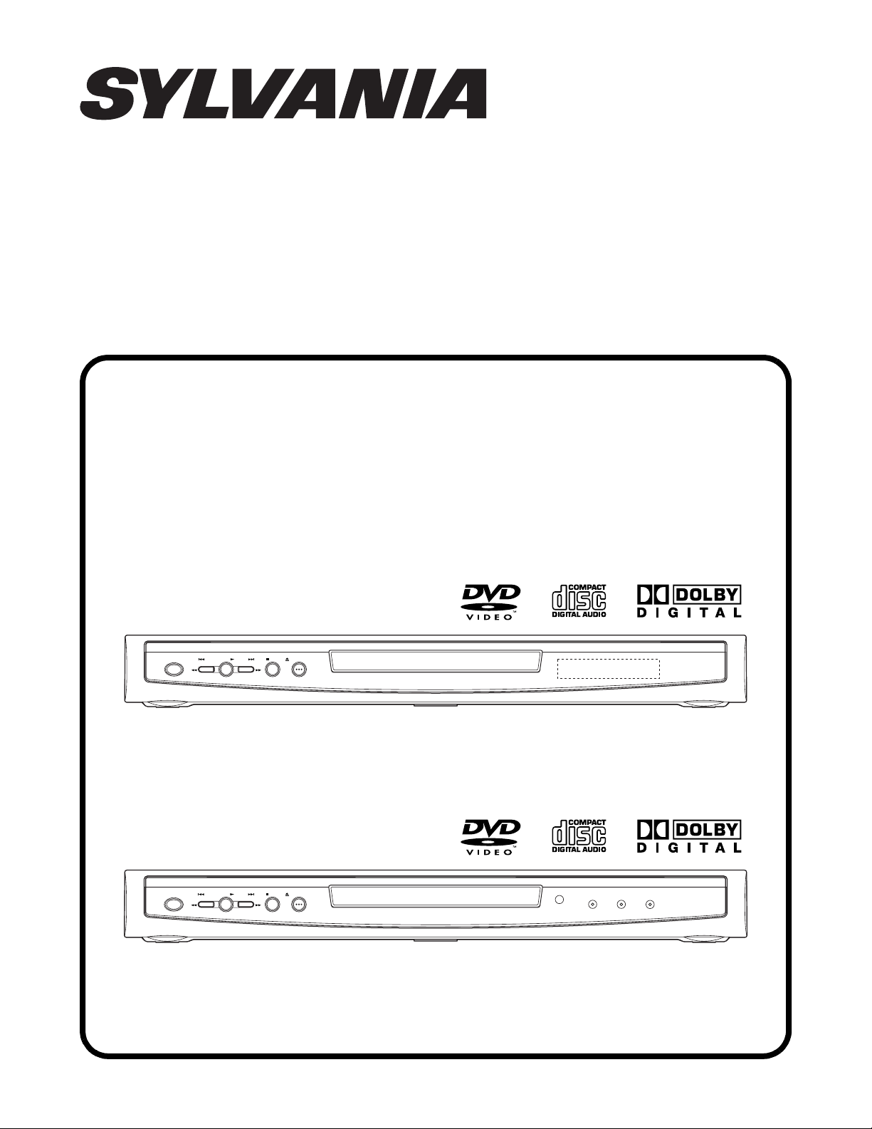
SERVICE MANUAL
DVD PLAYER
DVL700F
POWER SKIP SKIPPLAY STOP OPEN/CLOSE
POWER SKIP SKIPPLAY STOP OPEN/CLOSE
DVL150F
POWER
PLAY
PROGRESSIVE SCAN
Page 2

IMPORTANT SAFETY NOTICE
Proper service and repair is important to the safe, reliable operation of all
Funai Equipment. The service procedures recommended by Funai and
described in this service manual are effective methods of performing
service operations. Some of these service special tools should be used
when and as recommended.
It is important to note that this service manual contains various CAUTIONS
and NOTICES which should be carefully read in order to minimize the risk
of personal injury to service personnel. The possibility exists that improper
service methods may damage the equipment. It also is important to
understand that these CAUTIONS and NOTICES ARE NOT EXHAUSTIVE.
Funai could not possibly know, evaluate and advice the service trade of all
conceivable ways in which service might be done or of the possible
hazardous consequences of each way. Consequently, Funai has not
undertaken any such broad evaluation. Accordingly, a servicer who uses a
service procedure or tool which is not recommended by Funai must first
use all precautions thoroughly so that neither his safety nor the safe
operation of the equipment will be jeopardized by the service method
selected.
TABLE OF CONTENTS
Specifications . . . . . . . . . . . . . . . . . . . . . . . . . . . . . . . . . . . . . . . . . . . . . . . . . . . . . . . . . . . . . . . . . . . . . . . . . . 1-1-1
Laser Beam Safety Precautions . . . . . . . . . . . . . . . . . . . . . . . . . . . . . . . . . . . . . . . . . . . . . . . . . . . . . . . . . . . . 1-2-1
Important Safety Precautions . . . . . . . . . . . . . . . . . . . . . . . . . . . . . . . . . . . . . . . . . . . . . . . . . . . . . . . . . . . . . . 1-3-1
Standard Notes for Servicing . . . . . . . . . . . . . . . . . . . . . . . . . . . . . . . . . . . . . . . . . . . . . . . . . . . . . . . . . . . . . . 1-4-1
Cabinet Disassembly Instructions. . . . . . . . . . . . . . . . . . . . . . . . . . . . . . . . . . . . . . . . . . . . . . . . . . . . . . . . . . .1-5-1
How to Initialize the DVD Player . . . . . . . . . . . . . . . . . . . . . . . . . . . . . . . . . . . . . . . . . . . . . . . . . . . . . . . . . . . . 1-6-1
Firmware Renewal Mode . . . . . . . . . . . . . . . . . . . . . . . . . . . . . . . . . . . . . . . . . . . . . . . . . . . . . . . . . . . . . . . . . 1-7-1
Block Diagrams . . . . . . . . . . . . . . . . . . . . . . . . . . . . . . . . . . . . . . . . . . . . . . . . . . . . . . . . . . . . . . . . . . . . . . . . . 1-8-1
Schematic Diagrams / CBA’s and Test Points. . . . . . . . . . . . . . . . . . . . . . . . . . . . . . . . . . . . . . . . . . . . . . . . . . 1-9-1
Waveforms . . . . . . . . . . . . . . . . . . . . . . . . . . . . . . . . . . . . . . . . . . . . . . . . . . . . . . . . . . . . . . . . . . . . . . . . . . .1-10-1
Wiring Diagram . . . . . . . . . . . . . . . . . . . . . . . . . . . . . . . . . . . . . . . . . . . . . . . . . . . . . . . . . . . . . . . . . . . . . . . . 1-11-1
System Control Timing Charts . . . . . . . . . . . . . . . . . . . . . . . . . . . . . . . . . . . . . . . . . . . . . . . . . . . . . . . . . . . . 1-12-1
IC Pin Function Descriptions. . . . . . . . . . . . . . . . . . . . . . . . . . . . . . . . . . . . . . . . . . . . . . . . . . . . . . . . . . . . . . 1-13-1
Lead Identifications . . . . . . . . . . . . . . . . . . . . . . . . . . . . . . . . . . . . . . . . . . . . . . . . . . . . . . . . . . . . . . . . . . . . . 1-14-1
Exploded Views. . . . . . . . . . . . . . . . . . . . . . . . . . . . . . . . . . . . . . . . . . . . . . . . . . . . . . . . . . . . . . . . . . . . . . . . 1-15-1
Mechanical Parts List . . . . . . . . . . . . . . . . . . . . . . . . . . . . . . . . . . . . . . . . . . . . . . . . . . . . . . . . . . . . . . . . . . .1-16-1
Electrical Parts List . . . . . . . . . . . . . . . . . . . . . . . . . . . . . . . . . . . . . . . . . . . . . . . . . . . . . . . . . . . . . . . . . . . . . 1-17-1
Manufactured under license from Dolby Laboratories.
“Dolby” and the double-D symbol are trademarks of Dolby Laboratories.
Page 3
SPECIFICATIONS
Item Conditions Unit Nominal Limit
1. Video Output 75 Ω load Vpp 1.0 ± 0.1
2. Coaxial Digital Out 75 Ω load mVpp 500 ± 50
3. Audio (PCM)
3-1. Output Level 1 kHz, 0 dB, 47k Ω load Vrms 2.0
3-2. S/N 47k Ω load dB 120
3-3. Freq. Response
DVD fs = 48 kHz ± 0.5 dB, 47k Ω load Hz 20 ~ 22 k
CD fs = 44.1 kHz ± 0.5 dB, 47k Ω load Hz 20 ~ 20 k
3-4. THD+N
DVD 1 kHz, 0 dB, 47k Ω load % 0.0035
CD 1 kHz, 0 dB, 47k Ω load % 0.004
Notes:
1. All Items are measured without pre-emphasis unless otherwise specified.
2. Power supply: AC 120 V, 60 Hz
3. Ambient Temperature: +25 °C
1-1-1 E6161SP
Page 4
LASER BEAM SAFETY PRECAUTIONS
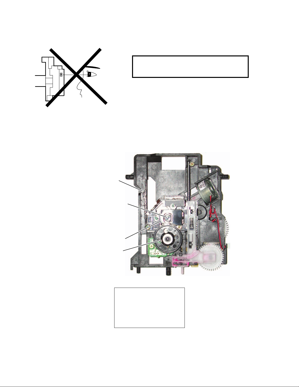
This DVD player uses a pickup that emits a laser beam.
Do not look directly at the laser beam coming
from the pickup or allow it to strike against your
skin.
The laser beam is emitted from the location shown in the figure. When checking the laser diode, be sure to keep
your eyes at least 30 cm away from the pickup lens when the diode is turned on. Do not look directly at the laser
beam.
CAUTION: Use of controls and adjustments, or doing procedures other than those specified herein, may result in
hazardous radiation exposure.
Drive Mechanism
Assembly
Laser Beam Radiation
Laser Pickup
Turntable
LASER RADIATION
WHEN OPEN. DO NOT
CAUTION
STARE INTO BEAM.
Location: Top of DVD mechanism.
1-2-1 E6NLSP
Page 5

IMPORTANT SAFETY PRECAUTIONS
Product Safety Notice
Some electrical and mechanical parts have special
safety-related characteristics which are often not
evident from visual inspection, nor can the protection
they give necessarily be obtained by replacing them
with components rated for higher voltage, wattage,
etc. Parts that have special safety characteristics are
identified by a # on schematics and in parts lists. Use
of a substitute replacement that does not have the
same safety characteristics as the recommended
replacement part might create shock, fire, and/or other
hazards. The Product’s Safety is under review
continuously and new instructions are issued
whenever appropriate. Prior to shipment from the
factory, our products are carefully inspected to confirm
with the recognized product safety and electrical
codes of the countries in which they are to be sold.
However, in order to maintain such compliance, it is
equally important to implement the following
precautions when a set is being serviced.
Precautions during Servicing
A. Parts identified by the # symbol are critical for
safety. Replace only with part number specified.
B. In addition to safety, other parts and assemblies
are specified for conformance with regulations
applying to spurious radiation. These must also be
replaced only with specified replacements.
Examples: RF converters, RF cables, noise
blocking capacitors, and noise blocking filters, etc.
C. Use specified internal wiring. Note especially:
1) Wires covered with PVC tubing
2) Double insulated wires
3) High voltage leads
D. Use specified insulating materials for hazardous
live parts. Note especially:
1) Insulation tape
2) PVC tubing
3) Spacers
4) Insulators for transistors
E. When replacing AC primary side components
(transformers, power cord, etc.), wrap ends of
wires securely about the terminals before
soldering.
F. Observe that the wires do not contact heat
producing parts (heat sinks, oxide metal film
resistors, fusible resistors, etc.).
G. Check that replaced wires do not contact sharp
edges or pointed parts.
H. When a power cord has been replaced, check that
5 - 6 kg of force in any direction will not loosen it.
I. Also check areas surrounding repaired locations.
J. Be careful that foreign objects (screws, solder
droplets, etc.) do not remain inside the set.
K. Crimp type wire connector
The power transformer uses crimp type
connectors which connect the power cord and the
primary side of the transformer. When replacing
the transformer, follow these steps carefully and
precisely to prevent shock hazards.
Replacement procedure
1) Remove the old connector by cutting the wires
at a point close to the connector.
Important: Do not re-use a connector.
(Discard it.)
2) Strip about 15 mm of the insulation from the
ends of the wires. If the wires are stranded,
twist the strands to avoid frayed conductors.
3) Align the lengths of the wires to be connected.
Insert the wires fully into the connector.
4) Use a crimping tool to crimp the metal sleeve at
its center. Be sure to crimp fully to the complete
closure of the tool.
L. When connecting or disconnecting the internal
connectors, first, disconnect the AC plug from the
AC outlet.
1-3-1 DVDN_ISP
Page 6
Safety Check after Servicing
Examine the area surrounding the repaired location for damage or deterioration. Observe that screws, parts, and
wires have been returned to their original positions. Afterwards, do the following tests and confirm the specified
values to verify compliance with safety standards.
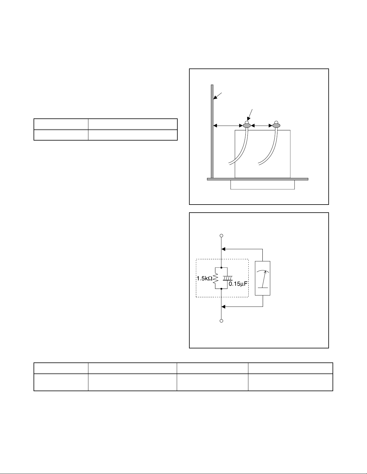
1. Clearance Distance
When replacing primary circuit components, confirm
specified clearance distance (d) and (d’) between
soldered terminals, and between terminals and
surrounding metallic parts. (See Fig. 1)
Table 1: Ratings for selected area
Chassis or Secondary Conductor
Primary Circuit Terminals
AC Line Voltage Clearance Distance (d), (d’)
120 V ≥ 3.2 mm (0.126 inches)
Note: This table is unofficial and for reference only. Be
sure to confirm the precise values.
2. Leakage Current Test
Confirm the specified (or lower) leakage current
between B (earth ground, power cord plug prongs) and
externally exposed accessible parts (RF terminals,
antenna terminals, video and audio input and output
terminals, microphone jacks, earphone jacks, etc.) is
lower than or equal to the specified value in the table
below.
Measuring Method (Power ON):
Insert load Z between B (earth ground, power cord plug
prongs) and exposed accessible parts. Use an AC
voltmeter to measure across the terminals of load Z.
See Fig. 2 and the following table.
dd'
Fig. 1
Exposed Accessible Part
Z
AC Voltmeter
(High Impedance)
Earth Ground
B
Power Cord Plug Prongs
Table 2: Leakage current ratings for selected areas
AC Line Voltage Load Z Leakage Current (i) Earth Ground (B) to:
120 V
Note: This table is unofficial and for reference only. Be sure to confirm the precise values.
0.15 µF CAP. & 1.5 kΩ RES.
Connected in parallel
i ≤ 0.5 mA Peak Exposed accessible parts
1-3-2 DVDN_ISP
Fig. 2
Page 7
STANDARD NOTES FOR SERVICING
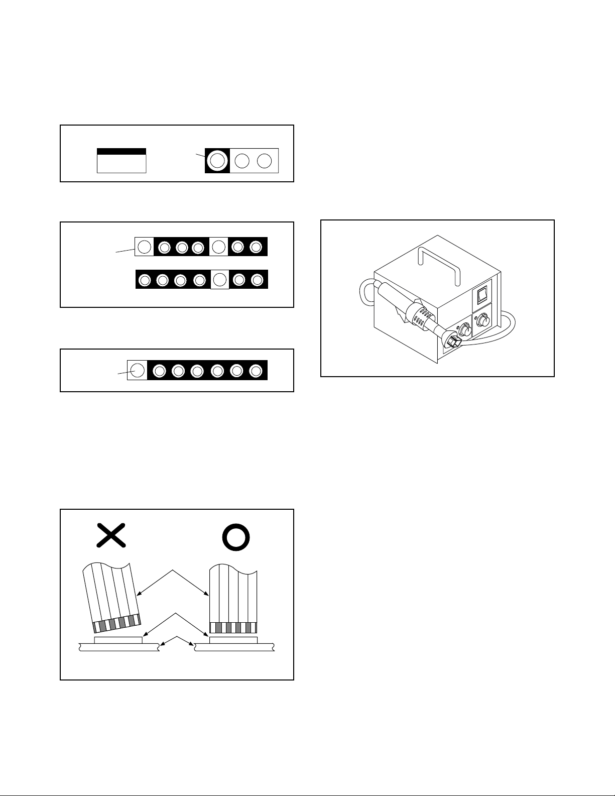
Circuit Board Indications
1. The output pin of the 3 pin Regulator ICs is
indicated as shown.
Top View
Out
2. For other ICs, pin 1 and every fifth pin are
indicated as shown.
Pin 1
3. The 1st pin of every male connector is indicated as
shown.
Pin 1
Input
In
Bottom View
5
10
Pb (Lead) Free Solder
When soldering, be sure to use the Pb free solder.
How to Remove / Install Flat Pack-IC
1. Removal
With Hot-Air Flat Pack-IC Desoldering Machine:
1. Prepare the hot-air flat pack-IC desoldering
machine, then apply hot air to the Flat Pack-IC
(about 5 to 6 seconds). (Fig. S-1-1)
Fig. S-1-1
Instructions for Connectors
1. When you connect or disconnect the FFC (Flexible
Foil Connector) cable, be sure to first disconnect
the AC cord.
2. FFC (Flexible Foil Connector) cable should be
inserted parallel into the connector, not at an
angle.
FFC Cable
Connector
CBA
* Be careful to avoid a short circuit.
2. Remove the flat pack-IC with tweezers while
applying the hot air.
3. Bottom of the flat pack-IC is fixed with glue to the
CBA; when removing entire flat pack-IC, first apply
soldering iron to center of the flat pack-IC and heat
up. Then remove (glue will be melted). (Fig. S-1-6)
4. Release the flat pack-IC from the CBA using
tweezers. (Fig. S-1-6)
CAUTION:
1. The Flat Pack-IC shape may differ by models. Use
an appropriate hot-air flat pack-IC desoldering
machine, whose shape matches that of the Flat
Pack-IC.
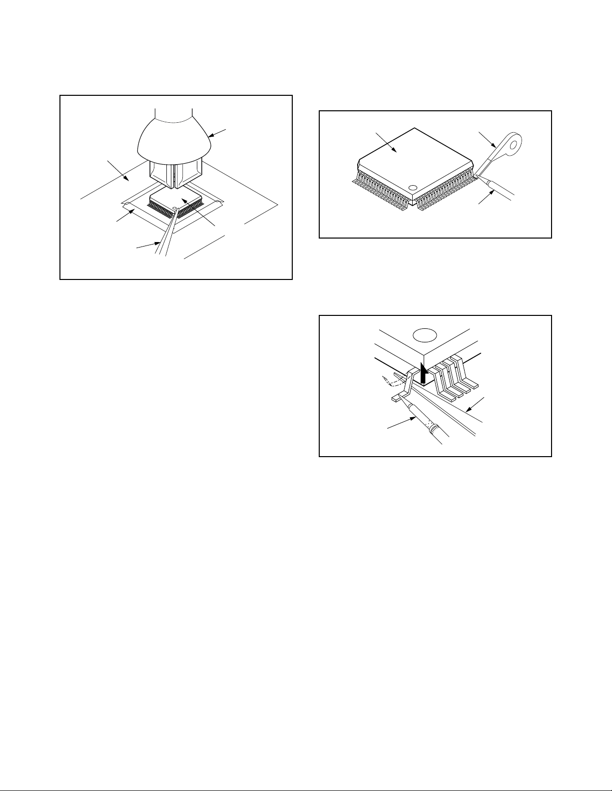
2. Do not supply hot air to the chip parts around the
flat pack-IC for over 6 seconds because damage
to the chip parts may occur. Put masking tape
around the flat pack-IC to protect other parts from
damage. (Fig. S-1-2)
1-4-1 DVDN_SN
Page 8
3. The flat pack-IC on the CBA is affixed with glue, so
be careful not to break or damage the foil of each
pin or the solder lands under the IC when
removing it.
With Soldering Iron:
1. Using desoldering braid, remove the solder from
all pins of the flat pack-IC. When you use solder
flux which is applied to all pins of the flat pack-IC,
you can remove it easily. (Fig. S-1-3)
CBA
Masking
Tape
Tweezers
Hot-air
Flat Pack-IC
Desoldering
Machine
Flat Pack-IC
Fig. S-1-2
Flat Pack-IC
Desoldering Braid
Soldering Iron
Fig. S-1-3
2. Lift each lead of the flat pack-IC upward one by
one, using a sharp pin or wire to which solder will
not adhere (iron wire). When heating the pins, use
a fine tip soldering iron or a hot air desoldering
machine. (Fig. S-1-4)
Sharp
Pin
Fine Tip
Soldering Iron
3. Bottom of the flat pack-IC is fixed with glue to the
CBA; when removing entire flat pack-IC, first apply
soldering iron to center of the flat pack-IC and heat
up. Then remove (glue will be melted). (Fig. S-1-6)
4. Release the flat pack-IC from the CBA using
tweezers. (Fig. S-1-6)
Fig. S-1-4
1-4-2 DVDN_SN
Page 9
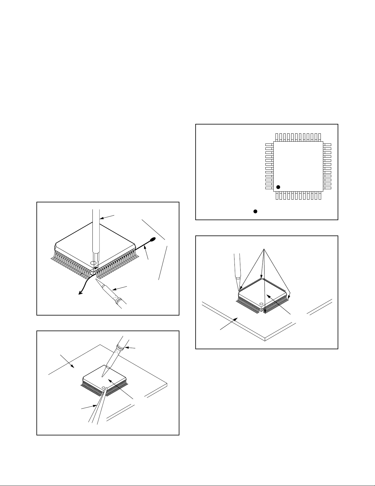
With Iron Wire:
1. Using desoldering braid, remove the solder from
all pins of the flat pack-IC. When you use solder
flux which is applied to all pins of the flat pack-IC,
you can remove it easily. (Fig. S-1-3)
2. Affix the wire to a workbench or solid mounting
point, as shown in Fig. S-1-5.
3. While heating the pins using a fine tip soldering
iron or hot air blower, pull up the wire as the solder
melts so as to lift the IC leads from the CBA
contact pads as shown in Fig. S-1-5.
4. Bottom of the flat pack-IC is fixed with glue to the
CBA; when removing entire flat pack-IC, first apply
soldering iron to center of the flat pack-IC and heat
up. Then remove (glue will be melted). (Fig. S-1-6)
5. Release the flat pack-IC from the CBA using
tweezers. (Fig. S-1-6)
Note: When using a soldering iron, care must be
taken to ensure that the flat pack-IC is not
being held by glue. When the flat pack-IC is
removed from the CBA, handle it gently
because it may be damaged if force is applied.
Hot Air Blower
2. Installation
1. Using desoldering braid, remove the solder from
the foil of each pin of the flat pack-IC on the CBA
so you can install a replacement flat pack-IC more
easily.
2. The “●” mark on the flat pack-IC indicates pin 1.
(See Fig. S-1-7.) Be sure this mark matches the 1
on the PCB when positioning for installation. Then
presolder the four corners of the flat pack-IC. (See
Fig. S-1-8.)
3. Solder all pins of the flat pack-IC. Be sure that
none of the pins have solder bridges.
Example :
Pin 1 of the Flat Pack-IC
is indicated by a " " mark.
Fig. S-1-7
To Solid
Mounting Point
CBA
Tweezers
Iron Wire
Soldering Iron
Fig. S-1-5
Fine Tip
Soldering Iron
Flat Pack-IC
or
Presolder
Flat Pack-IC
CBA
Fig. S-1-8
Fig. S-1-6
1-4-3 DVDN_SN
Page 10
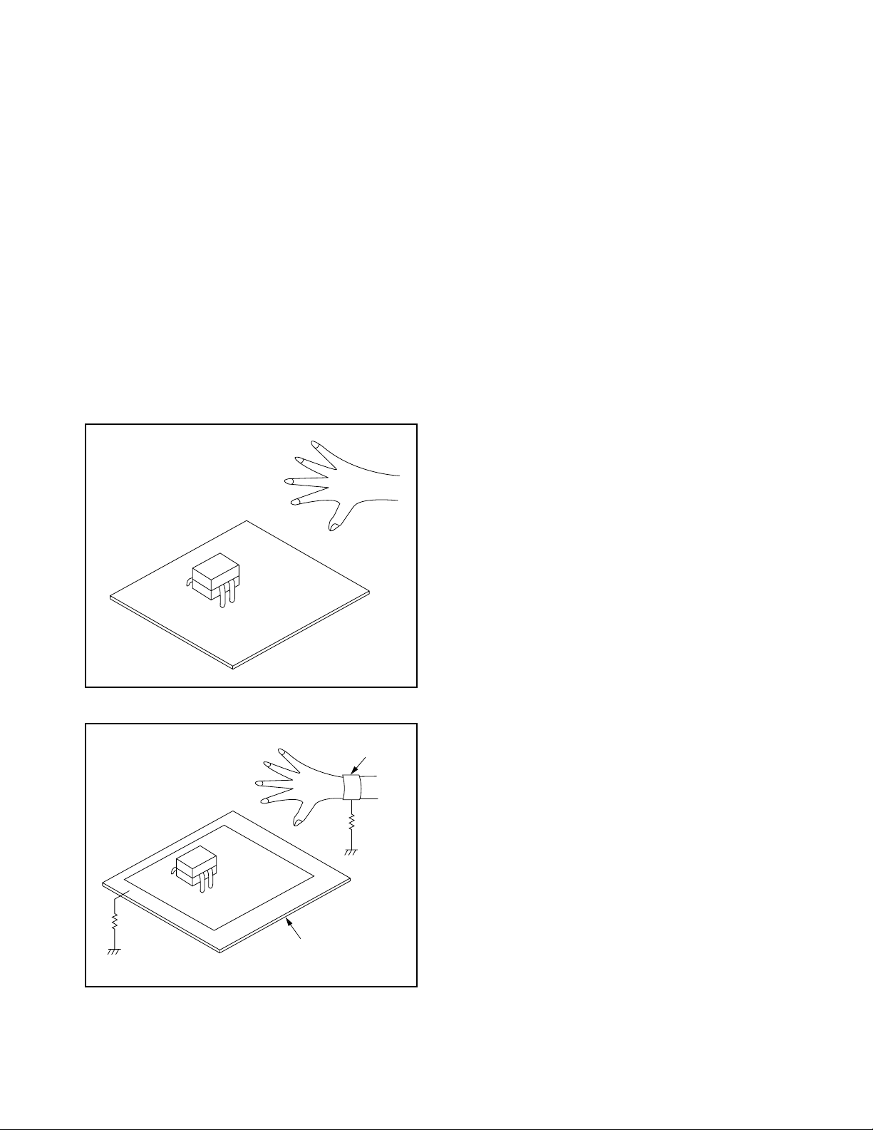
Instructions for Handling Semiconductors
Electrostatic breakdown of the semi-conductors may
occur due to a potential difference caused by
electrostatic charge during unpacking or repair work.
1. Ground for Human Body
Be sure to wear a grounding band (1 MΩ) that is
properly grounded to remove any static electricity that
may be charged on the body.
2. Ground for Workbench
Be sure to place a conductive sheet or copper plate
with proper grounding (1 MΩ) on the workbench or
other surface, where the semi-conductors are to be
placed. Because the static electricity charge on
clothing will not escape through the body grounding
band, be careful to avoid contacting semi-conductors
with your clothing.
<Incorrect>
<Correct>
1MΩ
CBA
Grounding Band
1MΩ
CBA
Conductive Sheet or
Copper Plate
1-4-4 DVDN_SN
Page 11
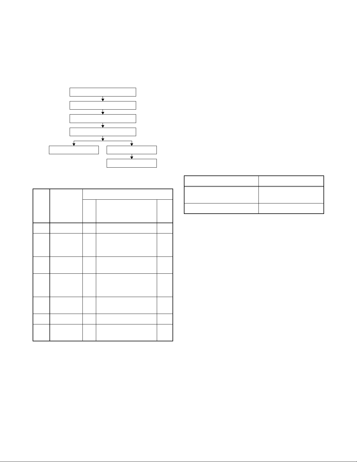
CABINET DISASSEMBLY INSTRUCTIONS
1. Disassembly Flowchart
This flowchart indicates the disassembly steps to gain
access to item(s) to be serviced. When reassembling,
follow the steps in reverse order. Bend, route, and
dress the cables as they were originally.
[1] Top Case
[2] Front Assembly
[3] Reinforce Plate
[4] DVD Main CBA Unit
[5] DVD Mechanism [6] AV CBA
[7] Function CBA
2. Disassembly Method
ID/
Loc.
No.
[1] Top Case D1 3(S-1) -
[2]
[3]
[4]
[5]
[6] AV CBA D6 (S-5), 4(S-6), *2(L-5) -
[7]
↓
(1)
Part
Front
Assembly
Reinforce
Plate
DVD Main
CBA Unit
DVD
MechanismD4D5
Function
CBA
↓
(2)
Fig.
No.
D2
D3 2(S-2) -
D4
D6 *CN2001 -
↓
(3)
*2(L-1), Tray Panel,
*4(L-2), *3(L-3),
*3(L-4)
(S-3A), (S-3B),
*CN201, *CN301,
*CN401, *CN601
4(S-4)
Removal
Remove/*Unhook/
Unlock/Release/
Unplug/Desolder
↓
(4)
Note
1
2
2
3
↓
(5)
Note:
(1) Identification (location) No. of parts in the figures
(2) Name of the part
(3) Figure Number for reference
(4) Identification of parts to be removed, unhooked,
unlocked, released, unplugged, unclamped, or
desoldered.
P = Spring, L = Locking Tab, S = Screw,
CN = Connector
* = Unhook, Unlock, Release, Unplug, or Desolder
e.g. 2(S-2) = two Screws (S-2),
2(L-2) = two Locking Tabs (L-2)
(5) Refer to “Reference Notes.”
About tightening screws
When tightening screws, tighten them with the
following torque.
Screws Torque
(S-1), (S-2), (S-3A), (S-4),
(S-5), (S-6)
(S-3B) 0.38 ± 0.04 N·m
0.45 ± 0.05 N·m
Reference Notes
1. CAUTION 1: Locking Tabs (L-1), (L-2), (L-3) and
(L-4) are fragile. Be careful not to break them.
1) Connect the wall plug to an AC outlet and press
the [A OPEN/CLOSE] button to open the tray.
2) Remove the Tray Panel by releasing two
locking tabs (L-1).
3) Press the [A OPEN/CLOSE] button again to
close the tray.
4) Press the [POWER] button to turn the power
off.
5) Unplug an AC cord.
6) Release four Locking Tabs (L-2), then release
three Locking Tabs (L-3).
7) Release three Locking Tabs (L-4), and remove
the Front Assembly.
2. CAUTION 2: Electrostatic breakdown of the laser
diode in the optical system block may occur as a
potential difference caused by electrostatic charge
accumulated on cloth, human body etc, during
unpacking or repair work.
To avoid damage of pickup follow next procedures.
1) Short the three short lands of FPC cable with
solder before removing the FFC cable (CN201)
from it. If you disconnect the FFC cable
(CN201), the laser diode of pickup will be
destroyed. (Fig. D4)
1-5-1 E6121DC
Page 12
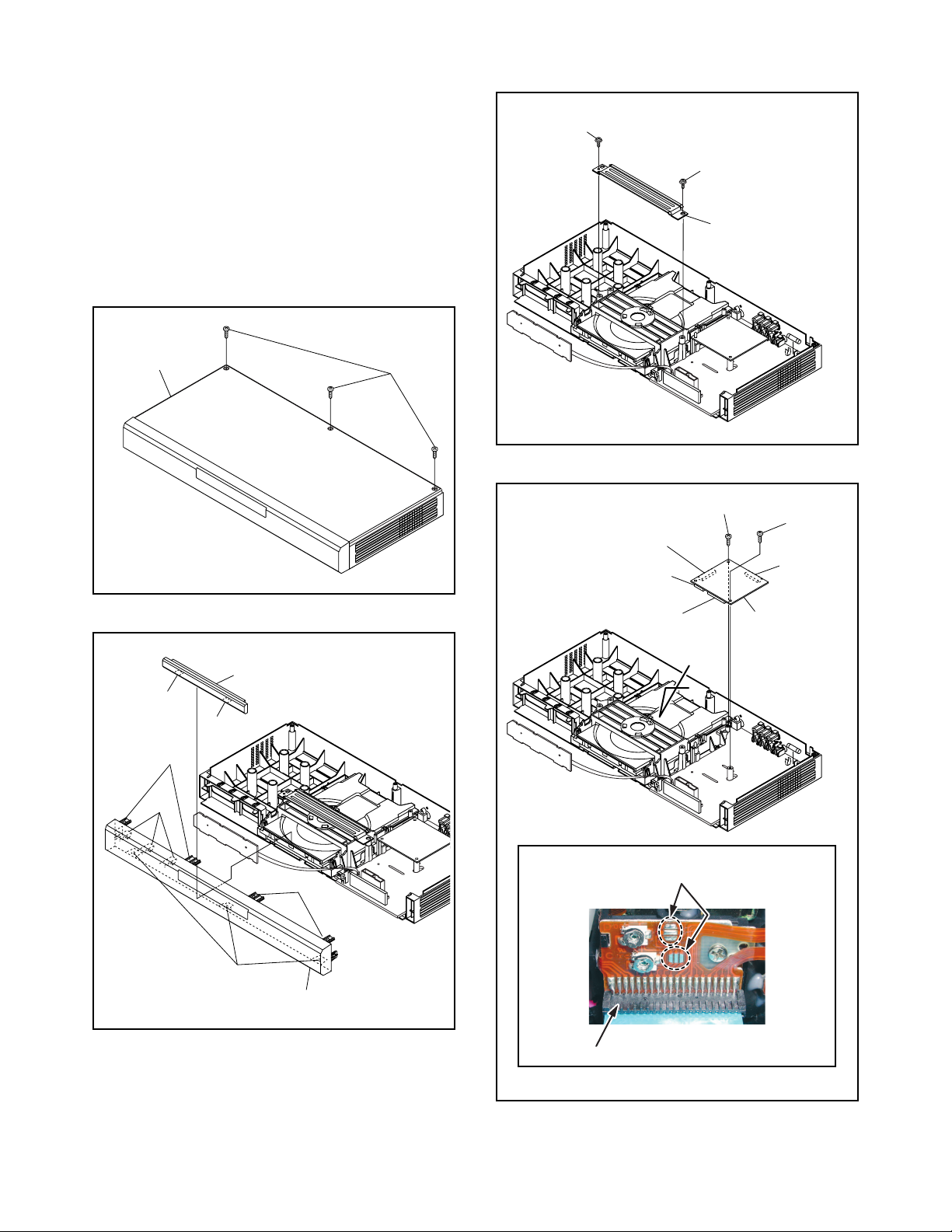
2) Disconnect Connectors (CN301), (CN401) and
(CN601). Remove two Screws (S-3A) and
(S-3B) and lift the DVD Main CBA Unit.
(Fig. D4)
3. CAUTION 3: When reassembling, confirm the
FFC cable (CN201) is connected completely. Then
remove the solder from the three short lands of
FPC cable. (Fig. D4)
Note: The illustrations used in the following
procedures are of the model DVL700F which
is VFD model.
(S-2)
(S-2)
[3] Reinforce Plate
[1] Top Case
(L-1)
(L-2)
(L-4)
(L-1)
Tray Panel
(S-1)
Fig. D1
CN201
CN301
CN401
Fig. D3
(S-3B)
(S-3A)
CN601
[4] DVD Main
CBA Unit
A
(L-2)
(L-3)
[2] Front Assembly
Fig. D2
Short the three short lands by soldering.
(Either of two places.)
Connector
View for A
Fig. D4
1-5-2 E6121DC
Page 13
(S-4)
[5] DVD Mechanism
(S-4)
(S-4)
[7] Function CBA
(S-5)
CN2001
[6] AV CBA
(S-6)
(L-5)
Fig. D5
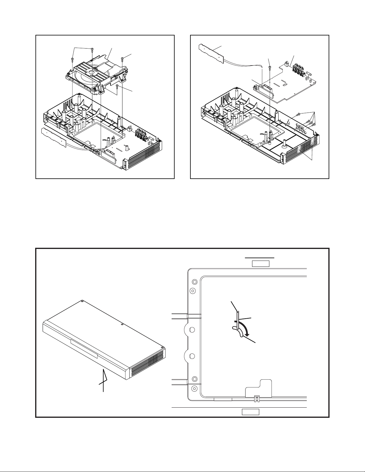
3. How to Eject Manually
1. Turn the unit over.
2. Insert the shaft less than a diameter of 3 mm (e.g. screwdriver) straightly into the opening as shown.
3. Turn the shaft along with the opening clockwise.
4. Repeat steps 2 and 3 until the tray will open.
5. Pull the tray slowly with a hand.
View for B
Rear
Turn the shaft along with
the opening clockwise.
Shaft
(e.g. screwdriver)
Opening
Fig. D6
B
Front
1-5-3 E6121DC
Page 14

HOW TO INITIALIZE THE DVD PLAYER
To put the program back at the factory-default,
initialize the DVD player as the following procedure.
1. Press [1], [2], [3], [4], and [DISPLAY] buttons on
the remote control unit in that order.
Fig. a appears on the screen.
"
" differ depending on the models.
*******
MODEL : *******
Version
Region
: *.**
: *
EXIT: POWEREEPROM CLEAR : CLEAR
Fig. a
"
" differ depending on the models.
*******
2. Press [CLEAR] button on the remote control unit.
Fig. b appears on the screen.
MODEL : *******
Version
Region
: *.**
: *
EXIT: POWEREEPROM CLEAR : CLEAR
EEPROM CLEAR : OK
Fig. b
When “OK” appears on the screen, the factory
default will be set. Then the firmware renewal
mode is complete.
3. To exit this mode, press [POWER] button.
1-6-1 E6121INT
Page 15
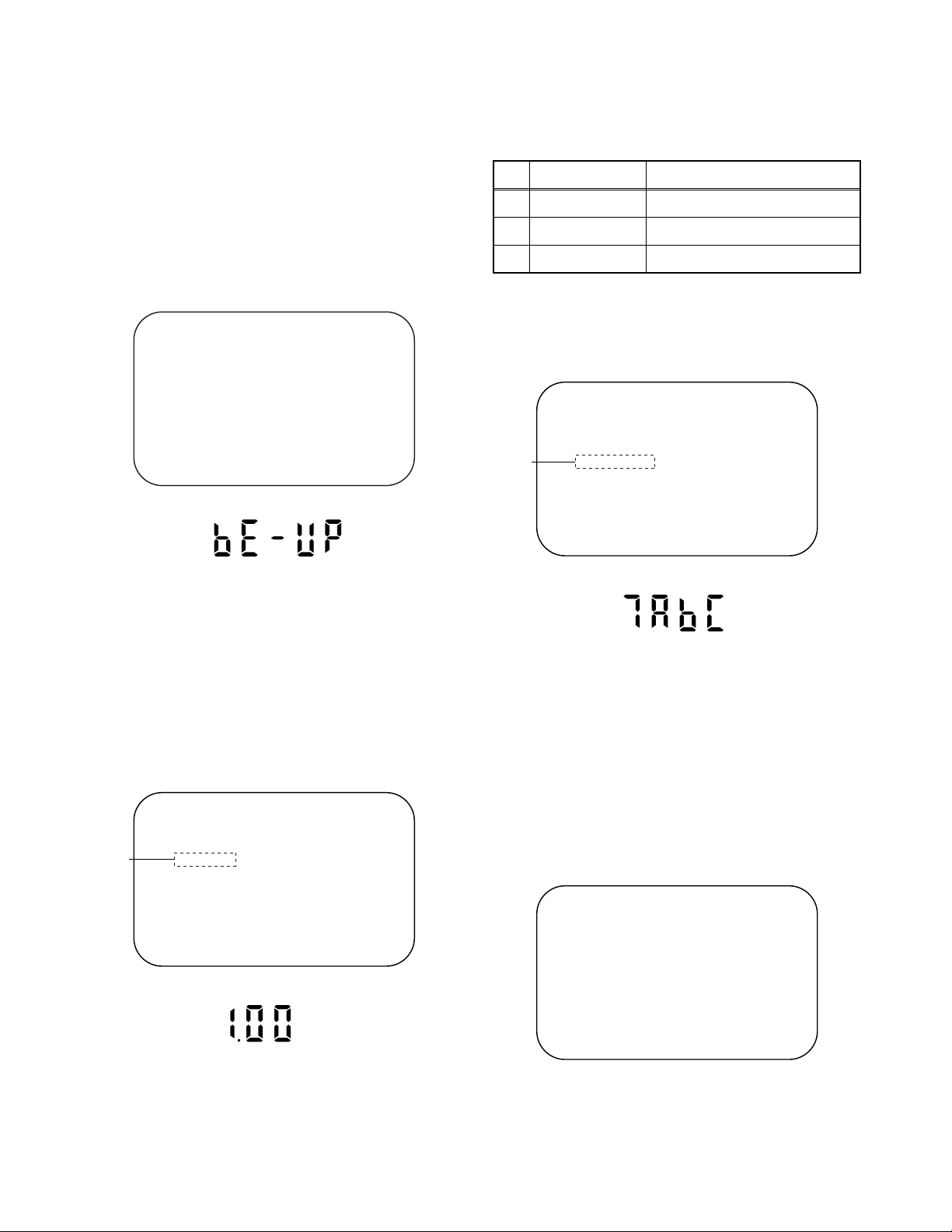
FIRMWARE RENEWAL MODE
Note: The VFD indication only appears in the model
DVL700F.
1. Turn the power on and remove the disc on the tray.
2. To put the DVD player into version up mode, press
[9], [8], [7], [6], and [SEARCH MODE] buttons on
the remote control unit in that order. The tray will
open automatically.
Fig. a appears on the screen and Fig. b appears
on the VFD.
"
" differ depending on the models.
*******
F/W Version Up Mode Model No : *******
Please insert a DISC
for F/W Version Up.
Fig. a Version Up Mode Screen
Fig. b VFD in Version Up Mode
VERSION : *.**
EXIT: POWER
The appearance shown in (*1) of Fig. c is
described as follows:
No. Appearance State
1 Reading... Sending files into the memory
2 Erasing... Erasing previous version data
3 Programming... Writing new version data
5. After programming is finished, the tray opens
automatically. Fig. e appears on the screen and
the checksum in (*2) of Fig. e appears on the VFD
(Fig. f).
"
" differ depending on the models.
*******
F/W Version Up Mode
VERSION : ************.ab6
Completed
(*2)
SUM : 7ABC
Fig. e Completed Program Mode Screen
Model No : *******
VERSION : *.**
The DVD player can also enter the version up
mode with the tray open. In this case, Fig. a will be
shown on the screen while the tray is open.
3. Load the disc for version up.
4. The DVD player enters the F/W version up mode
automatically. Fig. c appears on the screen and
Fig. d appears on the VFD. If you enter the F/W for
different models, “Disc Error” will appear on the
screen, then the tray will open automatically.
"
" differ depending on the models.
*******
F/W Version Up Mode Model No : *******
VERSION : ************.ab6
(*1)
Reading...
Fig. c Programming Mode Screen
Fig. d VFD in Programming Mode (Example)
VERSION : *.**
Fig. f VFD upon Finishing the Programming Mode (Example)
At this time, no buttons are available.
6. Remove the disc on the tray.
7. Unplug the AC cord from the AC outlet. Then plug
it again.
8. Turn the power on by pressing the [POWER]
button and the tray will close.
9. Press [1], [2], [3], [4], and [DISPLAY] buttons on
the remote control unit in that order.
Fig. g appears on the screen.
"
" differ depending on the models.
*******
MODEL : *******
Version
Region
: *.**
: *
EXIT: POWEREEPROM CLEAR : CLEAR
Fig. g
1-7-1 E6121FW
Page 16

10. Press [CLEAR] button on the remote control unit.
Fig. h appears on the screen.
"
" differ depending on the models.
*******
MODEL : *******
Version
Region
: *.**
: *
EXIT: POWEREEPROM CLEAR : CLEAR
EEPROM CLEAR : OK
Fig. h
When “OK” appears on the screen, the factory
default will be set. Then the firmware renewal
mode is complete.
11. To exit this mode, press [POWER] button.
1-7-2 E6121FW
Page 17
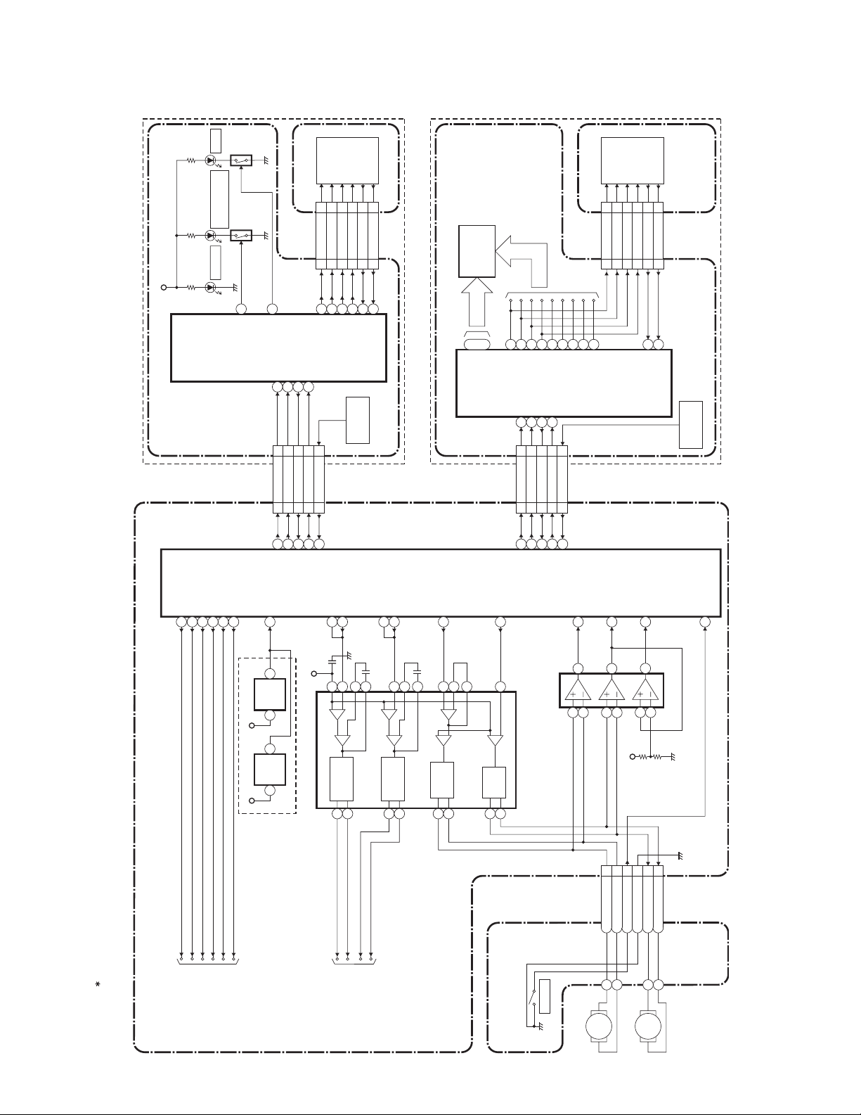
BLOCK DIAGRAMS
System Control / Servo Block Diagram
D2022
PLAY
Q2022
KEY
MATRIX
KEY
MATRIX
DVL150F
IC101
(MICRO CONTROLLER)
+5V
IC2001
(FRONT PANEL CONTROL)
PCM-SCLK
I/P-SW
163
183
D2021
PROGRESSIVE
SCAN
D2023
POWER
ADAC-MD
AUDIO-MUTE
57
56 ADAC-MC
88
Q2021
19
PROGRESSIVE
SCAN-LED
86 ADAC-ML
18
PLAY-LED
FP-STB
FP-DIN
2
28
CN1001
FP-STB 23
FP-DIN 22
2120221923
CN401
82
60
FP-DIN
FP-STB
RESET73
CN2001 CN2101
FP-DOUT
FP-CLK
1
27
FP-DOUT 24
FP-CLK 21
REMOTE 25
61
67
59
FP-CLK
REMOTE
FP-DOUT
KEY-1 5
KEY-2 3
5
3
789
KEY-1
KEY-2
FD-OFST
146
KEY-3 4
K2 1
KEY-4 6
K1 2
4
1
6
2
3
4
10
K1
K2
KEY-3
KEY-4
SENSOR
REMOTE
RM2001
FOCUS DRIVE
148
FUNCTION CBA
AV CBA
TRACKING
DRIVE
TD-OFST
147
139
DVL700F
FL2001
IC2001
(FRONT PANEL CONTROL)
SPDL
76
FUNCTION CBA
KEY-1 5
KEY-3 4
K2 1
KEY-2 3
KEY-4 6
5
SEGMENT
GRID FIP
~
789
a/KEY-1
CN1001
CN401
SLD75
10
c/KEY-3
b/KEY-2
d/KEY-4
FP-STB
FP-DIN
FP-DOUT
2
28
27
FP-STB 23
FP-DIN 22
FP-DOUT 24
2120221923
82
60
61
FP-DIN
FP-STB
FP-DOUT
23
17
~
7G
1G
12
11
f
e
FP-CLK
1
FP-CLK 21
REMOTE 25
67
59
FP-CLK
REMOTE
131416
g
h
SP-ROT
143
CN2001 CN2101
i
SL-ADS
140
K1 2
4
1
3
6
2
3
4
K1
K2
AV CBA
SENSOR
REMOTE
RM2001
SL-AMP
81
TRAY-IN
66
VREF
RESET
IC462
1 3
+3.3V
RESET
IC461
2 1
(SERVO DRIVE)
+3.3V
*1
I/P-SW
1 NOTE:
Either IC461 or IC462 is used for DVD MAIN CBA UNIT.
AUDIO-MUTE
ADAC-MD
PCM-SCLK
TO
VIDEO/ AUDIO
BLOCK DIAGRAM
ADAC-MC
ADAC-ML
IC301
26
27
-
+
+
FOCUS
ACTUATOR
15
FS(+)
FS(-)
-
DRIVE
16
TO DIGITAL SIGNAL
24
25
-
+
-
+
TRACKING
ACTUATOR
14
TS(+)
TS(-)
PROCESS BLOCK
DIAGRAM
DRIVE
13
312
-
+
-
+
SPINDLE
MOTOR
DRIVE
12
11
1
7
14
645
23
IC202
+
SLED
MOTOR
17
-
DRIVE
18
(OP AMP)
3
6
2
5
3SP(+)
CN301
4SP(-)
12
+3.3V
5TRAY-IN
6GND
13
7SL(-)
DVD MAIN CBA UNIT
8SL(+)
DRIVE CBA
TRAY-IN
SPINDLE
MOTOR
M
SLED
MOTOR
M
1-8-1
E6121BLS
Page 18
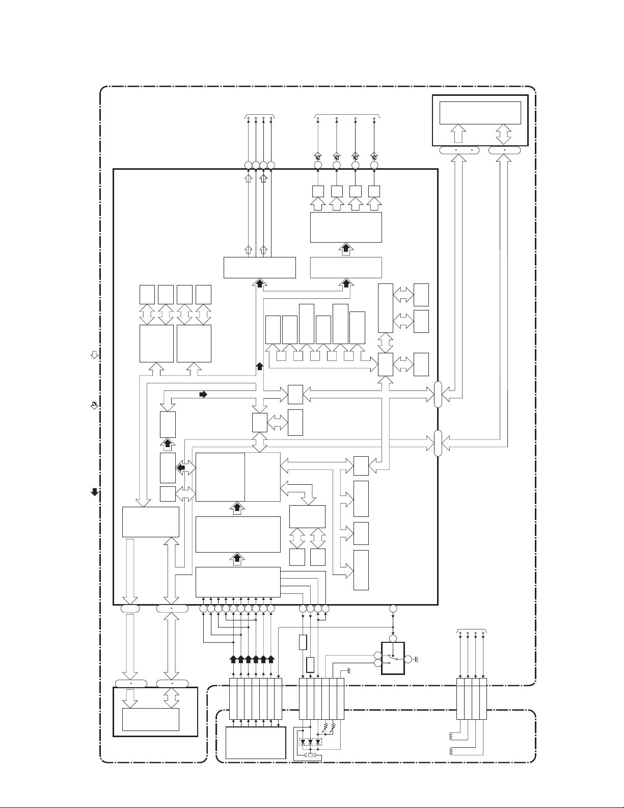
Digital Signal Process Block Diagram
TO
VIDEO
/AUDIO
BLOCK
DIAGRAM
TO
VIDEO
/AUDIO
BLOCK
DIAGRAM
FLASH
ROM
DATA(AUDIO) SIGNAL
DATA
RAM
DSP
INST.
ROM
DECODER
STREAM
I/F
DATA
RAM
I/O
PROCESSOR
SPDIF
PCM-BCK
PCM-DATA
PCM-LRCLK
177
170
171
169
AUDI O
I/F
INST.
ROM
SERIAL
GENERAL
I/O
CPU
I/F
UMAC
READ
MEMORY
VIDEO-Y(I/P)
Y(I/P)
INTERRUPT
CONTROLLER
149
D/A
TIMER
VIDEO-C
158
C
D/A
NTSC/PAL
VIDEO
WATCH DOG
TIMER
VIDEO-Cr/Pr
VIDEO-Cb/Pb
152
Cr/Pr
Cb/Pb
D/A
ENCODER
I/F
REMOTE
CONTROL
151
D/A
32BIT CPU
BCU
IC103 (FLASH ROM)
~
~
1
9
162548
EXT ADR (0-19)
DATA
CACHE
INST.
CACHE
DEBUG
23~51
~
293638
EXT MEMORY DATA (0-15)
~
45
DATA(VIDEO/AUDIO) SIGNAL VIDEO SIGNAL
~~
202427
IC501,IC502(SDRAM) IC101 (MICRO CONTROLLER)
DECODER
ECC
EXTERNAL
MEMORY
I/F
SDRAM ADDRESS(0-10)
~
217
SDRAM ADDRESS(0-10)
238
32
SDRAM
~~
1
18
~~
2
123949
I/F
SDRAM DATA(0-15)
SDRAM DATA(0-15)
252
256
114
115
DMA
116
DVD/CD
RF
SIGNAL
117
132
CN201
C16
FORMATTER
PROCESS
CIRCUIT
131
134
A17
D18
192~212
CPU
I/F
BCU
WATCH DOG
5
9
GND(LD)
GND(CD-PD)
TIMER
INTERRUPT
TIMER
CONTROLLER
CD/DVD
83
TO SYSTEM
CONTROL/SERVO
BLOCK DIAGRAM
6
IC201
(SW)
4
1 3
CD DVD
FS
TS
FS(+)
CN201
FS(+) 2
FS(-)
FS(-) 3
TS(+)
TS(+) 1
TS(-)
DVD MAIN CBA UNIT
TS(-) 4
PICK-UP
UNIT
32BIT
CPU
INST.
ROM
DATA
RAM
126
124
125
AMP
Q251,Q252
Q253,Q254
AMP
CN201
CD-LD 10
DVD-LD 8
PD-MONI 7
123
6
GND(DVD-PD)
133
129
130
F12
B15
E14
CD/DVD 19
DETECTOR
1-8-2
E6121BLD
Page 19
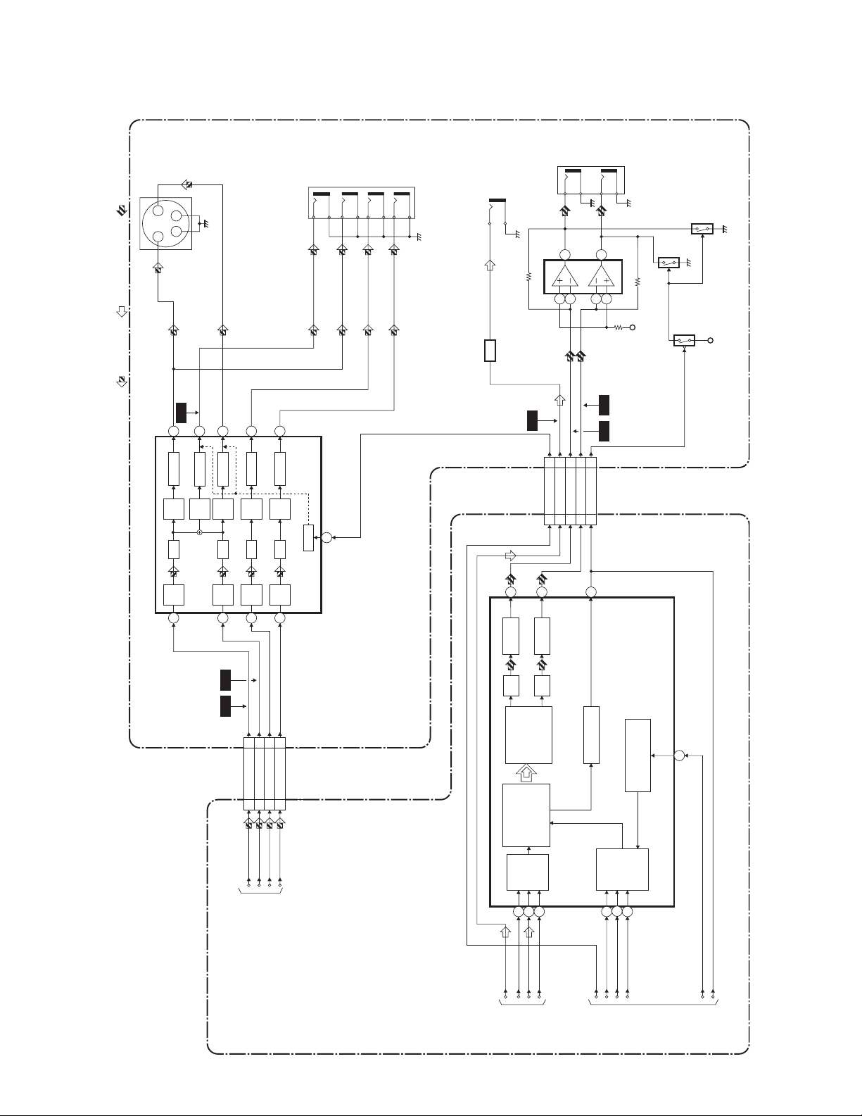
Video / Audio Block Diagram
JK1401
S-VIDEO OUT
AUDIO SIGNALDATA(AUDIO) SIGNAL
2
1
3 4
YC
VIDEO SIGNAL
VIDEO OUT
JK1404
(COMPOSITE)
VIDEO-Y
OUT
VIDEO-Cb/Pb
OUT
VIDEO-Cr/Pr
OUT
DIGITAL
JK1202
AMP
Q1351
AUDIO OUT
(COAXIAL)
(AMP)
IC1201
JK1404
1
3
AUDIO(L)-
OUT
2
AUDIO(R)-
7
5
6
OUT
+5V
Q1202
Q1204
Q1201
+3.3V
WF3
18
2dB
AMP
2dB
LPF DRIVER
4dB
AMP
IC1402 (VIDEO DRIVER)
6
21
DRIVER
AMP
23
2dB
AMP
LPF DRIVER
4dB
AMP
2
WF1 WF2
15
2dB
AMP
LPF DRIVER
4dB
AMP
9
88VIDEO-Y(I/P)
10 10VIDEO-C
CN601 CN1601
13
2dB
AMP
LPF DRIVER
4dB
AMP
11
66VIDEO-Cb/Pb
44VIDEO-Cr/Pr
MUTE
WF6
2
18
SPDIF
I/P-SW
2
18
15
L-CH
LPF+AMP
DAC
ENHANCED
MULTI-LEVEL
CN601 CN1601
14
R-CH
LPF+AMP
DAC
MODULATOR
DELTA-SIGMA
3
15
AUDIO(R)
13 13AUDIO(L)
15
WF4 WF5
AUDIO(R)-MUTE
14 14
16
ZERO DETECT
5
MANAGER
SYSTEM CLOCK
DVD MAIN CBA UNIT AV CBA
4X/8X
/FUNCTION
CONTROLLER
DIGITAL FILTER
OVERSAMPLING
VIDEO-Y(I/P)
VIDEO-C
VIDEO-Cb/Pb
VIDEO-Cr/Pr
TO DIGITAL
SIGNAL PROCESS
BLOCK DIAGRAM
1-8-3
ADAC-MD
I/P-SW
SERIAL
CONTROL
432
ADAC-MC
ADAC-ML
PORT
TO
SYSTEM
CONTROL
/SERVO
BLOCK
DIAGRAM
PCM-SCLK
AUDIO-MUTE
PORT
AUDIO
SERIAL
IC601 (AUDIO DAC)
768
PCM-BCK
SPDIF
PCM-DATA
PCM-LRCLK
TO
DIGITAL
SIGNAL
PROCESS
BLOCK
DIAGRAM
E6121BLV
Page 20
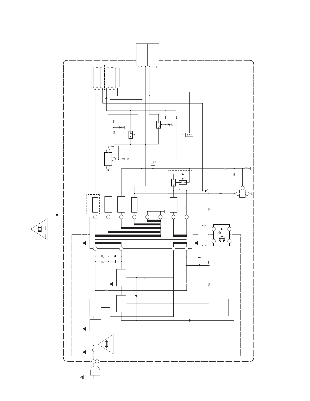
Power Supply Block Diagram
NOTE:
The voltage for parts in hot circuit is measured using
hot GND as a common terminal.
EV+1.2V
TO CN401
4,5
CN1001
EV+3.3V
6,7,8
EV+10V10P-ON+5V9P-ON+3.3V20PWRCON
11,12
-FL
DVL700F
"Ce symbole reprèsente un fusible à fusion rapide."
"This symbol means fast operating fuse."
CAUTION !
For continued protection against fire hazard,
replace only with the same type fuse.
ATTENTION : Pour une protection continue les risqes
d'Incele n'utiliser que des fusible de même type.
Risk of fire-replace fuse as marked.
D1003
RECTIFIER
DVL70 0FDVL70 0F
DVL70 0F
11
F
A V
T1001
2
F1
P-ON+9V
F2
2
+1.2V
IC1002
3
3
SCHOTTKY
D1006
12
EV+5V
EV+3.3V
1
REG.
BARRIER
D1008
P-ON+5V
SCHOTTKY
BARRIER
13
4
Q1002
D1030
RECTIFIER
14
15
Q1011
Q1004
Q1016
Q1015
Q1005
DVL700F
312
REG
2
3
IC1006
(SHUNT REGULATOR)
D1016
RECTIFIER
16
17
18
1
4
IC1001
ERROR
7
6
VOLTAGE DET
HOT CIRCUIT. BE CAREFUL.
CAUTION !
Fixed voltage (or Auto voltage selectable) power supply circuit is used in this unit.
If Main Fuse (F1001) is blown , check to see that all components in the power supply
circuit are not defective before you connect the AC plug to the AC power supply.
Otherwise it may cause some components in the power supply circuit to fail.
BRIDGE
RECTIFIER
D1001, D1002
D1004, D1005
LINE
FILTER
L1001
1A 250V
F1001
AC1001
AC CORD
F
SWITCHING
Q1031
SWITCHING
Q1003
A V
CONTROL
1-8-4
AV CBA
HOT
E6121BLP
Page 21

SCHEMATIC DIAGRAMS / CBA’S AND TEST POINTS
Standard Notes
WARNING
Many electrical and mechanical parts in this chassis
have special characteristics. These characteristics
often pass unnoticed and the protection afforded by
them cannot necessarily be obtained by using
replacement components rated for higher voltage,
wattage, etc. Replacement parts that have these
special safety characteristics are identified in this
manual and its supplements; electrical components
having such features are identified by the mark “#” in
the schematic diagram and the parts list. Before
replacing any of these components, read the parts list
in this manual carefully. The use of substitute
replacement parts that do not have the same safety
characteristics as specified in the parts list may create
shock, fire, or other hazards.
Notes:
1. Do not use the part number shown on these
drawings for ordering. The correct part number is
shown in the parts list, and may be slightly
different or amended since these drawings were
prepared.
2. All resistance values are indicated in ohms
(K = 10
3. Resistor wattages are 1/4W or 1/6W unless
otherwise specified.
4. All capacitance values are indicated in µF
(P = 10
5. All voltages are DC voltages unless otherwise
specified.
3
, M = 106).
-6
µF).
1-9-1 E6N_SC
Page 22
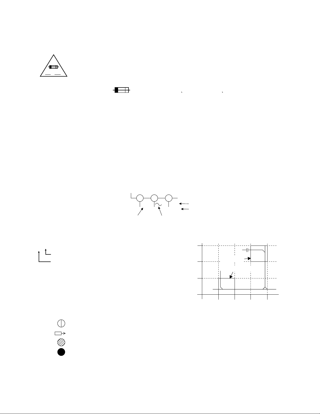
LIST OF CAUTION, NOTES, AND SYMBOLS USED IN THE SCHEMATIC DIAGRAMS ON
THE FOLLOWING PAGES:
1. CAUTION:
FOR CONTINUED PROTECTION AGAINST FIRE HAZARD, REPLACE ONLY WITH THE
F
A V
SAME TYPE FUSE.
ATTENTION: POUR UNE PROTECTION CONTINUE LES RISQES D'INCELE N'UTILISER
QUE DES FUSIBLE DE MÊME TYPE.
RISK OF FIRE-REPLACE FUSE AS MARKED.
This symbol means fast operating fuse.
Ce symbole represente un fusible a fusion rapide.
2. CAUTION:
Fixed Voltage (or Auto voltage selectable) power supply circuit is used in this unit.
If Main Fuse (F1001) is blown, first check to see that all components in the power supply circuit are not
defective before you connect the AC plug to the AC power supply. Otherwise it may cause some components
in the power supply circuit to fail.
3. Note:
1. Do not use the part number shown on the drawings for ordering. The correct part number is shown in the
parts list, and may be slightly different or amended since the drawings were prepared.
2. To maintain original function and reliability of repaired units, use only original replacement parts which are
listed with their part numbers in the parts list section of the service manual.
4. Voltage indications for PLAY and STOP mode on the schematics are as shown below:
2
1
(Unit: Volt)
The same voltage for
both PLAY & STOP modes
5.0
3
5.0
(2.5)
Indicates that the voltage
is not consistent here.
PLAY mode
STOP mode
5. How to read converged lines
1-D3
Distinction Area
Line Number
(1 to 3 digits)
Examples:
1. "1-D3" means that line number "1" goes to the line number
"1" of the area "D3".
2. "1-B1" means that line number "1" goes to the line number
"1" of the area "B1".
3
AREA D3
2
1
ABCD
AREA B1
1-D3
1-B1
6. Test Point Information
: Indicates a test point with a jumper wire across a hole in the PCB.
: Used to indicate a test point with a component lead on foil side.
: Used to indicate a test point with no test pin.
: Used to indicate a test point with a test pin.
1-9-2 E6N_SC
Page 23
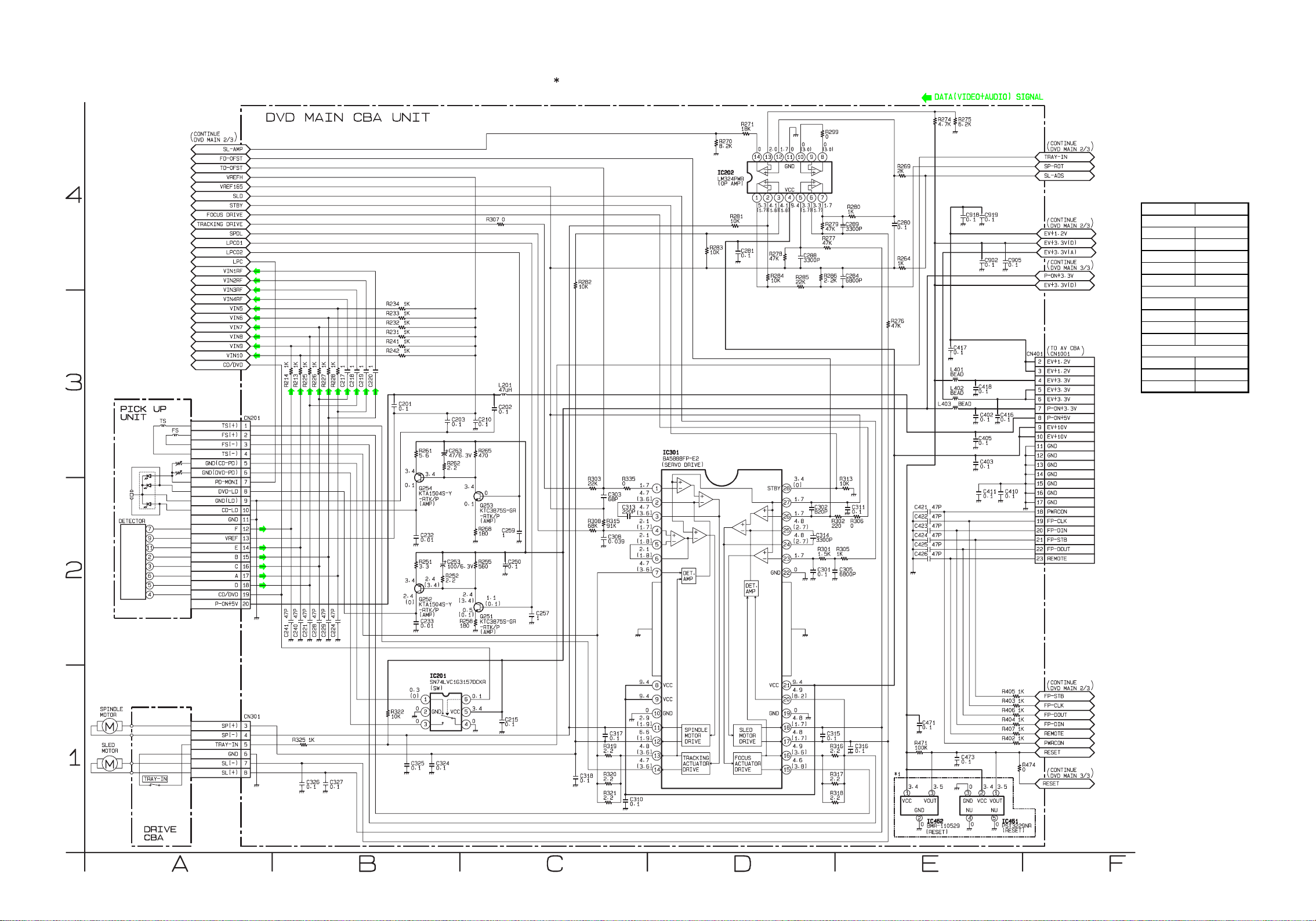
DVD Main 1/3 Schematic Diagram
DVD MAI N 1/3
Ref No. Pos it ion
IC201 C-1
IC202 D-4
IC301 D-3
IC461 F-1
IC462 E-1
Q251 C-2
Q252 B-2
Q253 C-2
Q254 B-2
CN201 A-3
CN301 A-1
CN401 F-3
CONNECTORS
ICS
TRANSISTORS
1 NOTE:
Either IC461 or IC462 is used for DVD MAIN CBA UNIT.
1-9-3
E6121SCD1
Page 24
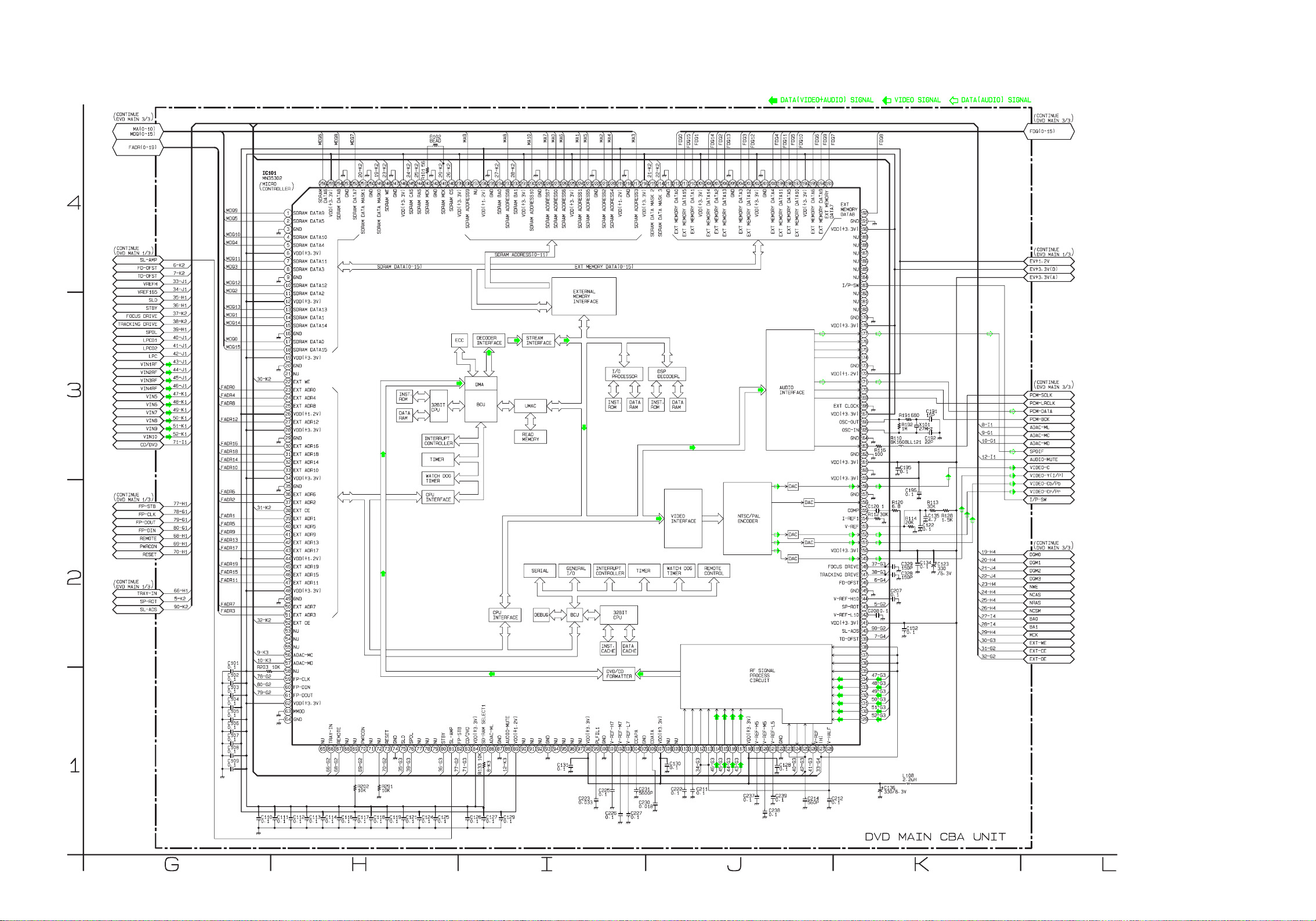
DVD Main 2/3 Schematic Diagram
1-9-4
E6121SCD2
Page 25
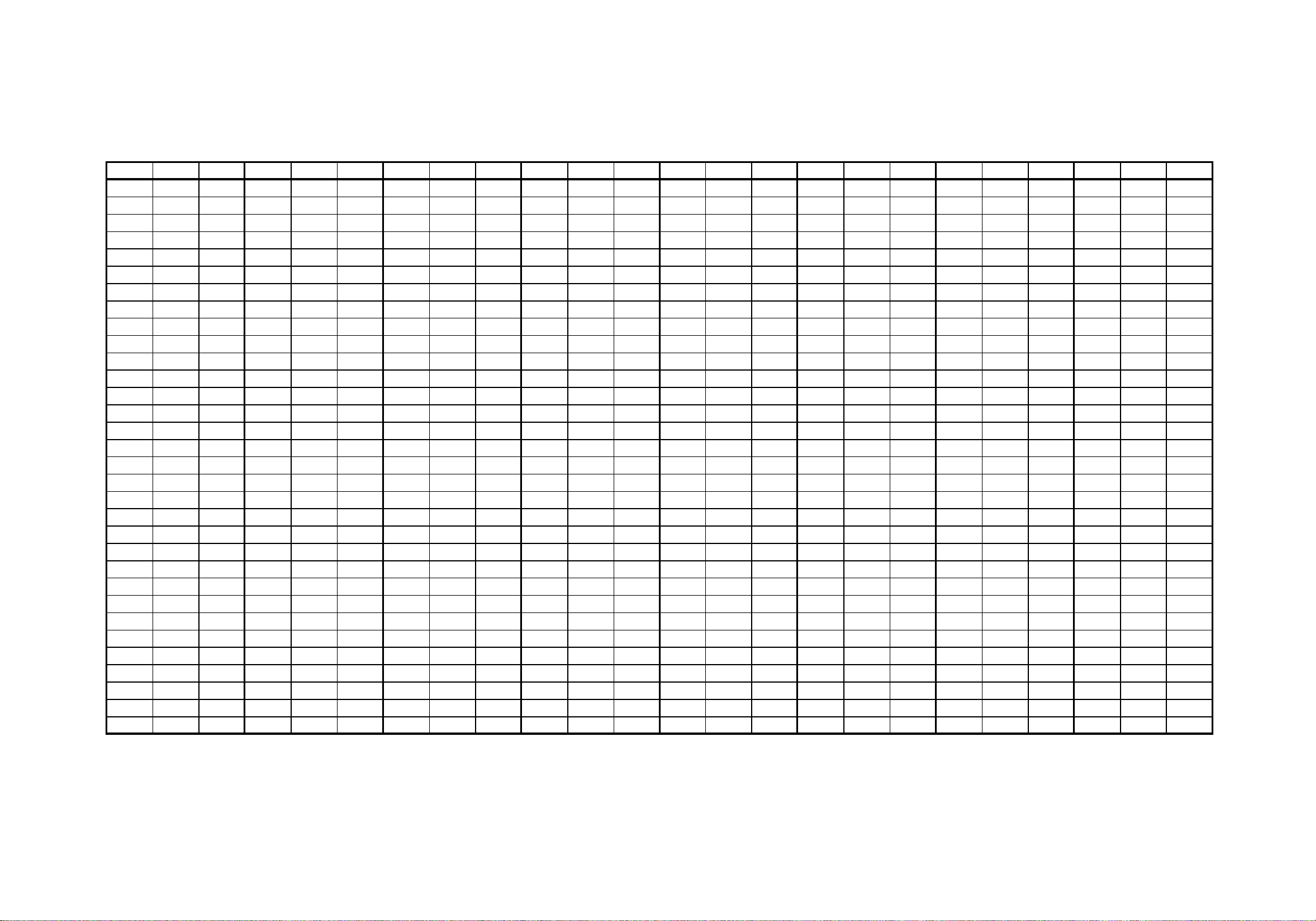
IC101 Voltage Chart
PIN.NO PLAY STOP PIN.NO PLAY STOP PIN.NO PLAY STOP PIN.NO PLAY STOP
129 2.3 2.3 161 3.4 3.4 193 ~ ~ 225 3.4 3.4
130 2.3 2.3 162 0 0 194 ~ ~ 226 ~ ~
131 2.3 2.3 163 1.8 1.8 195 ~ ~ 227 ~ ~
132 2.4 2.3 164 0 0 196 3.4 3.4 228 ~ ~
133 2.4 2.4 165 1.7 1.8 197 ~ ~ 229 0 0
134 2.4 2.4 166 1.7 1.7 198 ~ ~ 230 ~ ~
135 2.3 2.3 167 3.4 3.4 199 ~ ~ 231 3.4 3.4
136 2.3 2.3 168 0 0 200 ~ ~ 232 1.3 1.6
137 2.3 2.3 169 1.8 1.8 201 0 0 233 ~ ~
138 2.3 2.3 170 1.7 1.7 202 3.4 3.4 234 1.9 2.3
139 1.7 1.7 171 1.3 0.1 203 ~ ~ 235 0 0
140 1.7 1.7 172 1.3 1.3 204 ~ ~ 236 1.3 1.3
141 3.4 3.4 173 0 0 205 0 0 237 ----- -----
142 1.3 1.3 174 ----- ----- 206 ~ ~ 238 ~ ~
143 2.1 1.7 175 ----- ----- 207 ~ ~ 239 3.4 3.4
144 2.2 2.2 176 ----- ----- 208 ~ ~ 240 3.4 3.3
145 0 0 177 1.8 1.7 209 3.4 3.4 241 1.9 1.9
146 1.7 1.7 178 3.4 3.5 210 ~ ~ 242 0 0
147 1.8 1.7 179 0 0 211 ~ ~ 243 1.9 1.9
148 1.7 1.7 180 ----- ----- 212 ~ ~ 244 3.4 3.3
149 0.6 0.5 181 ----- ----- 213 0 0 245 3.4 3.4
150 3.4 3.4 182 ----- ----- 214 ~ ~ 246 3.4 3.4
151 0.5 0.5 183 3.4 3.4 215 ~ ~ 247 0 0
152 0.5 0.5 184 ----- ----- 216 3.4 3.4 248 3.3 3.4
153 1.4 1.3 185 ----- ----- 217 ~ ~ 249 3.2 3
154 1.4 1.3 186 ----- ----- 218 0 0 250 0 0
155 2.4 2.4 187 ----- ----- 219 1.3 1.3 251 3.2 3.0
156 ----- ----- 188 ----- ----- 220 ~ ~ 252 ~ ~
157 0 0 189 ----- ----- 221 ~ ~ 253 0 0
158 0.9 0.9 190 3.4 3.5 222 0 0 254 ~ ~
159 3.4 3.4 191 0 0 223 ~ ~ 255 3.4 3.4
160 0 0 192 ~ ~ 224 ~ ~ 256 ~ ~
~ : Volt age is not consis tent ----- : Not used Unit : Volts
PIN.NO PLAY STOP PIN.NO PLAY STOP PIN.NO PLAY STOP PIN.NO PLAY STOP
1 ~ ~ 33 ~ ~ 65 ----- ----- 97 ----- -----
2 ~ ~ 343.43.4663.43.5983.43.4
3 0 0 35 0 0 673.23.2990.90.8
4 ~ ~ 36 ~ ~ 68 ----- ----- 100 0 0
5 ~ ~ 37 ~ ~ 69 3.4 3.4 101 2.4 2.4
6 3.4 3.4 38 0.4 0.3 70 3.4 3.4 102 2.2 2.2
7 ~ ~ 39 ~ ~ 71 ----- ----- 103 1.9 1.9
8 ~ ~ 40 ~ ~ 72 1.4 2.7 104 0.4 0.3
9 0 0 41 ~ ~ 73 3.5 3.5 105 0 0
10 ~ ~ 42 ~ ~ 74 0 0 106 1.7 1.7
11 ~ ~ 43 ~ ~ 75 1.7 1.8 107 3.4 3.4
12 3.4 3.4 44 1.3 1.3 76 2.3 1.8 108 ----- -----
13 ~ ~ 45 ~ ~ 77 ----- ----- 109 ----- -----
14 ~ ~ 46 ~ ~ 78 ----- ----- 110 1.9 1.9
15 ~ ~ 47 ~ ~ 79 ----- ----- 111 1.9 1.9
16 0 0 48 3.4 3.4 80 3.4 0 112 1.7 1.7
17 ~ ~ 49 0 0 81 0.1 0.1 113 1.7 1.7
18 ~ ~ 50 ~ ~ 82 2.8 2.8 114 1.7 1.7
19 3.4 3.4 51 ~ ~ 83 0.1 0.1 115 1.7 1.7
20 0 0 52 0.8 0.8 84 3.4 3.4 116 1.7 1.7
21 ----- ----- 53 ----- ----- 85 0.1 0.1 117 1.7 1.7
22 3.4 3.4 54 ----- ----- 86 3.6 3.4 118 3.4 3.4
23 ~ ~ 55 ----- ----- 87 0 0 119 2.0 2.0
24 ~ ~ 56 3.4 3.4 88 3.5 0.1 120 1.7 1.7
25 ~ ~ 57 3.5 3.5 89 1.3 1.3 121 1.5 1.5
26 1.3 1.3 58 3.4 3.4 90 ----- ----- 122 0 0
27 ~ ~ 59 3.4 3.4 91 ----- ----- 123 0.3 0.1
28 3.4 3.4 60 3.4 3.4 92 ----- ----- 124 1.1 0.1
29 0 0 61 3.5 3.5 93 0 0 125 0.3 0.1
30 ~ ~
31 ~ ~
32 ~ ~
62 3.4 3.4
63 0 0
64 0 0
94 ----- ----- 126 0.1 0.1
95 ----- ----- 127 2.3 2.3
96 ----- ----- 128 1.7 1.7
1-9-5
Page 26
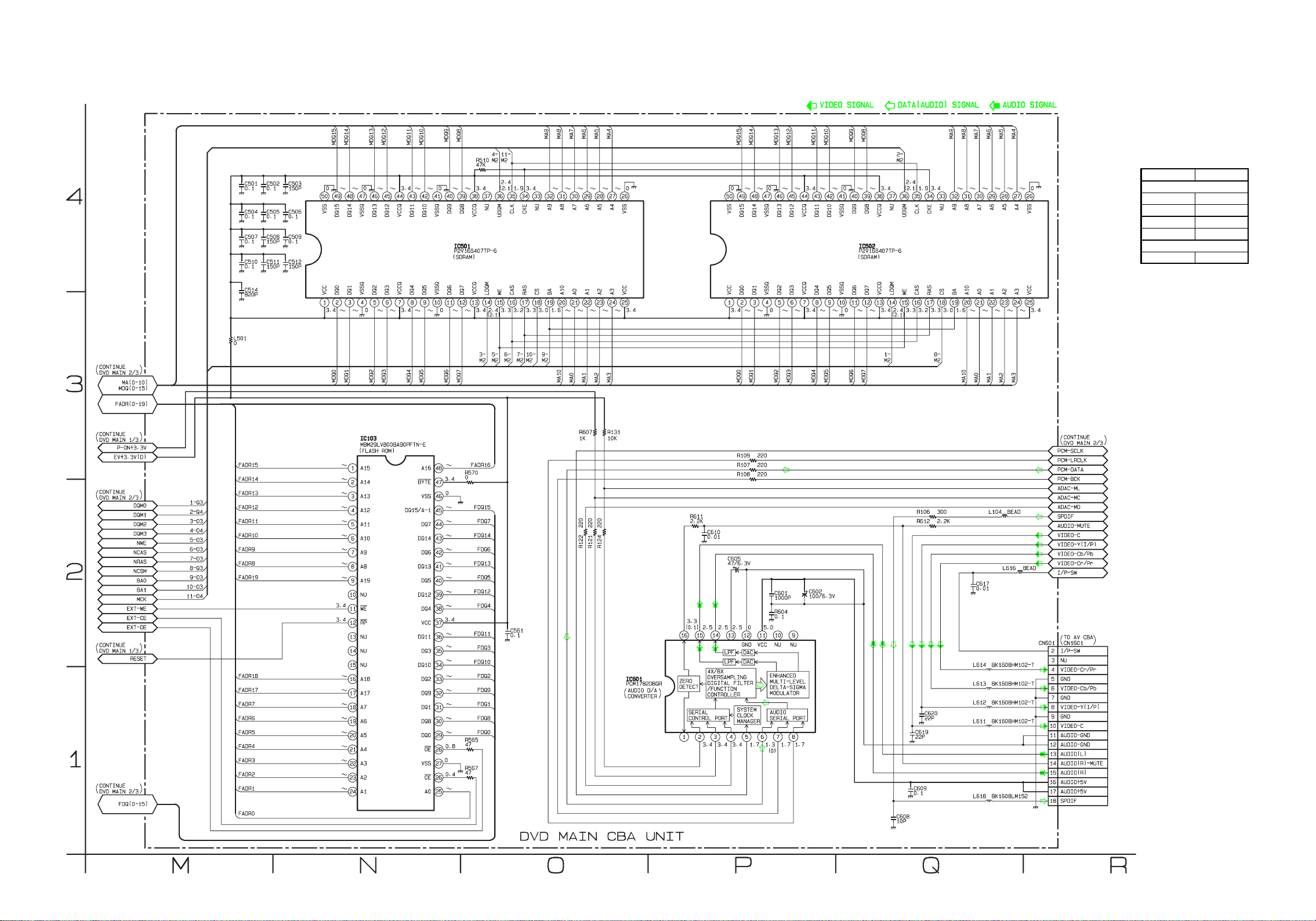
DVD Main 3/3 Schematic Diagram
DVD MAI N 3/3
Ref No. Pos it ion
IC103 N-3
IC501 O-4
IC502 Q-4
IC601 O-1
CN601 R-2
ICS
CONNECTOR
1-9-6
E6121SCD3
Page 27
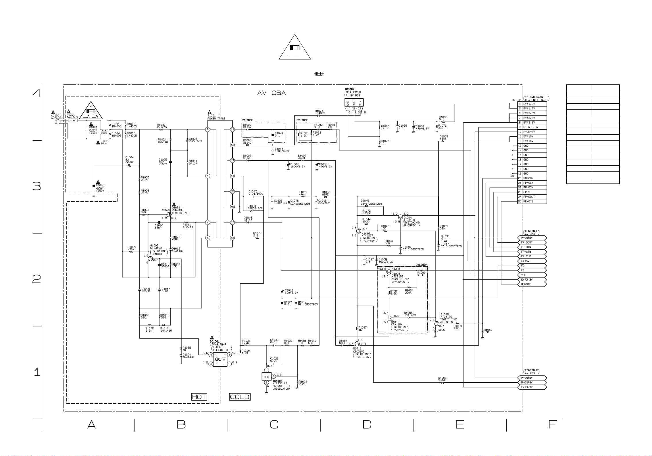
AV 1/3 Schematic Diagram
"Ce symbole reprèsente un fusible à fusion rapide."
CAUTION !
For continued protection against fire hazard,
replace only with the same type fuse.
ATTENTION : Pour une protection continue les risqes
d'Incele n'utiliser que des fusible de même type.
Risk of fire-replace fuse as marked.
"This symbol means fast operating fuse."
A V
F
AV 1/3
Ref No. Position
IC1001 B-1
IC1002 D-4
IC1006 C-1
Q1002 D-3
Q1003 B-2
Q1004 D-3
Q1005 D-2
Q1011 D-1
Q1015 D-2
Q1016 E-2
Q1031 B-3
CN1001 F-4
ICS
TRANSISTORS
CONNECTOR
CAUTION !
Fixed voltage (or Auto voltage selectable) power supply circuit is used in this unit.
If Main Fuse (F1001) is blown , check to see that all components in the power supply
circuit are not defective before you connect the AC plug to the AC power supply.
Otherwise it may cause some components in the power supply circuit to fail.
NOTE:
The voltage for parts in hot circuit is measured using
hot GND as a common terminal.
1-9-7
E6121SCAV1
Page 28
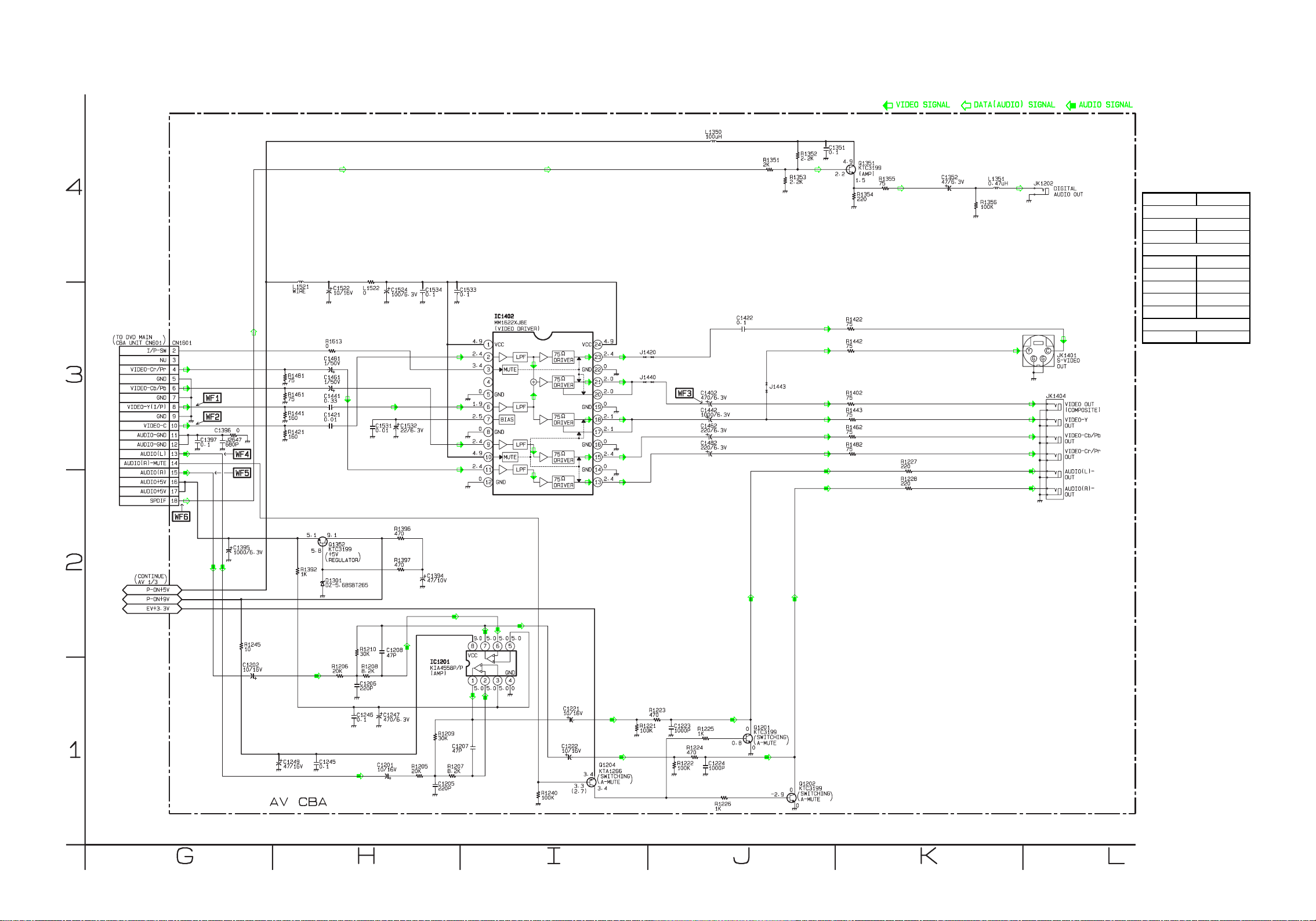
AV 2/3 Schematic Diagram
AV 2/3
Ref No. Position
IC1201 H-1
IC1402 I-3
Q1201 J-1
Q1202 J-1
Q1204 I -1
Q1351 K-4
Q1352 H-2
CN1601 G-3
ICS
TRANSISTORS
CONNECTOR
1-9-8
E6121SCAV2
Page 29
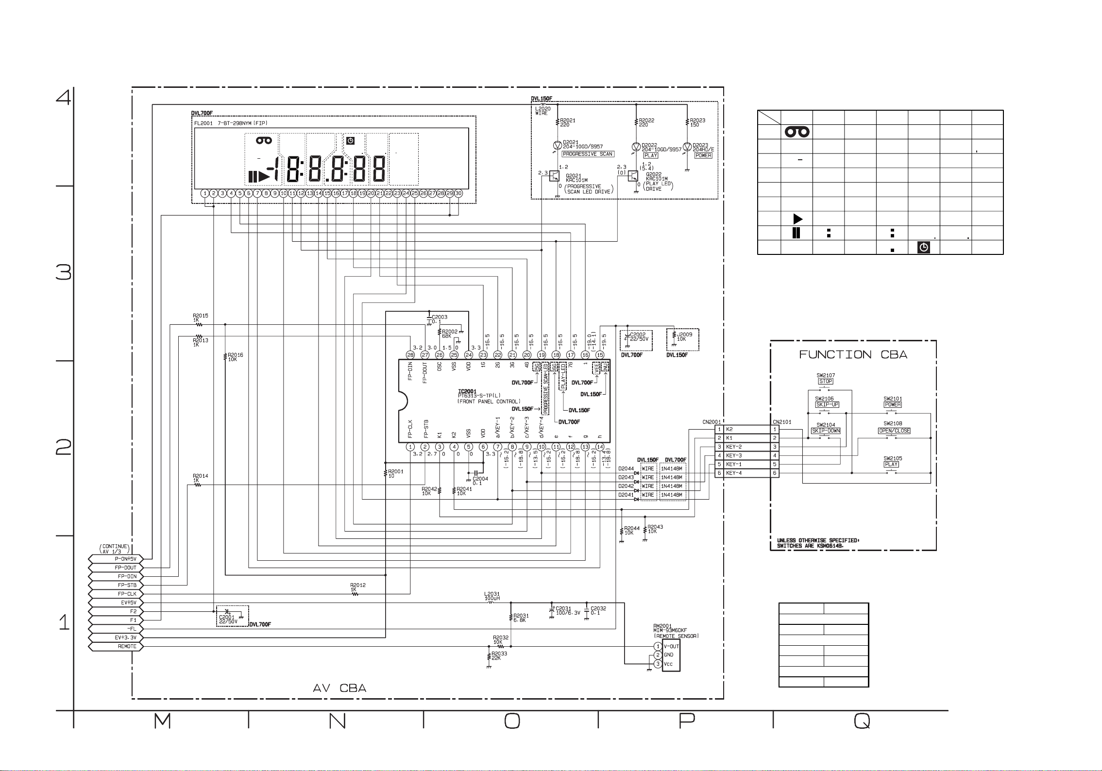
AV 3/3 & Function Schematic Diagram
7G 6G 5G 4G 3G 2G 1G
a
b
c
d
e
f
g
c
d
e
ff
g
c
d
e
f
g
c
d
e
f
g
c
d
e
f
g
c
d
e
f
g
h
ii
a
b
a
b
a
b
a
b
a
b
FL2001 MATRIX CHART
REPEAT
TITLE
GROUP
VCR
CHP
REC
SACD
TRK
ALL
B
PSCAN
DVD
P
M
HD
V
CD
A
A
AV 3/3
Ref No. Position
IC2001 O-2
Q2021 O-4
Q2022 P-4
CN2001 P-2
IC
TRANSISTORS
CONNECTOR
7G
REPEAT
B
A
ALL
f
6G
TITLE
i
i
5G 4G 3G 2G 1G
CHP
REC
TRK
a
c
d
g
VCR
GROUP
SACD
PSCAN
DVD
b
PM
ef
HDVCD
A
1-9-9
E6121SCAV3
Page 30
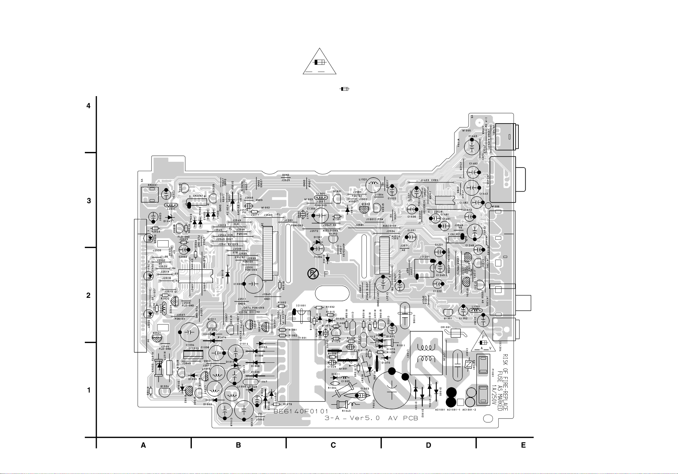
AV CBA Top View
"Ce symbole reprèsente un fusible à fusion rapide."
CAUTION !
For continued protection against fire hazard,
replace only with the same type fuse.
ATTENTION : Pour une protection continue les risqes
d'Incele n'utiliser que des fusible de même type.
Risk of fire-replace fuse as marked.
"This symbol means fast operating fuse."
A V
F
CAUTION !
Fixed voltage (or Auto voltage selectable) power supply circuit is used in this unit.
If Main Fuse (F1001) is blown , check to see that all components in the power supply
circuit are not defective before you connect the AC plug to the AC power supply.
Otherwise it may cause some components in the power supply circuit to fail.
NOTE:
The voltage for parts in hot circuit is measured using
hot GND as a common terminal.
1-9-10
BE6140F01013-A
Page 31
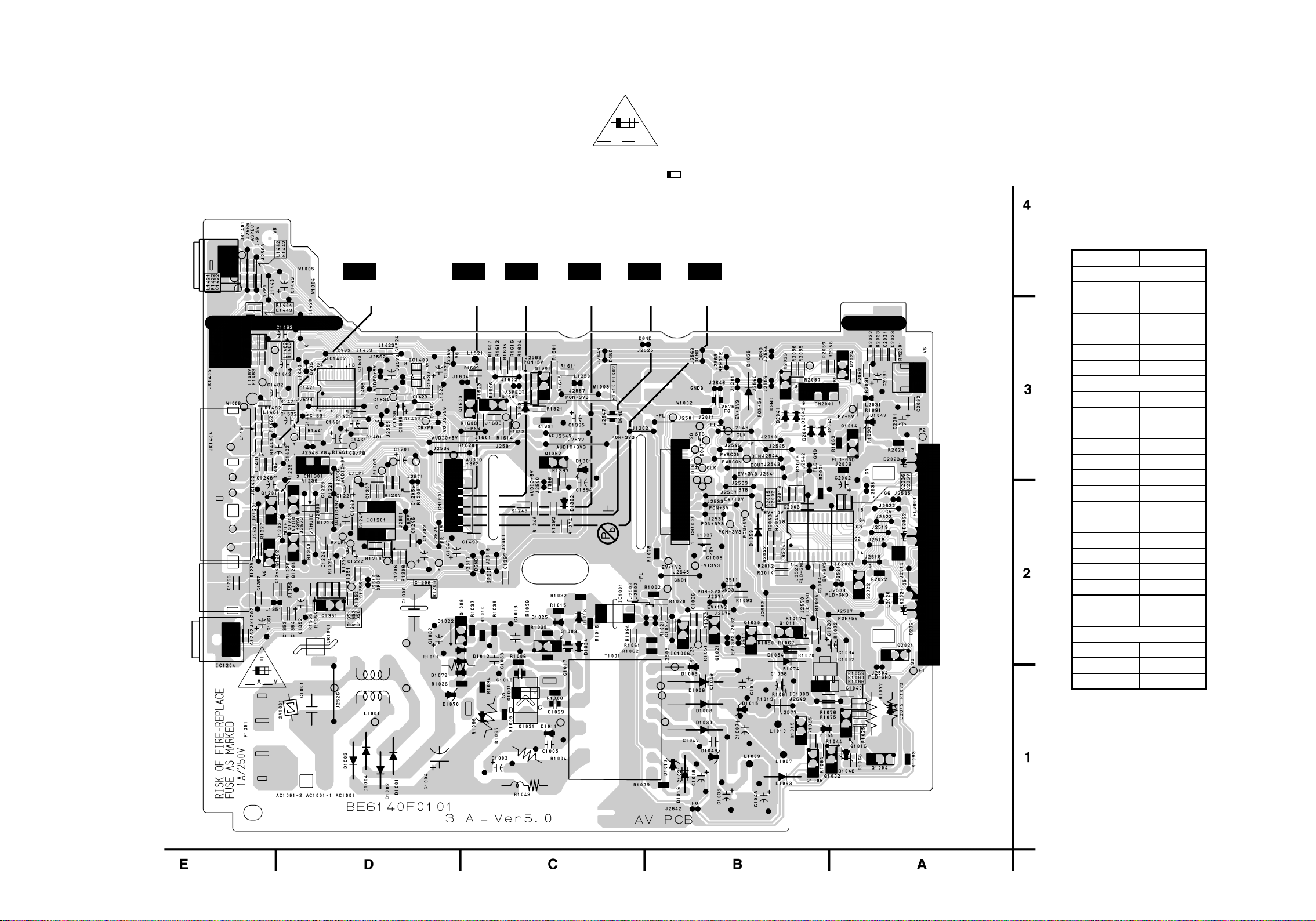
AV CBA Bottom View
"Ce symbole reprèsente un fusible à fusion rapide."
CAUTION !
For continued protection against fire hazard,
replace only with the same type fuse.
ATTENTION : Pour une protection continue les risqes
d'Incele n'utiliser que des fusible de même type.
Risk of fire-replace fuse as marked.
"This symbol means fast operating fuse."
A V
F
AV CBA
Ref No. Position
IC1001 C-2
IC1002 A-2
IC1006 B-2
IC1201 D-2
IC1403 D-3
IC2001 A-2
Q1002 A-1
Q1003 C-2
Q1004 A-1
Q1005 B-1
Q1011 B-2
Q1015 B-1
Q1016 A-1
Q1031 C-1
Q1201 E-2
Q1202 D-2
Q1204 D-2
Q1351 D-2
Q1352 C-3
Q2021 A-2
Q2022 A-2
CN1001 B-2
CN1601 D-2
CN2001 B-3
ICS
TRANSISTORS
CONNECTORS
CAUTION !
Fixed voltage (or Auto voltage selectable) power supply circuit is used in this unit.
If Main Fuse (F1001) is blown , check to see that all components in the power supply
circuit are not defective before you connect the AC plug to the AC power supply.
Otherwise it may cause some components in the power supply circuit to fail.
WF3
C1402
PLUS LEAD
WF1
PIN 8 OF
CN1601
WF2
PIN 10 OF
CN1601
WF4
PIN 13 OF
CN1601
WF5
PIN 15 OF
CN1601
NOTE:
The voltage for parts in hot circuit is measured using
hot GND as a common terminal.
WF6
PIN 18 OF
CN1601
1-9-11
BE6140F01013-A
Page 32
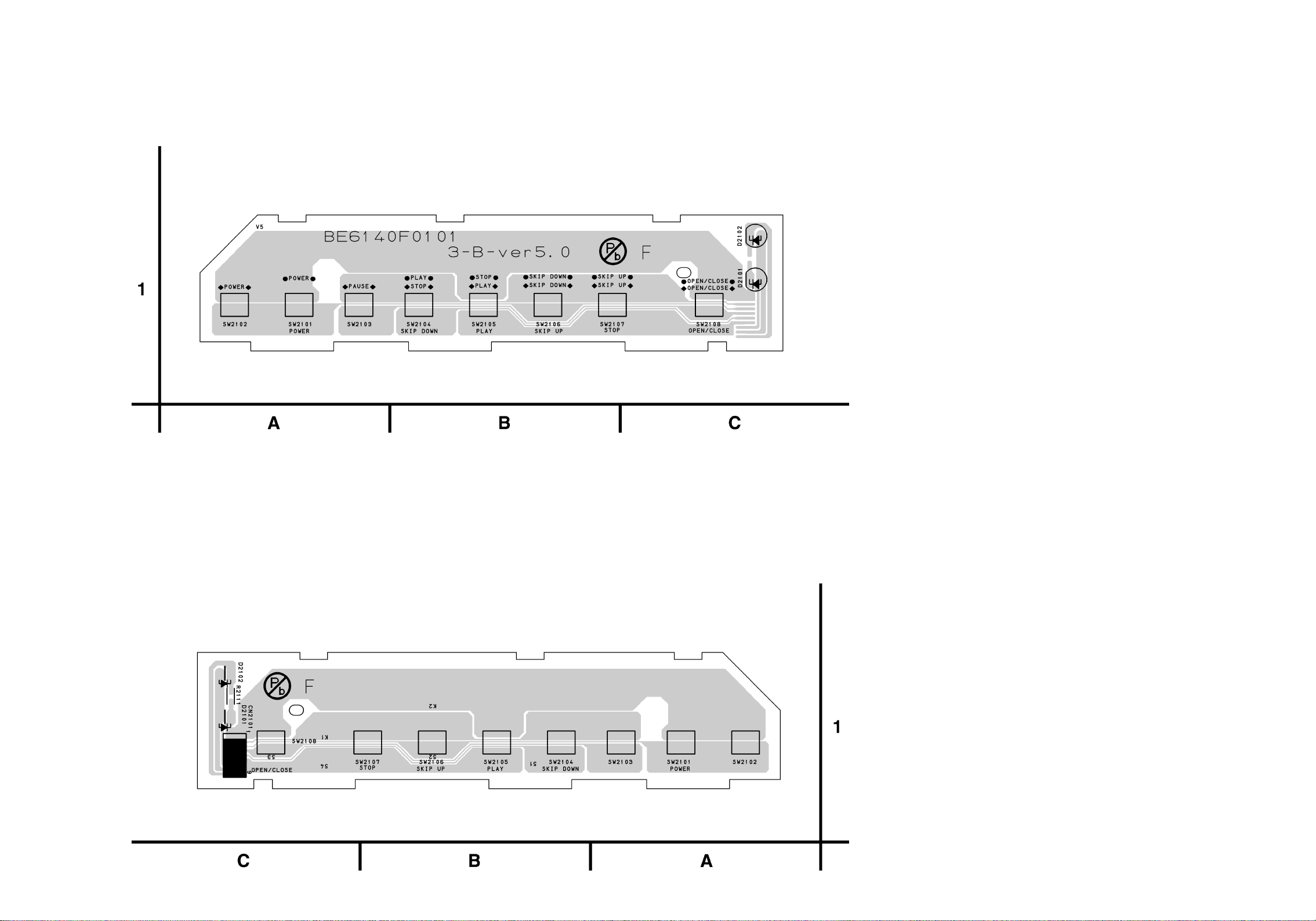
FUNCTION CBA Top View
FUNCTION CBA Bottom View
1-9-12
BE6140F01013-B
Page 33
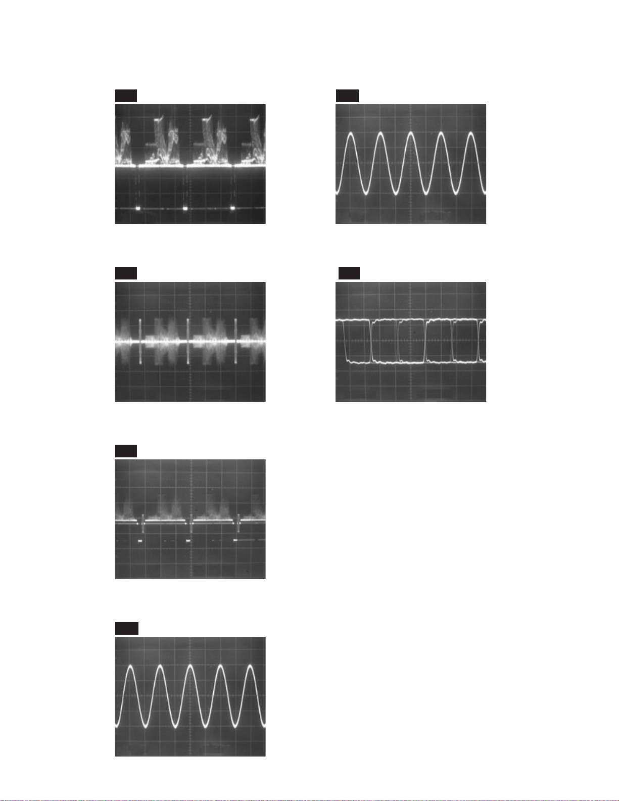
WAVEFORMS
0.1V
VIDEO-Y
VIDEO-C
0.1V
VIDEO-CVBS
0.5V
AUDIO(L)
1V
0.5ms
AUDIO(R)
1V
0.5ms
SPDIF
1V
0.1
WF1
Pin 8 of CN1601
VIDEO-Y
WF2
Pin 10 of CN1601
2020µ
s0.1V
WF5
Pin 15 of CN1601
AUDIO(R)
WF6
Pin 18 of CN1601
1V
0.5ms
VIDEO-C
WF3
C1402 PLUS LEAD
VIDEO-CVBS
WF4
Pin 13 of CN1601
0.1V
0.5V
2020µ
2020µ
s
s
SPDIF
1V
0.1
µ
s
NOTE:
Input
CD: 1kHz PLAY
(WF4~WF6)
DVD: POWER ON (STOP) MODE
(WF1~WF3)
AUDIO(L)
1V
0.5ms
1-10-1
E6121WF
Page 34
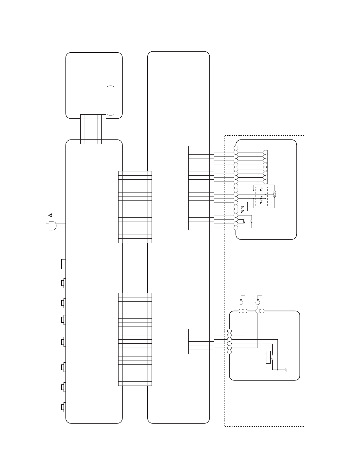
FUNCTION CBA
CN2101 is soldered
WIRING DIAGRAM
directly to the PCB.
AC CORD
S-VIDEO
OUT
DIGITAL
AUDIO OUT
(COAXIAL)
AUDIO(R)-
OUT
AUDIO(L)-
OUT
VIDEO OUT
(COMPOSITE)
VIDEO-Cr/Pr
OUT
VIDEO-Cb/Pb
OUT
K2 11K1 22KEY-2 33KEY-3 44KEY-1 55KEY-4 6
CN2001 CN2101
AV CBA
6
I/P-SW 22
NU 33
VIDEO-Cr/Pr 44
GND 55
VIDEO-Cb/Pb 66
GND 77
VIDEO-Y(I/P) 88
GND 99
VIDEO-C 1010
AUDIO-GND 1111
CN1601
AUDIO-GND 1212
AUDIO(L) 1313
AUDIO(R)-MUTE
AUDIO(R) 1515
AUDIO+5V 1616
(CN1601 is soldered directly to the PCB.)
AUDIO+5V 1717
SPDIF 1818
EV+1.2V 24
EV+1.2V 35
EV+3.3V 46
EV+3.3V 57
EV+3.3V 68
P-ON+3.3V 79
P-ON+5V 810
EV+10V 911
EV+10V 1012
GND 1113
GND 1214
GND 1315
CN1001
GND 1416
GND 1517
GND 1618
GND 1719
PWRCON 1820
(CN1001 is soldered directly to the PCB.)
FP-CLK 1921
FP-DIN 2022
FP-STB 2123
FP-DOUT 2224
REMOTE
P-ON+5V
20
CD/DVD
19
D
18
A
17
C
16
B
15
E
14
VREF
13
F
12
GND
11
CD-LD
GND(LD)
DVD-LD
PD-MONI
TS(-)
FS(-)
FS(+)
TS(+)
10
9
8
7
6
5
4
3
2
1
FS
CN201CN301
CN601
1414
GND(DVD-PD)
GND(CD-PD)
DVD MAIN CBA UNIT
M
SLED
MOTORMSPINDLE
SL(+)
8
SL(-)
7
GND
CN401
2325
TRAY-IN
SP(-)
SP(+)
6
5
4
3
4
DETECTOR
7 9 11 2 3 6 5
PICK UP UNIT
TS
DVD MECHANISM
MOTOR
DRIVE CBA
TRAY-IN
VIDEO-Y
OUT
1-11-1
E6121WI
Page 35
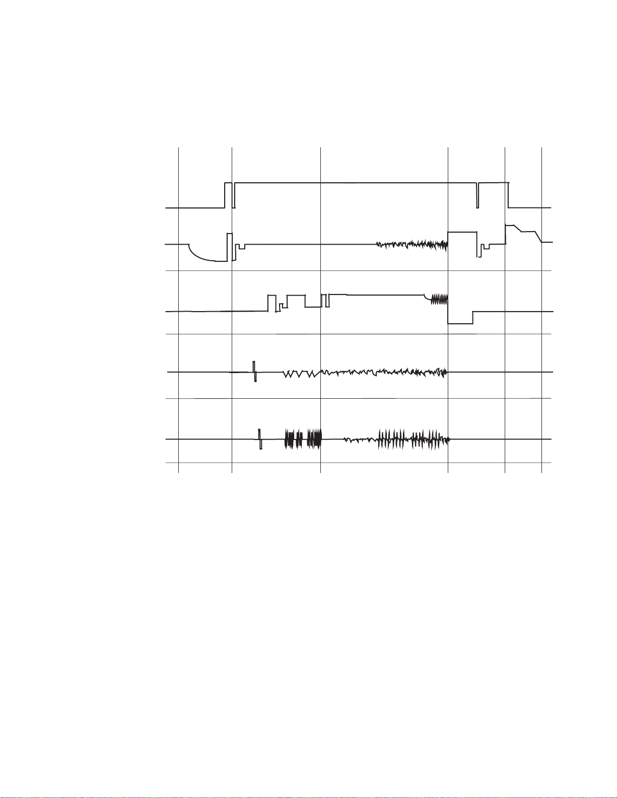
SYSTEM CONTROL TIMING CHARTS
Tray Close ~ Play / Play ~ Tray Open
Tray IN
(TL221)
Sled Drive
(TP303)
Disc Drive
(TP301)
Focus Drive
(TP304)
Tracking Drive
(TP302)
3.3V
0V
1.65V
0V
1.65V
0V
1.65V
0V
1.65V
0V
Tr ay
Close
Disc
Rotation
Play
Disc
Stop
Tr ay
Open
1-12-1 E6NTI
Page 36
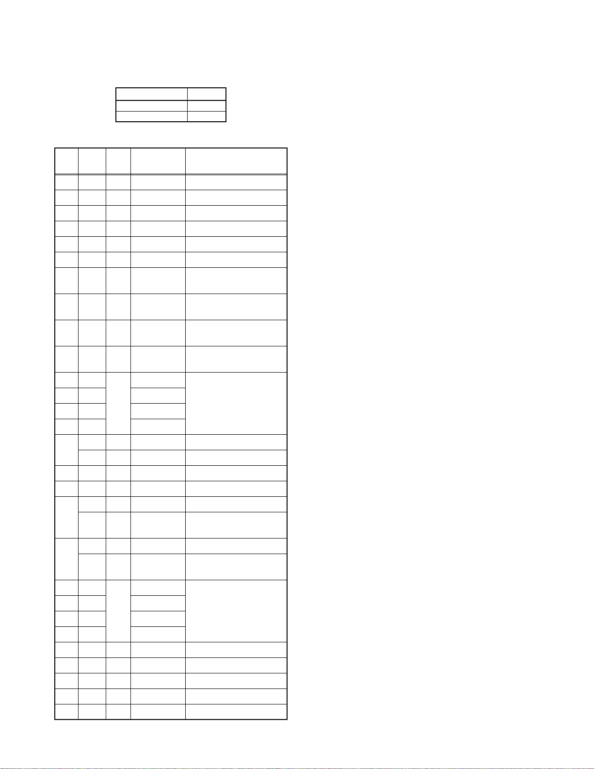
IC PIN FUNCTION DESCRIPTIONS
Comparison Chart of Models and Marks
Model Mark
DVL700F A
DVL150F B
IC2001 (FRONT PANEL CONTROL)
Pin
Mark
No.
1 IN FP-CLK Clock Input
2 IN FP-STB Serial Interface Strobe
3 IN K1 Key Data 1 Input
4 IN K2 Key Data 2 Input
5- VSSGND
6 - VDD Power Supply
7OUTa / KEY-1
8OUTb / KEY-2
9OUTc / KEY-3
10 OUT d / KEY-4
11
12 f
13 g
14 h
15
16 OUT i Segment Output
17 OUT 7G Grid Output
18
19
20
21 3G
22 2G
23 1G
24 - VDD Power Supply
25 - VSS GND
26 IN OSC Oscillator Input
27 OUT FP-DOUT Serial Data Output
28 IN FP-DIN Serial Data Input
IN/
OUT
OUT
A - VEE Pull Down Level
B - NU Not Used
A OUT 6G Grid Output
B OUT PLAY-LED
A OUT 5G Grid Output
BOUT
OUT
Signal
Name
e
DISC-INLED
4G
Function
Segment Output / Key
Source-1
Segment Output / Key
Source-2
Segment Output / Key
Source-3
Segment Output / Key
Source-4
Segment Output
“PLAY” LED Signal
Output
“DISC-IN” LED Signal
Output
Grid Output
1-13-1 E6121PIN
Page 37
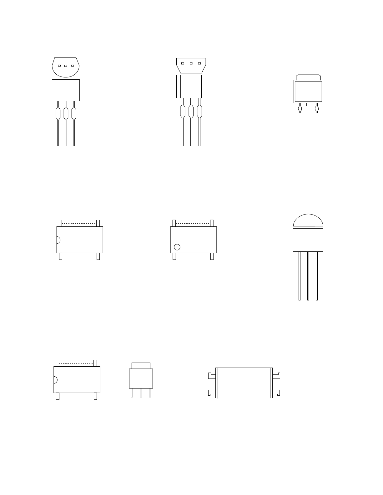
LEAD IDENTIFICATIONS
KTA1266(Y)
KTC3198(Y)
KTC3203(Y)
E C B E C B
KIA4558P/P
8
5
PT6313-S-TP(L)
28
KRA110M
KRC101M
KTA1267(Y)
KTC3199(GR)
15
2SK3498
GDS
KIA431-AT
1
MM1622XJBE
24
1
13
12
4
LD1117SC-R
123
1
1: GND
2: Vout
3: Vin
14
K A R
LTV-817B-F
A
K
C
E
Note:
A: Anode
K: Cathode
E: Emitter
C: Collector
B: Base
R: Reference
G: Gate
D: Drain
S: Source
1-14-1 E6121LE
Page 38
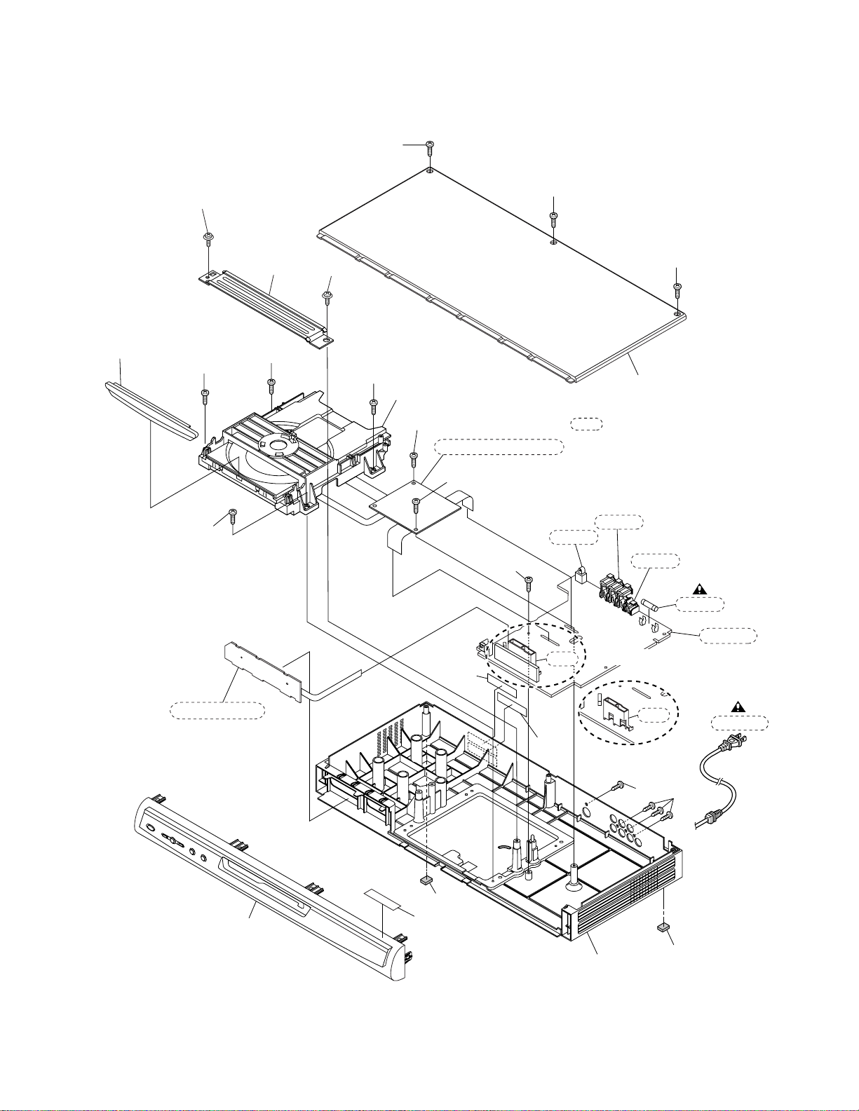
Cabinet
EXPLODED VIEWS
2L011
A2
2L081
2L021
2L021
2B5
2L021
2L081
2L021
1B1
2L105
DVD Main CBA Unit
2L105
2L031
2L011
2L011
A16
See Electrical Parts List
for parts with this mark.
Some Ref. Numbers are
not in sequence.
JK1404
JK1401
JK1202
Function CBA
A1X
A23
A13
A21
A22
2B1
[ DVL700F ]
2B1
[ DVL150F ]
2L041
A15
F1001
AV CBA
AC1001
2L041
A13
1-15-1 E6121CEX
Page 39
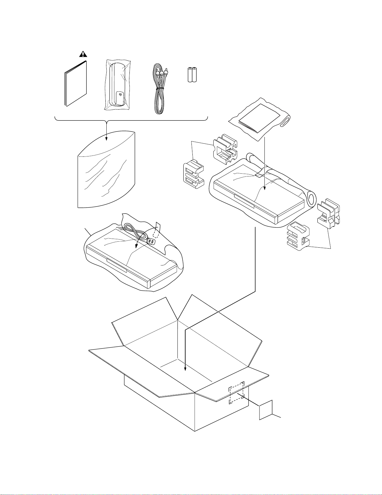
Packing
X10
X4
S4
X1
X5
X2
S2
Unit
S1
S2
A22
1-15-2 E6121PEX
Page 40
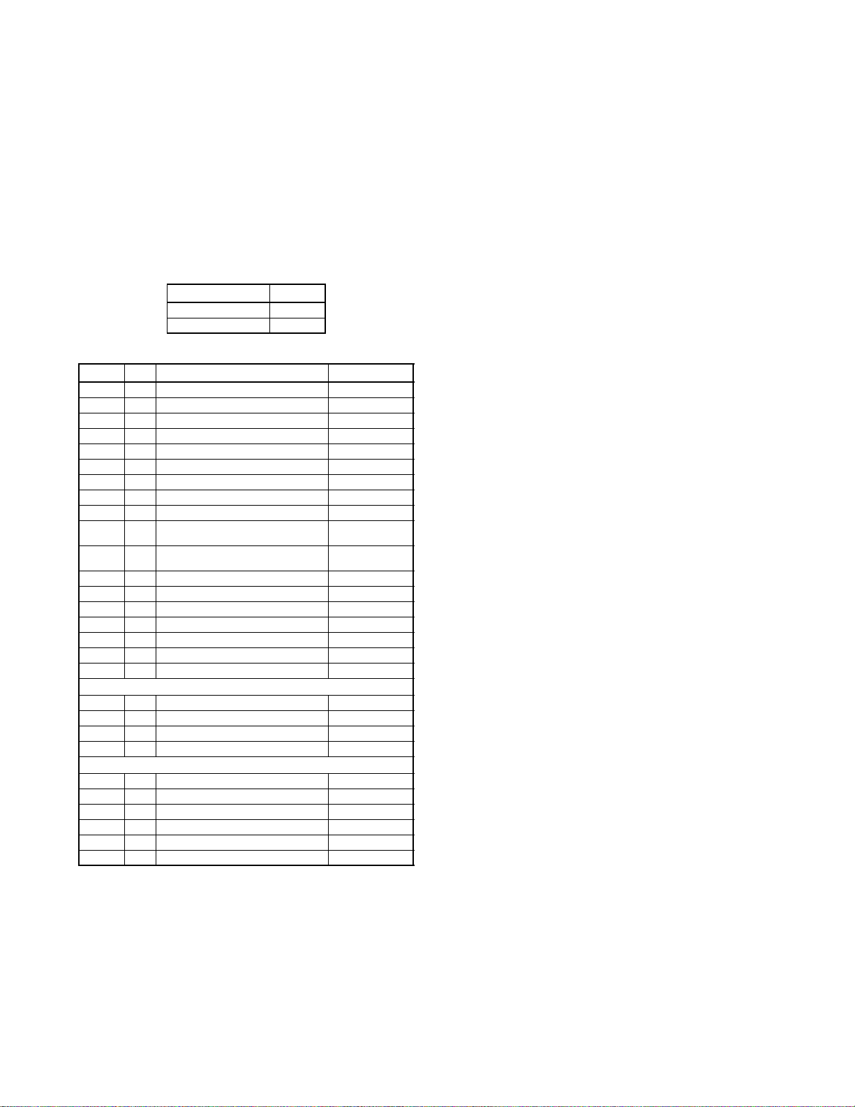
MECHANICAL PARTS LIST
PRODUCT SAFETY NOTE: Products marked with a
# have special characteristics important to safety.
Before replacing any of these components, read
carefully the product safety notice in this service
manual. Don't degrade the safety of the product
through improper servicing.
NOTE: Parts that are not assigned part numbers
(---------) are not available.
Comparison Chart of Models and Marks
Model Mark
DVL700F A
DVL150F B
Ref. No. Mark Description Part No.
A1X A FRONT ASSEMBLY E6121UD 1VM220368
A1X B FRONT ASSEMBLY E6122UD 1VM220375
A2 PANEL TRAY E5920UD 0VM204430
A13 FOOT(REAR) E5710UD 0VM415007
A15 CHASSIS(USA V2) E6170UD 1VM220323
A16 TOP CASE(V2) E6170UD 1VM320680
A21 A MODEL NO. LABEL E6121UD ---------A21 B MODEL NO. LABEL E6122UD ---------A22 LABEL BAR CODE E5900UD ---------A23 LABEL TELEPHONE NUMBER
1B1 DVD MECHA E6160(FG LESS)
2B5 REINFORCE PLATE E6160UD 1VM421017
2L011 SCREW P-TIGHT 3X10 BIND HEAD+ GBEP3100
2L021 SCREW P-TIGHT 3X11 BIND HEAD+ GBMP3110
2L031 P-TIGHT SCREW 3X8 BIND + GBMP3080
2L041 SCREW B-TIGHT M3X8 BIND HEAD + GBKB3080
2L081 SCREW P-TIGHT M3X8 WASHER+ GCMP3080
2L105 P-TIGHT SCREW 3X8 BIND + GBMP3080
H5730UD(SYLVANIA)
N79F0JVM
PACKING
S1 A GIFT BOX CARTON E6121UD 1VM320684
S1 B GIFT BOX CARTON E6122UD 1VM320730
S2 SIDE PAD E5900UD 0VM101344
S4 UNIT BAG E5500UD 0VM411683
ACCESSORIES
X1 REMOTE CONTROL UNIT E6121UD NB064UD
X2 DRY BATTERY R6P/2S XB0M451T0001
X4 ACCESSORY BAG E5700UD 0VM415576
X5 AV CORD TSCKA-Y/RW100 WPZ0102TM015
X10# A OWNERS MANUAL E6121UD 1VMN20407
X10# B OWNERS MANUAL E6122UD 1VMN20433
----------
N79F0JVM
20050222 1-16-1 E6121CA
Page 41
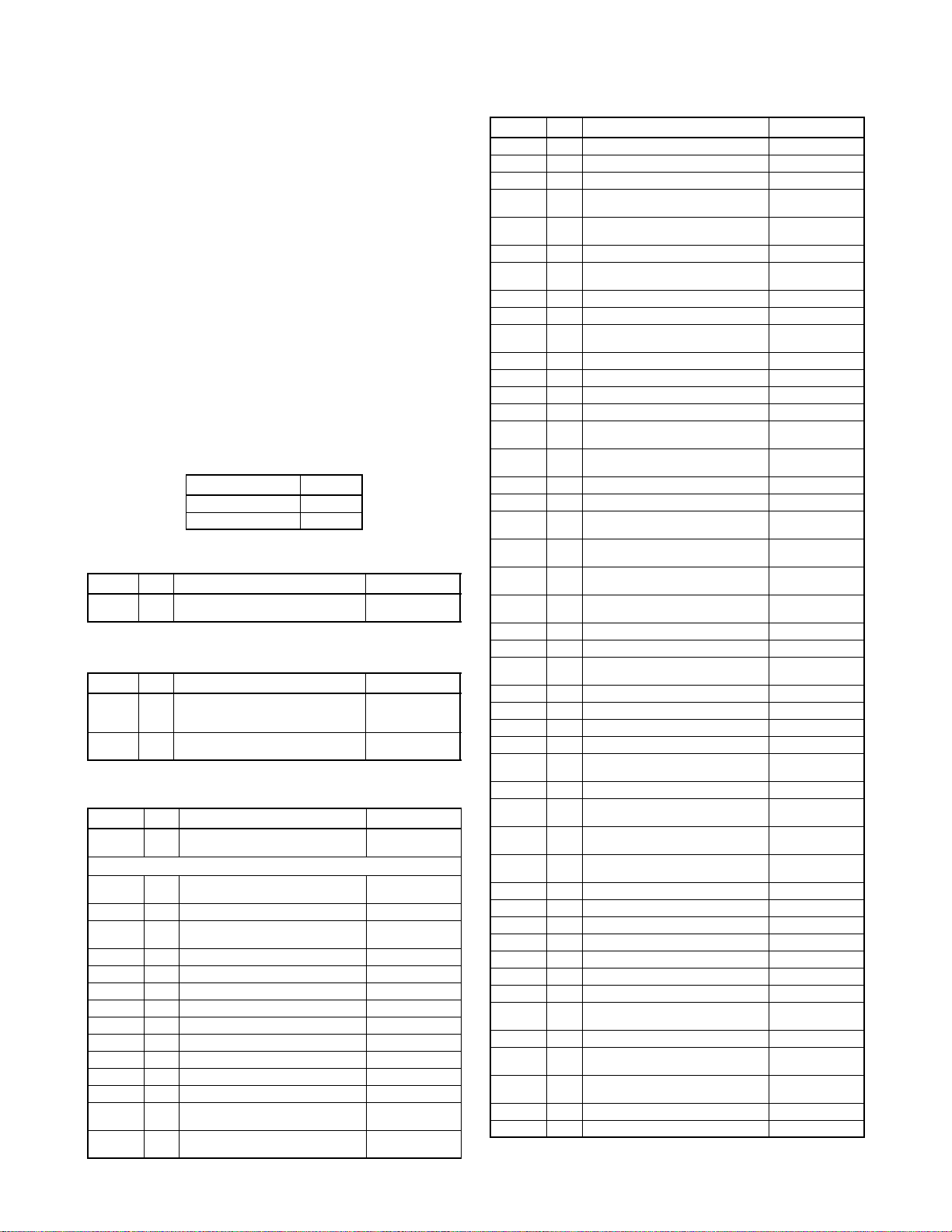
ELECTRICAL PARTS LIST
PRODUCT SAFETY NOTE: Products marked with a
# have special characteristics important to safety.
Before replacing any of these components, read
carefully the product safety notice in this service
manual. Don't degrade the safety of the product
through improper servicing.
NOTES:
1. Parts that are not assigned part numbers (---------)
are not available.
2. Tolerance of Capacitors and Resistors are noted
with the following symbols.
C.....±0.25% D.....±0.5% F.....±1%
G.....±2% J......±5% K.....±10%
M.....±20% N.....±30% Z.....+80/-20%
Comparison Chart of Models and Marks
Model Mark
DVL700F A
DVL150F B
DVD MAIN CBA UNIT
Ref. No. Mark Description Part No.
ABDVD MAIN CBA UNIT
DVD MAIN CBA UNIT
N79F2JUP
N79F4JUP
AV CBA ASSEMBLY
Ref. No. Mark Description Part No.
ABAV CBA ASSEMBLY
AV CBA ASSEMBLY
Consists of the following
AV C BA
FUNCTION CBA
AV CBA
Ref. No. Mark Description Part No.
AV CBA
Consists of the following:
CAPACITORS
C1001# METALLIZED FILM CAP. 0.047µF/ 250V MCT2E473MS037
C1003 ELECTROLYTIC CAP. 2.2µF/ 250V M CA2E2R2S6009
C1004 ELECTROLYTIC CAPACITOR
C1005 CERAMIC CAP. CH J 56pF/500V CCD2JJPCH560
C1006# SAFETY CAP. 2200pF/250V CCD2EMA0E222
C1007 ELECTROLYTIC CAP. 1000µF/ 6.3V M CE0KMASDL102
C1009 ELECTROLYTIC CAP. 1000µF/ 6.3V M CE0KMASDL102
C1010 CERAMIC CAP.(AX) CH J 680pF/50V CA1J681TU008
C1013 FILM CAP.(P) 0.0033µF/ 50V J CA1J332MS029
C1014 ELECTROLYTIC CAP. 1000µF/ 6.3V M CE0KMASDL102
C1017 CERAMIC CAP.(AX) Y M 0.01µF/ 16V CCA1CMT0Y103
C1018 ELECTROLYTIC CAP. 100µF/ 6.3V M CE0KMASDL101
C1021 CHIP CERAMIC CAP.(1608) B K 0.01µF/
C1022 CHIP CERAMIC CAP.(1608) B K 0.01µF/
ZR200TA820M12BB
50V
50V
1VSA11024
1VSA11106
----------
----------
----------
CA2D820DYG01
CHD1JK30B103
CHD1JK30B103
Ref. No. Mark Description Part No.
C1029 CERAMIC CAP.(AX) X K 2200pF/16V CCA1CKT0X222
C1034 ELECTROLYTIC CAP. 470µF/ 6.3V M CE0KMASDL471
C1035 ELECTROLYTIC CAP. 1000µF/ 16V M CE1CMASDL102
C1036 CHIP CERAMIC CAP.(1608) B K 0.01µF/
C1037 CHIP CERAMIC CAP.(1608) F Z 0.1µF/
C1038 ELECTROLYTIC CAP. 470µF/ 6.3V M CE0KMASDL471
C1039 CHIP CERAMIC CAP.(1608) F Z 0.1µF/
C1047 FILM CAP.(P) 0.01µF/ 100V J CA2A103MS029
C1048 ELECTROLYTIC CAP. 220µF/ 16V M CE1CMASDL221
C1049 A CHIP CERAMIC CAP.(1608) F Z 0.1µF/
C1201 ELECTROLYTIC CAP. 10µF/ 16V M CE1CMASDL100
C1202 ELECTROLYTIC CAP. 10µF/ 16V M CE1CMASDL100
C1205 CHIP CERAMIC CAP. CH J 220pF/50V CHD1JJ3CH221
C1206 CHIP CERAMIC CAP. CH J 220pF/50V CHD1JJ3CH221
C1207 CHIP CERAMIC CAP.(1608) CH J 47pF/
C1208 CHIP CERAMIC CAP.(1608) CH J 47pF/
C1221 ELECTROLYTIC CAP. 10µF/ 16V M H7 CE1CMASSL100
C1222 ELECTROLYTIC CAP. 10µF/ 16V M CE1CMASDL100
C1223 CHIP CERAMIC CAP.(1608) CH J
C1224 CHIP CERAMIC CAP.(1608) CH J
C1245 CHIP CERAMIC CAP.(1608) F Z 0.1µF/
C1246 CHIP CERAMIC CAP.(1608) F Z 0.1µF/
C1247 ELECTROLYTIC CAP. 470µF/ 6.3V M CE0KMASDL471
C1249 ELECTROLYTIC CAP. 47µF/ 16V M H7 CE1CMASSL470
C1351 CHIP CERAMIC CAP.(1608) B K 0.1µF/
C1352 ELECTROLYTIC CAP. 47µF/ 6.3V M H7 CE0KMASSL470
C1394 ELECTROLYTIC CAP. 47µF/ 10V M CE1AMASDL470
C1395 ELECTROLYTIC CAP. 1000µF/ 6.3V M CE0KMASDL102
C1396 CHIP RES.(1608) 1/10W 0 Ω RRXAZR5Z0000
C1397 CHIP CERAMIC CAP.(1608) F Z 0.1µF/
C1402 ELECTROLYTIC CAP. 470µF/ 6.3V M CE0KMASDL471
C1421 CHIP CERAMIC CAP.(1608) B K 0.01µF/
C1422 CHIP CERAMIC CAP.(1608) B K 0.1µF/
C1441 CHIP CERAMIC CAP.(1608) B K 0.33µF/
C1442 ELECTROLYTIC CAP. 1000µF/ 6.3V M CE0KMASDL102
C1461 ELECTROLYTIC CAP. 1µF/ 50V M CE1JMASDL010
C1462 ELECTROLYTIC CAP. 220µF/ 6.3V M CE0KMASDL221
C1481 ELECTROLYTIC CAP. 1µF/ 50V M CE1JMASDL010
C1482 ELECTROLYTIC CAP. 220µF/ 6.3V M CE0KMASDL221
C1522 ELECTROLYTIC CAP. 10µF/ 16V M CE1CMASDL100
C1524 ELECTROLYTIC CAP. 100µF/ 6.3V M CE0KMASDL101
C1531 CHIP CERAMIC CAP.(1608) B K 0.01µF/
C1532 ELECTROLYTIC CAP. 22µF/ 6.3V M H7 CE0KMASSL220
C1533 CHIP CERAMIC CAP.(1608) F Z 0.1µF/
C1534 CHIP CERAMIC CAP.(1608) F Z 0.1µF/
C2001 A ELECTROLYTIC CAP. 22µF/ 50V M CE1JMASDL220
C2002 A ELECTROLYTIC CAP. 22µF/ 50V M CE1JMASDL220
50V
50V
50V
50V
50V
50V
1000pF/50V
1000pF/50V
50V
50V
25V
50V
50V
25V
10V
50V
50V
50V
CHD1JK30B103
CHD1JZ30F104
CHD1JZ30F104
CHD1JZ30F104
CHD1JJ3CH470
CHD1JJ3CH470
CHD1JJ3CH102
CHD1JJ3CH102
CHD1JZ30F104
CHD1JZ30F104
CHD1EK30B104
CHD1JZ30F104
CHD1JK30B103
CHD1EK30B104
CHD1AK30B334
CHD1JK30B103
CHD1JZ30F104
CHD1JZ30F104
20050222 1-17-1 E6121EL
Page 42
Ref. No. Mark Description Part No.
C2003 CHIP CERAMIC CAP.(1608) F Z 0.1µF/
C2004 CHIP CERAMIC CAP.(1608) F Z 0.1µF/
C2031 ELECTROLYTIC CAP. 100µF/ 6.3V M CE0KMASDL101
C2032 CHIP CERAMIC CAP.(1608) F Z 0.1µF/
50V
50V
50V
CHD1JZ30F104
CHD1JZ30F104
CHD1JZ30F104
CONNECTORS
CN1001 22P FFC AV PCB TO MAIN WX1E5900-001
CN1601 FFC CABLE 17P AV PCB TO MAIN PCB WX1E6120-001
CN2001 FMN CONNECTOR TOP 6P 06FMN-
BTRK-A(LF)(SN)
JCFNG06JG020
DIODES
D1001 RECTIFIER DIODE 1N4005 NDQZ001N4005
D1002 RECTIFIER DIODE 1N4005 NDQZ001N4005
D1003 A RECTIFIER DIODE BA157 NDQZ000BA157
D1004 RECTIFIER DIODE 1N4005 NDQZ001N4005
D1005 RECTIFIER DIODE 1N4005 NDQZ001N4005
D1006 SCHOTTKY BARRIER DIODE SB140 NDQZ000SB140
D1008 SCHOTTKY BARRIER DIODE SB140 NDQZ000SB140
D1011 RECTIFIER DIODE BA157 NDQZ000BA157
D1012 SWITCHING DIODE 1N4148M NDTZ01N4148M
D1016 RECTIFIER DIODE BA157 NDQZ000BA157
D1017 ZENER DIODE DZ-18BSBT265 NDTB00DZ18BS
D1018 SWITCHING DIODE 1N4148M NDTZ01N4148M
D1024 SWITCHING DIODE 1N4148M NDTZ01N4148M
D1030 RECTIFIER DIODE FR202-B/P NDQZ000FR202
D1046 ZENER DIODE DZ-5.6BSCT265 NDTC0DZ5R6BS
D1047 ZENER DIODE DZ-5.1BSBT265 NDTB0DZ5R1BS
D1048 ZENER DIODE DZ-13BSBT265 NDTB00DZ13BS
D1053 PCB JUMPER D0.6-P10.0 JW10.0T
D1054 PCB JUMPER D0.6-P10.0 JW10.0T
D1055 A SWITCHING DIODE 1N4148M NDTZ01N4148M
D1058 SCHOTTKY BARRIER DIODE SB140 NDQZ000SB140
D1059 PCB JUMPER D0.6-P10.0 JW10.0T
D1073 PCB JUMPER D0.6-P5.0 JW5.0T
D1301 ZENER DIODE DZ-5.6BSBT265 NDTB0DZ5R6BS
D2021 B LED(GREEN) 204-10GD/S957 NPQZ10GDS957
D2022 B LED(GREEN) 204-10GD/S957 NPQZ10GDS957
D2023 B LED(RED) 204HD/E NPQZ00204HDE
D2041 A SWITCHING DIODE 1N4148M NDTZ01N4148M
D2041 B PCB JUMPER D0.6-P5.0 JW5.0T
D2042 A SWITCHING DIODE 1N4148M NDTZ01N4148M
D2042 B PCB JUMPER D0.6-P5.0 JW5.0T
D2043 A SWITCHING DIODE 1N4148M NDTZ01N4148M
D2043 B PCB JUMPER D0.6-P5.0 JW5.0T
D2044 A SWITCHING DIODE 1N4148M NDTZ01N4148M
D2044 B PCB JUMPER D0.6-P5.0 JW5.0T
D2045 ZENER DIODE DZ-6.2BSBT265 NDTB0DZ6R2BS
ICS
IC1001# PHOTOCOUPLER LTV-817B-F NPEB0LTV817F
IC1002 VOLTAGE REGULATOR LD1117SC-R NSZBA0TSS229
IC1006 IC SHUNT REGULATOR KIA431-AT NSZLA0TJY001
IC1201 IC OP AMP KIA4558P/P NSZBA0SJY035
IC1402 DRIVER FOR DVD MM1622XJBE QSZBA0TMM085
IC2001 VFD DRIVER/CONTROLLER IC
PT6313-S-TP(L)
NSZBA0TG2007
COILS
L1001# LINE FILTER 20MH SA-00911 LLBG00ZSA003
L1007 CHOKE COIL 47µH-K LLBD00PKV005
L1009 CHOKE COIL 47µH-K LLBD00PKV005
L1350 INDUCTOR(100µH K) LAP02TA101K LLAXKATTU101
L1351 INDUCTOR(0.47µH K) LAP02TAR47K LLAXKATTUR47
L1521 PCB JUMPER D0.6-P5.0 JW5.0T
Ref. No. Mark Description Part No.
L1522 CHIP RES.(1608) 1/10W 0 Ω RRXAZR5Z0000
L2020 B PCB JUMPER D0.6-P5.0 JW5.0T
L2031 INDUCTOR(100µH K) LAP02TA101K LLAXKATTU101
TRANSISTORS
Q1002 TRANSISTOR KTA1267(Y) NQSY0KTA1267
Q1003 TRANSISTOR KTC3199(GR) NQS10KTC3199
Q1004 TRANSISTOR KTC3198(Y) NQSY0KTC3198
Q1005 A TRANSISTOR KTC3199(GR) NQS10KTC3199
Q1011 TRANSISTOR KTC3203(Y) NQSY0KTC3203
Q1015 A RES. BUILT-IN TRANSISTOR KRA110M NQSZ0KRA110M
Q1016 TRANSISTOR KTC3199(GR) NQS10KTC3199
Q1031# FET 2SK3498(T6L1FUNANQ) QF1Z02SK3498
Q1201 TRANSISTOR KTC3199(GR) NQS10KTC3199
Q1202 TRANSISTOR KTC3199(GR) NQS10KTC3199
Q1204 TRANSISTOR KTA1266(Y) NQSY0KTA1266
Q1351 TRANSISTOR KTC3199(GR) NQS10KTC3199
Q1352 TRANSISTOR KTC3199(GR) NQS10KTC3199
Q2021 B RES. BUILT-IN TRANSISTOR KRC101M NQSZ0KRC101M
Q2022 B RES. BUILT-IN TRANSISTOR KRC101M NQSZ0KRC101M
RESISTORS
R1002 A PCB JUMPER D0.6-P5.0 JW5.0T
R1004 METAL OXIDE FILM RES. 1W J 82k Ω RN01823ZU001
R1005 CARBON RES. 1/4W J 2.7M Ω RCX4JATZ0275
R1006 CARBON RES. 1/4W J 2.7M Ω RCX4JATZ0275
R1008 CARBON RES. 1/4W J 620 Ω RCX4JATZ0621
R1010 CARBON RES. 1/6W J 15k Ω RCX6JATZ0153
R1011 METAL OXIDE FILM RES. 1W J 1.2 Ω RN011R2ZU001
R1015 CARBON RES. 1/6W J 560 Ω RCX6JATZ0561
R1016 CARBON RES. 1/6W J 22k Ω RCX6JATZ0223
R1019 CHIP RES.(1608) 1/16W F 680 Ω RRXGFR5Z0681
R1020 CHIP RES.(1608) 1/10W J 1.2k Ω RRXAJR5Z0122
R1021 CHIP RES.(1608) 1/10W J 2.7k Ω RRXAJR5Z0272
R1022 CHIP RES.(1608) 1/10W J 820 Ω RRXAJR5Z0821
R1023 CHIP RES.(1608) 1/16W F 2.2k Ω RRXGFR5Z0222
R1025 CHIP RES.(1608) 1/10W J 10k Ω RRXAJR5Z0103
R1029 CARBON RES. 1/6W J 470k Ω RCX6JATZ0474
R1032 CARBON RES. 1/6W J 3.3k Ω RCX6JATZ0332
R1035 CARBON RES. 1/4W J 1k Ω RCX4JATZ0102
R1043 METAL OXIDE FILM RES. 1W J 2.7 Ω RN012R7ZU001
R1044 CHIP RES.(1608) 1/10W J 100k Ω RRXAJR5Z0104
R1059 CHIP RES.(1608) 1/10W J 10k Ω RRXAJR5Z0103
R1061 A CARBON RES. 1/6W J 1.2k Ω RCX6JATZ0122
R1062 A CARBON RES. 1/6W J 1.2k Ω RCX6JATZ0122
R1067 CHIP RES.(1608) 1/10W J 1k Ω RRXAJR5Z0102
R1068 CHIP RES.(1608) 1/10W J 560 Ω RRXAJR5Z0561
R1069 CARBON RES. 1/6W J 560 Ω RCX6JATZ0561
R1072 CHIP RES.(1608) 1/10W J 330 Ω RRXAJR5Z0331
R1073 METAL OXIDE FILM RES. 2W J 33 Ω RN02330ZU001
R1074 RECTIFIER DIODE 1N4005 NDQZ001N4005
R1075 CHIP RES. 1/16W F 10 Ω RRXGFR5Z0100
R1076 CHIP RES. 1/16W F 1k Ω RRXGFR5Z0102
R1078 A CARBON RES. 1/4W J 680 Ω RCX4JATZ0681
R1079 CARBON RES. 1/4W J 2.2 Ω RCX4JATZ02R2
R1080 CHIP RES.(1608) 1/10W J 22k Ω RRXAJR5Z0223
R1081 CHIP REG. 1/16W F 100 Ω RRXGFR5Z0101
R1083 A PCB JUMPER D0.6-P5.0 JW5.0T
R1084 A CHIP RES.(1608) 1/10W J 220k Ω RRXAJR5Z0224
R1085 A CHIP RES.(1608) 1/10W J 6.8k Ω RRXAJR5Z0682
R1086 CHIP RES.(1608) 1/10W 0 Ω RRXAZR5Z0000
R1091 CHIP RES.(1608) 1/10W 0 Ω RRXAZR5Z0000
R1095 CHIP RES.(2125) 1/8W J 0.1 Ω RRX8R10HH005
R1205 CHIP RES.(1608) 1/16W F 20k Ω RRXGFR5Z0203
20050222 1-17-2 E6121EL
Page 43
Ref. No. Mark Description Part No.
R1206 CHIP RES.(1608) 1/16W F 20k Ω RRXGFR5Z0203
R1207 CHIP RES.(1608) 1/10W J 8.2k Ω RRXAJR5Z0822
R1208 CHIP RES.(1608) 1/10W J 8.2k Ω RRXAJR5Z0822
R1209 CHIP RES. 1/16W F 30k Ω RRXGFR5Z0303
R1210 CHIP RES. 1/16W F 30k Ω RRXGFR5Z0303
R1221 CHIP RES.(1608) 1/10W J 100k Ω RRXAJR5Z0104
R1222 CHIP RES.(1608) 1/10W J 100k Ω RRXAJR5Z0104
R1223 CHIP RES.(1608) 1/10W J 470 Ω RRXAJR5Z0471
R1224 CHIP RES.(1608) 1/10W J 470 Ω RRXAJR5Z0471
R1225 CHIP RES.(1608) 1/10W J 1k Ω RRXAJR5Z0102
R1226 CHIP RES.(1608) 1/10W J 1k Ω RRXAJR5Z0102
R1227 CHIP RES.(1608) 1/10W J 220 Ω RRXAJR5Z0221
R1228 CHIP RES.(1608) 1/10W J 220 Ω RRXAJR5Z0221
R1240 CHIP RES.(1608) 1/10W J 100k Ω RRXAJR5Z0104
R1245 CHIP RES.(1608) 1/10W J 10 Ω RRXAJR5Z0100
R1351 CHIP RES.(1608) 1/10W J 2k Ω RRXAJR5Z0202
R1352 CHIP RES.(1608) 1/10W J 2.2k Ω RRXAJR5Z0222
R1353 CHIP RES.(1608) 1/10W J 2.2k Ω RRXAJR5Z0222
R1354 CHIP RES.(1608) 1/10W J 220 Ω RRXAJR5Z0221
R1355 CHIP RES.(1608) 1/10W J 75 Ω RRXAJR5Z0750
R1356 CHIP RES.(1608) 1/10W J 100k Ω RRXAJR5Z0104
R1392 CHIP RES.(1608) 1/10W J 1k Ω RRXAJR5Z0102
R1396 CHIP RES.(1608) 1/10W J 470 Ω RRXAJR5Z0471
R1397 CHIP RES.(1608) 1/10W J 470 Ω RRXAJR5Z0471
R1402 CHIP RES.(1608) 1/10W J 75 Ω RRXAJR5Z0750
R1421 CHIP RES. 1/16W F 160 Ω RRXGFR5Z0161
R1422 CHIP RES.(1608) 1/10W J 75 Ω RRXAJR5Z0750
R1441 CHIP RES. 1/16W F 160 Ω RRXGFR5Z0161
R1442 CHIP RES.(1608) 1/10W J 75 Ω RRXAJR5Z0750
R1443 CHIP RES.(1608) 1/10W J 75 Ω RRXAJR5Z0750
R1461 CHIP RES. 1/16W F 75 Ω RRXGFR5Z0750
R1462 CHIP RES.(1608) 1/10W J 75 Ω RRXAJR5Z0750
R1481 CHIP RES. 1/16W F 75 Ω RRXGFR5Z0750
R1482 CHIP RES.(1608) 1/10W J 75 Ω RRXAJR5Z0750
R1613 CHIP RES.(1608) 1/10W 0 Ω RRXAZR5Z0000
R2001 CARBON RES. 1/6W J 10 Ω RCX6JATZ0100
R2002 CHIP RES.(1608) 1/10W J 68k Ω RRXAJR5Z0683
R2012 CHIP RES.(1608) 1/10W J 1k Ω RRXAJR5Z0102
R2013 CHIP RES.(1608) 1/10W J 1k Ω RRXAJR5Z0102
R2014 CHIP RES.(1608) 1/10W J 1k Ω RRXAJR5Z0102
R2015 CHIP RES.(1608) 1/10W J 1k Ω RRXAJR5Z0102
R2016 CHIP RES.(1608) 1/10W J 10k Ω RRXAJR5Z0103
R2021 B CARBON RES. 1/6W J 220 Ω RCX6JATZ0221
R2022 B CARBON RES. 1/6W J 220 Ω RCX6JATZ0221
R2023 B CARBON RES. 1/6W J 150 Ω RCX6JATZ0151
R2031 CHIP RES.(1608) 1/10W J 6.8k Ω RRXAJR5Z0682
R2032 CHIP RES.(1608) 1/10W J 10k Ω RRXAJR5Z0103
R2033 CHIP RES.(1608) 1/10W J 22k Ω RRXAJR5Z0223
R2041 CHIP RES.(1608) 1/10W J 10k Ω RRXAJR5Z0103
R2042 CHIP RES.(1608) 1/10W J 10k Ω RRXAJR5Z0103
R2043 CHIP RES.(1608) 1/10W J 10k Ω RRXAJR5Z0103
R2044 CHIP RES.(1608) 1/10W J 10k Ω RRXAJR5Z0103
MISCELLANEOUS
2B1 HOLDER F.I.P. E5900UD 0VM416070
AC1001# AC CORD PB8B2F9110A-055 WAC0162LW004
F1001# FUSE SIC 1A 250V U/C PSE PAGG20CW3102
FL2001 A V.F.D. 7-BT-298NYM TVFD150FT014
FH1001 FUSE HOLDER MSF-015 XH01Z00LY001
FH1002 FUSE HOLDER MSF-015 XH01Z00LY001
J2009 B CARBON RES. 1/6W J 10k Ω RCX6JATZ0103
J2647 CERAMIC CAP.(AX) CH J 680pF/50V CA1J681TU008
JK1202 RCA JACK(BLACK) MSP-251V-01 NI JXRL010LY070
Ref. No. Mark Description Part No.
JK1401 S TYPE JACK MDC-050V-2.4 JXEL040LY001
JK1404 RCA JACK MSD-246V-65NI/PBSN JXRL060LY069
RM2001 REMOTE RECEIVER MIM-93M6DKF USESJRSUNT01
T1001# PULSE TRANS CGS-SW0078A LTT00CPSA175
FUNCTION CBA
Ref. No. Description Part No.
FUNCTION CBA
Consists of the following:
CONNECTOR
CN2101 6P FFC AV PCB TO SW PCB WX1E5900-005
SWITCHES
SW2101 TACT SWITCH KSM0614B SST0101HH013
SW2104 TACT SWITCH KSM0614B SST0101HH013
SW2105 TACT SWITCH KSM0614B SST0101HH013
SW2106 TACT SWITCH KSM0614B SST0101HH013
SW2107 TACT SWITCH KSM0614B SST0101HH013
SW2108 TACT SWITCH KSM0614B SST0101HH013
----------
20050222 1-17-3 E6121EL
Page 44

DVL700F/DVL150F
E6121UD/E6122UD
2005-03-22
 Loading...