

SERVICE MANUAL
20″ LCD TV/DVD
6620LDF

IMPORTANT SAFETY NOTICE
Proper service and repair is important to the safe, reliable operation of all
Funai Equipment. The service procedures recommended by Funai and
described in this service manual are effective methods of performing
service operations. Some of these service special tools should be used
when and as recommended.
It is important to note that this service manual contains various CAUTIONS
and NOTICES which should be carefully read in order to minimize the risk
of personal injury to service personnel. The possibility exists that improper
service methods may damage the equipment. It also is important to
understand that these CAUTIONS and NOTICES ARE NOT EXHAUSTIVE.
Funai could not possibly know, evaluate and advice the service trade of all
conceivable ways in which service might be done or of the possible
hazardous consequences of each way. Consequently, Funai has not
undertaken any such broad evaluation. Accordingly, a servicer who uses a
service procedure or tool which is not recommended by Funai must first
use all precautions thoroughly so that neither his safety nor the safe
operation of the equipment will be jeopardized by the service method
selected.
The LCD panel is manufactured to provide many years of useful life.
Occasionally a few non active pixels may appear as a tiny spec of color.
This is not to be considered a defect in the LCD screen.
Manufactured under license from Dolby Laboratories.
“Dolby” and the double-D symbol are trademarks of Dolby Laboratories.

TABLE OF CONTENTS
Specifications . . . . . . . . . . . . . . . . . . . . . . . . . . . . . . . . . . . . . . . . . . . . . . . . . . . . . . . . . . . . . . . . . . . . . . . . . . . 1-1
Laser Beam Safety Precautions . . . . . . . . . . . . . . . . . . . . . . . . . . . . . . . . . . . . . . . . . . . . . . . . . . . . . . . . . . . . . 2-1
Important Safety Precautions . . . . . . . . . . . . . . . . . . . . . . . . . . . . . . . . . . . . . . . . . . . . . . . . . . . . . . . . . . . . . . . 3-1
Standard Notes for Servicing . . . . . . . . . . . . . . . . . . . . . . . . . . . . . . . . . . . . . . . . . . . . . . . . . . . . . . . . . . . . . . . 4-1
Cabinet Disassembly Instructions. . . . . . . . . . . . . . . . . . . . . . . . . . . . . . . . . . . . . . . . . . . . . . . . . . . . . . . . . . . . 5-1
Electrical Adjustment Instructions . . . . . . . . . . . . . . . . . . . . . . . . . . . . . . . . . . . . . . . . . . . . . . . . . . . . . . . . . . . . 6-1
How to Initialize the LCD TV/DVD. . . . . . . . . . . . . . . . . . . . . . . . . . . . . . . . . . . . . . . . . . . . . . . . . . . . . . . . . . . . 7-1
Firmware Renewal Mode . . . . . . . . . . . . . . . . . . . . . . . . . . . . . . . . . . . . . . . . . . . . . . . . . . . . . . . . . . . . . . . . . . 8-1
Block Diagrams . . . . . . . . . . . . . . . . . . . . . . . . . . . . . . . . . . . . . . . . . . . . . . . . . . . . . . . . . . . . . . . . . . . . . . . . . . 9-1
Schematic Diagrams / CBA's and Test Points. . . . . . . . . . . . . . . . . . . . . . . . . . . . . . . . . . . . . . . . . . . . . . . . . . 10-1
Waveforms . . . . . . . . . . . . . . . . . . . . . . . . . . . . . . . . . . . . . . . . . . . . . . . . . . . . . . . . . . . . . . . . . . . . . . . . . . . . 11-1
Wiring Diagram . . . . . . . . . . . . . . . . . . . . . . . . . . . . . . . . . . . . . . . . . . . . . . . . . . . . . . . . . . . . . . . . . . . . . . . . . 12-1
System Control Timing Charts . . . . . . . . . . . . . . . . . . . . . . . . . . . . . . . . . . . . . . . . . . . . . . . . . . . . . . . . . . . . . 13-1
Lead Identifications . . . . . . . . . . . . . . . . . . . . . . . . . . . . . . . . . . . . . . . . . . . . . . . . . . . . . . . . . . . . . . . . . . . . . . 14-1
Exploded Views. . . . . . . . . . . . . . . . . . . . . . . . . . . . . . . . . . . . . . . . . . . . . . . . . . . . . . . . . . . . . . . . . . . . . . . . . 15-1
Mechanical Parts List . . . . . . . . . . . . . . . . . . . . . . . . . . . . . . . . . . . . . . . . . . . . . . . . . . . . . . . . . . . . . . . . . . . . 16-1
Electrical Parts List . . . . . . . . . . . . . . . . . . . . . . . . . . . . . . . . . . . . . . . . . . . . . . . . . . . . . . . . . . . . . . . . . . . . . . 17-1
SPECIFICATIONS
< LCD TV Section >
< TUNER >
ANT. Input ---------------------- 75 ohm Unbal., F type
Reference Level--------------- 20 Vp-p (LCD Green Cathode)
Test Input Signal -------------- 400 Hz 30% modulation
Description Condition Unit Nominal Limit
1. Intermediate Freq.
2. Color Killer Sens. CH-4 dBµV20 25
3. AFT Pull In Range (10 mV input) --- MHz ±2.1 ±0.7
Picture
Sound
MHz
MHz
45.75
41.25
---
---
< LCD PANEL >
Description Condition Unit Nominal Limit
1. Number of Pixels
2. Brightness cd/m
3. Response Time --- msec 16 ---
4. Support Color --- - 16 mil. (8 bit) ---
5. Viewing Angle
Horizontal
Vert ical
Horizontal
Vert ical
pixels
pixels
°
°
640 × 3
480
2
450 ---
-85 to 85
-80 to 85
---
---
---
---
< VIDEO >
Description Condition Unit Nominal Limit
1. Over Scan
Horizontal
Vert ical
%
%
5
5
---
---
2. Color Temperature
3. Resolution
--x
y
Horizontal
Vert ical
°K
line
line
9200
0.286
0.294
400
350
--±0.3
±0.3
---
---
< AUDIO >
All items are measured across 8 Ω load at speaker output terminal with L.P.F.
Description Condition Unit Nominal Limit
1. Audio Output Power 10% THD: Lch/Rch W 1.0/1.0 0.8/0.8
2. Audio Distortion 500mW: Lch/Rch % 1.0/1.0 4.0/4.0
-
3. Audio Freq. Response
Note: Nominal specifications represent the design specifications. All units should be able to approximate these.
Some will exceed and some may drop slightly below these specifications. Limit specifications represent
the absolute worst condition that still might be considered acceptable. In no case should a unit fail to meet
limit specifications.
3dB: Lch
-
3dB: Rch
Hz
Hz
50 to 12 k
50 to 12 k
---
---
1-1 L3250SP

<DVD Section>
ITEM CONDITIONS UNIT NOMINAL LIMIT
1. Coaxial Digital Out 75 ohm load mVpp 500 ± 100
NOTES:
1. All Items are measured without pre-emphasis unless otherwise specified.
2. Power supply : AC120 V 60 Hz
3. Ambient temperature: +25
°C
1-2 L3250SP
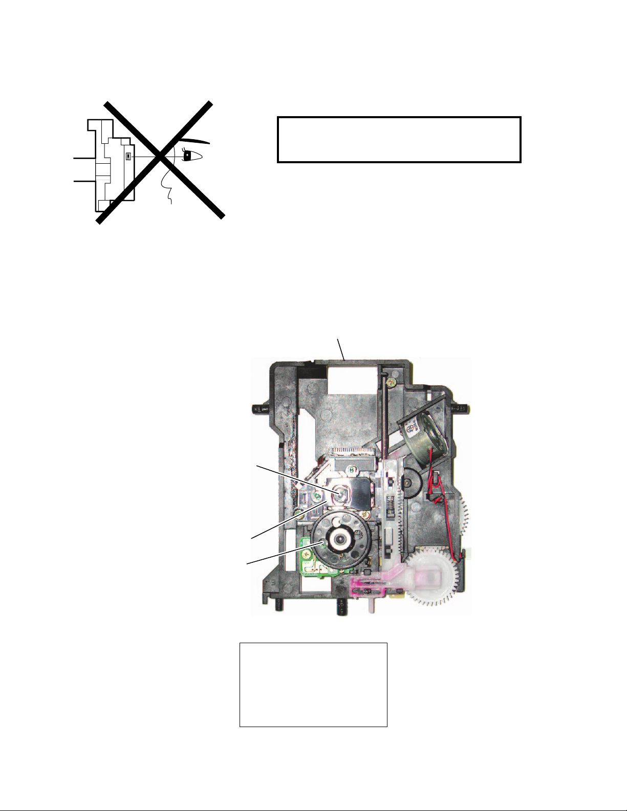
LASER BEAM SAFETY PRECAUTIONS
This DVD player uses a pickup that emits a laser beam.
Do not look directly at the laser beam coming
from the pickup or allow it to strike against your
skin.
The laser beam is emitted from the location shown in the figure. When checking the laser diode, be sure to keep
your eyes at least 30 cm away from the pickup lens when the diode is turned on. Do not look directly at the laser
beam.
CAUTION: Use of controls and adjustments, or doing procedures other than those specified herein, may result in
hazardous radiation exposure.
Drive Mechanism Assembly (within the DVD Mechanism)
Laser Beam Radiation
Laser Pickup
Turntable
WHEN OPEN. DO NOT
Location: Top of DVD mechanism.
CAUTION
LASER RADIATION
STARE INTO BEAM.
2-1 E6NLSP
IMPORTANT SAFETY PRECAUTIONS
Prior to shipment from the factory, our products are strictly inspected for recognized product safety and electrical
codes of the countries in which they are to be sold. However, in order to maintain such compliance, it is equally
important to implement the following precautions when a set is being serviced.
Safety Precautions for LCD TV
Circuit
1. Before returning an instrument to the
customer, always make a safety check of the
entire instrument, including, but not limited to, the
following items:
a. Be sure that no built-in protective devices are
defective and have been defeated during
servicing. (1) Protective shields are provided
on this chassis to protect both the technician
and the customer. Correctly replace all missing
protective shields, including any removed for
servicing convenience. (2) When reinstalling
the chassis and/or other assembly in the
cabinet, be sure to put back in place all
protective devices, including but not limited to,
nonmetallic control knobs, insulating
fishpapers, adjustment and compartment
covers/shields, and isolation resistor/capacitor
networks. Do not operate this instrument or
permit it to be operated without all
protective devices correctly installed and
functioning. Servicers who defeat safety
features or fail to perform safety checks
may be liable for any resulting damage.
b. Be sure that there are no cabinet openings
through which an adult or child might be able to
insert their fingers and contact a hazardous
voltage. Such openings include, but are not
limited to, (1) spacing between the Liquid
Crystal Panel and the cabinet mask, (2)
excessively wide cabinet ventilation slots, and
(3) an improperly fitted and/or incorrectly
secured cabinet back cover.
c. Antenna Cold Check - With the instrument AC
plug removed from any AC source, connect an
electrical jumper across the two AC plug
prongs. Place the instrument AC switch in the
on position. Connect one lead of an ohmmeter
to the AC plug prongs tied together and touch
the other ohmmeter lead in turn to each tuner
antenna input exposed terminal screw and, if
applicable, to the coaxial connector. If the
measured resistance is less than 1.0 megohm
or greater than 5.2 megohm, an abnormality
exists that must be corrected before the
instrument is returned to the customer. Repeat
this test with the instrument AC switch in the off
position.
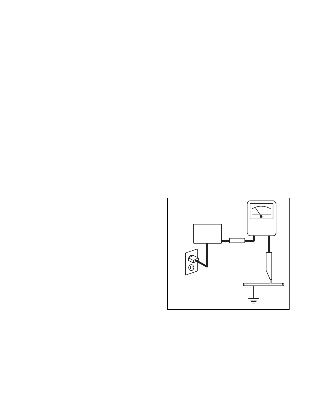
d. Leakage Current Hot Check - With the
instrument completely reassembled, plug the
AC line cord directly into a 120 V AC outlet. (Do
not use an isolation transformer during this
test.) Use a leakage current tester or a
metering system that complies with American
National Standards Institute (ANSI) C101.1
Leakage Current for Appliances and
Underwriters Laboratories (UL) 1410, (50.7).
With the instrument AC switch first in the on
position and then in the off position, measure
from a known earth ground (metal water pipe,
conduit, etc.) to all exposed metal parts of the
instrument (antennas, handle brackets, metal
cabinet, screw heads, metallic overlays, control
shafts, etc.), especially any exposed metal
parts that offer an electrical return path to the
chassis. Any current measured must not
exceed 0.5 milli-ampere. Reverse the
instrument power cord plug in the outlet and
repeat the test.
READING SHOULD
NOT BE ABOVE 0.5 mA
LEAKAGE
DEVICE
BEING
TESTED
TEST ALL EXPOSED
METAL SURFACES
ALSO TEST WITH
PLUG REVERSED
USING AC
ADAPTER PLUG
AS REQUIRED
ANY MEASUREMENTS NOT WITHIN THE
LIMITS SPECIFIED HEREIN INDICATE A
POTENTIAL SHOCK HAZARD THAT MUST
BE ELIMINATED BEFORE RETURNING THE
INSTRUMENT TO THE CUSTOMER OR
BEFORE CONNECTING THE ANTENNA OR
ACCESSORIES.
2. Read and comply with all caution and safety-
related notes on or inside the receiver cabinet, on
the receiver chassis, or on the Liquid Crystal
Panel.
CURRENT
TESTER
+
EARTH
GROUND
_
3-1 LTVN_ISP

3. Design Alteration Warning - Do not alter or add
to the mechanical or electrical design of this TV
receiver. Design alterations and additions,
including, but not limited to circuit modifications
and the addition of items such as auxiliary audio
and/or video output connections, might alter the
safety characteristics of this receiver and create a
hazard to the user. Any design alterations or
additions will void the manufacturer's warranty and
may make you, the servicer, responsible for
personal injury or property damage resulting
therefrom.
4. Hot Chassis Warning a. Some TV receiver chassis are electrically
connected directly to one conductor of the AC
power cord and maybe safety-serviced without
an isolation transformer only if the AC power
plug is inserted so that the chassis is
connected to the ground side of the AC power
source. To confirm that the AC power plug is
inserted correctly, with an AC voltmeter,
measure between the chassis and a known
earth ground. If a voltage reading in excess of
1.0V is obtained, remove and reinsert the AC
power plug in the opposite polarity and again
measure the voltage potential between the
chassis and a known earth ground.
b. Some TV receiver chassis normally have 85V
AC(RMS) between chassis and earth ground
regardless of the AC plug polarity. This chassis
can be safety-serviced only with an isolation
transformer inserted in the power line between
the receiver and the AC power source, for both
personnel and test equipment protection.
c. Some TV receiver chassis have a secondary
ground system in addition to the main chassis
ground. This secondary ground system is not
isolated from the AC power line. The two
ground systems are electrically separated by
insulation material that must not be defeated or
altered.
5. Observe original lead dress. Take extra care to
assure correct lead dress in the following areas: a.
near sharp edges, b. near thermally hot parts-be
sure that leads and components do not touch
thermally hot parts, c. the AC supply, d. high
voltage, and, e. antenna wiring. Always inspect in
all areas for pinched, out of place, or frayed wiring.
Check AC power cord for damage.
6. Components, parts, and/or wiring that appear to
have overheated or are otherwise damaged
should be replaced with components, parts, or
wiring that meet original specifications.
Additionally, determine the cause of overheating
and/or damage and, if necessary, take corrective
action to remove any potential safety hazard.
7. Product Safety Notice - Some electrical and
mechanical parts have special safety-related
characteristics which are often not evident from
visual inspection, nor can the protection they give
necessarily be obtained by replacing them with
components rated for higher voltage, wattage, etc..
Parts that have special safety characteristics are
identified by a # on schematics and in parts lists.
Use of a substitute replacement that does not
have the same safety characteristics as the
recommended replacement part might create
shock, fire, and/or other hazards. The product's
safety is under review continuously and new
instructions are issued whenever appropriate.
Prior to shipment from the factory, our products
are strictly inspected to confirm they comply with
the recognized product safety and electrical codes
of the countries in which they are to be sold.
However, in order to maintain such compliance, it
is equally important to implement the following
precautions when a set is being serviced.
3-2 LTVN_ISP

Precautions during Servicing
A. Parts identified by the # symbol are critical for
safety.
Replace only with part number specified.
B. In addition to safety, other parts and assemblies
are specified for conformance with regulations
applying to spurious radiation. These must also be
replaced only with specified replacements.
Examples: RF converters, RF cables, noise
blocking capacitors, and noise blocking filters, etc.
C. Use specified internal wiring. Note especially:
1) Wires covered with PVC tubing
2) Double insulated wires
3) High voltage leads
D. Use specified insulating materials for hazardous
live parts. Note especially:
1) Insulation Tape
2) PVC tubing
3) Spacers
4) Insulators for transistors.
E. When replacing AC primary side components
(transformers, power cord, etc.), wrap ends of
wires securely about the terminals before
soldering.
F. Observe that the wires do not contact heat
producing parts (heat sinks, oxide metal film
resistors, fusible resistors, etc.)
G. Check that replaced wires do not contact sharp
edged or pointed parts.
H. When a power cord has been replaced, check that
5~6 kg of force in any direction will not loosen it.
I. Also check areas surrounding repaired locations.
J. Use care that foreign objects (screws, solder
droplets, etc.) do not remain inside the set.
K. Crimp type wire connector
The power transformer uses crimp type
connectors which connect the power cord and the
primary side of the transformer. When replacing
the transformer, follow these steps carefully and
precisely to prevent shock hazards.
Replacement procedure
1) Remove the old connector by cutting the wires
at a point close to the connector.
Important: Do not re-use a connector (discard
it).
2) Strip about 15 mm of the insulation from the
ends of the wires. If the wires are stranded,
twist the strands to avoid frayed conductors.
3) Align the lengths of the wires to be connected.
Insert the wires fully into the connector.
4) Use the crimping tool to crimp the metal sleeve
at the center position. Be sure to crimp fully to
the complete closure of the tool.
L. When connecting or disconnecting the internal
connectors, first, disconnect the AC plug from the
AC supply outlet.
M. When installing parts or assembling the cabinet
parts, be sure to use the proper screws and
tighten certainly.
3-3 LTVN_ISP
Safety Check after Servicing
Examine the area surrounding the repaired location for damage or deterioration. Observe that screws, parts and
wires have been returned to original positions. Afterwards, perform the following tests and confirm the specified
values in order to verify compliance with safety standards.
1. Clearance Distance
When replacing primary circuit components, confirm
specified clearance distance (d) and (d') between
soldered terminals, and between terminals and
surrounding metallic parts. (See Fig. 1)
Table 1: Ratings for selected area
Chassis or Secondary Conductor
Primary Circuit Terminals
AC Line Voltage Region
110 to 130 V
Note: This table is unofficial and for reference only. Be
sure to confirm the precise values.
U.S.A. or
Canada
Clearance
Distance (d), (d’)
≥ 3.2 mm
(0.126 inches)
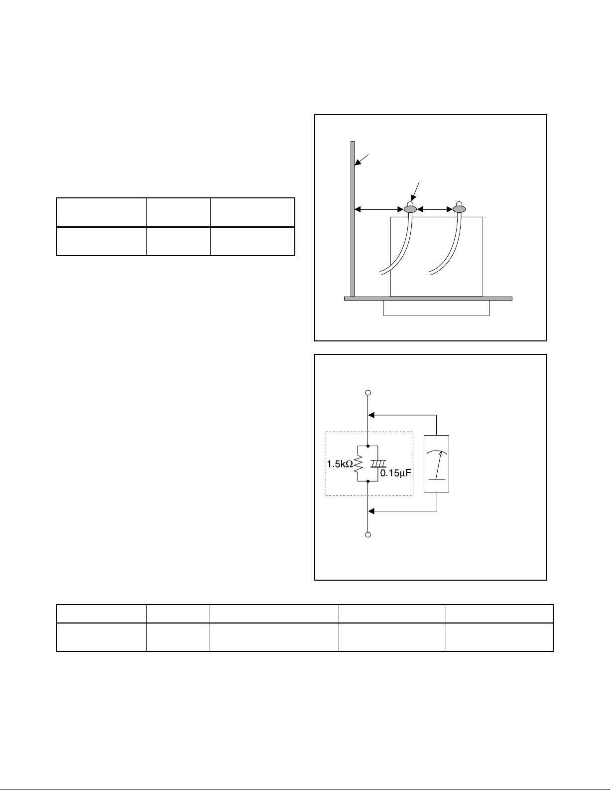
2. Leakage Current Test
Confirm the specified (or lower) leakage current
between B (earth ground, power cord plug prongs) and
externally exposed accessible parts (RF terminals,
antenna terminals, video and audio input and output
terminals, microphone jacks, earphone jacks, etc.) is
lower than or equal to the specified value in the table
below.
Measuring Method: (Power ON)
Insert load Z between B (earth ground, power cord plug
prongs) and exposed accessible parts. Use an AC
voltmeter to measure across both terminals of load Z.
See Fig. 2 and following table.
dd'
Fig. 1
Exposed Accessible Part
Z
AC Voltmeter
(High Impedance)
Earth Ground
B
Power Cord Plug Prongs
Fig. 2
Table 2: Leakage current ratings for selected areas
AC Line Voltage Region Load Z Leakage Current (i) Earth Ground (B) to:
110 to 130 V
Note: This table is unofficial and for reference only. Be sure to confirm the precise values.
U.S.A. or
Canada
0.15 µF CAP. & 1.5 kΩ
RES. Connected in parallel
3-4 LTVN_ISP
i ≤ 0.5 mA rms
Exposed accessible
parts
STANDARD NOTES FOR SERVICING
Circuit Board Indications
1. The output pin of the 3 pin Regulator ICs is
indicated as shown.
Top View
Out
2. For other ICs, pin 1 and every fifth pin are
indicated as shown.
Pin 1
3. The 1st pin of every male connector is indicated as
shown.
Input
In
Bottom View
5
10
Pb (Lead) Free Solder
Pb free mark will be found on PCBs which use Pb
free solder. (Refer to figure.) For PCBs with Pb free
mark, be sure to use Pb free solder. For PCBs
without Pb free mark, use standard solder.
Pb free mark
How to Remove / Install Flat Pack-IC
1. Removal
With Hot-Air Flat Pack-IC Desoldering Machine:
1. Prepare the hot-air flat pack-IC desoldering
machine, then apply hot air to the Flat Pack-IC
(about 5 to 6 seconds). (Fig. S-1-1)
Pin 1
Instructions for Connectors
1. When you connect or disconnect the FFC (Flexible
Foil Connector) cable, be sure to first disconnect
the AC cord.
2. FFC (Flexible Foil Connector) cable should be
inserted parallel into the connector, not at an
angle.
FFC Cable
Connector
CBA
* Be careful to avoid a short circuit.
Fig. S-1-1
2. Remove the flat pack-IC with tweezers while
applying the hot air.
3. Bottom of the flat pack-IC is fixed with glue to the
CBA; when removing entire flat pack-IC, first apply
soldering iron to center of the flat pack-IC and heat
up. Then remove (glue will be melted). (Fig. S-1-6)
4. Release the flat pack-IC from the CBA using
tweezers. (Fig. S-1-6)
CAUTION:
1. The Flat Pack-IC shape may differ by models. Use
an appropriate hot-air flat pack-IC desoldering
machine, whose shape matches that of the Flat
Pack-IC.
2. Do not supply hot air to the chip parts around the
flat pack-IC for over 6 seconds because damage
to the chip parts may occur. Put masking tape
4-1 TVDVDN_SN
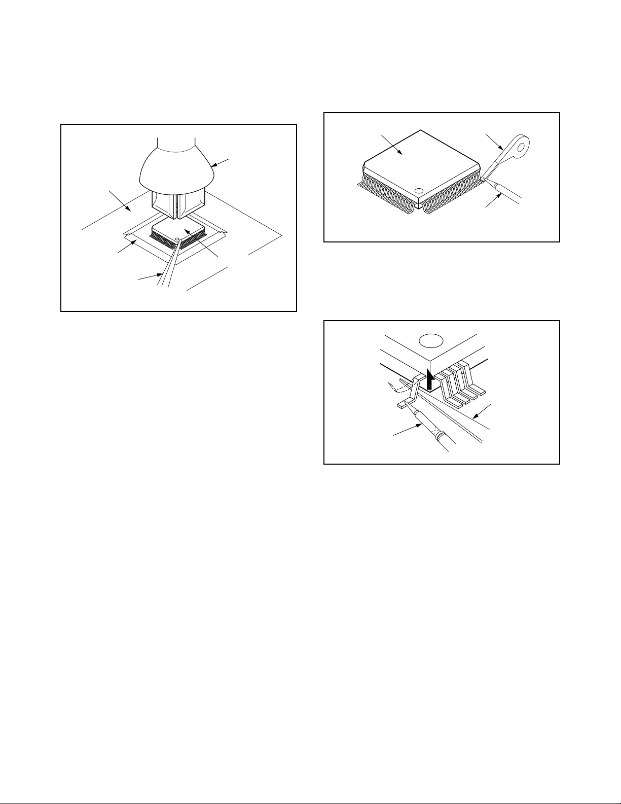
around the flat pack-IC to protect other parts from
damage. (Fig. S-1-2)
3. The flat pack-IC on the CBA is affixed with glue, so
be careful not to break or damage the foil of each
pin or the solder lands under the IC when
removing it.
Hot-air
Flat Pack-IC
Desoldering
CBA
Machine
With Soldering Iron:
1. Using desoldering braid, remove the solder from
all pins of the flat pack-IC. When you use solder
flux which is applied to all pins of the flat pack-IC,
you can remove it easily. (Fig. S-1-3)
Flat Pack-IC
Desoldering Braid
Soldering Iron
Fig. S-1-3
Masking
Tape
Tweezers
Flat Pack-IC
Fig. S-1-2
2. Lift each lead of the flat pack-IC upward one by
one, using a sharp pin or wire to which solder will
not adhere (iron wire). When heating the pins, use
a fine tip soldering iron or a hot air desoldering
machine. (Fig. S-1-4)
Sharp
Pin
Fine Tip
Soldering Iron
3. Bottom of the flat pack-IC is fixed with glue to the
CBA; when removing entire flat pack-IC, first apply
soldering iron to center of the flat pack-IC and heat
up. Then remove (glue will be melted). (Fig. S-1-6)
4. Release the flat pack-IC from the CBA using
tweezers. (Fig. S-1-6)
Fig. S-1-4
4-2 TVDVDN_SN
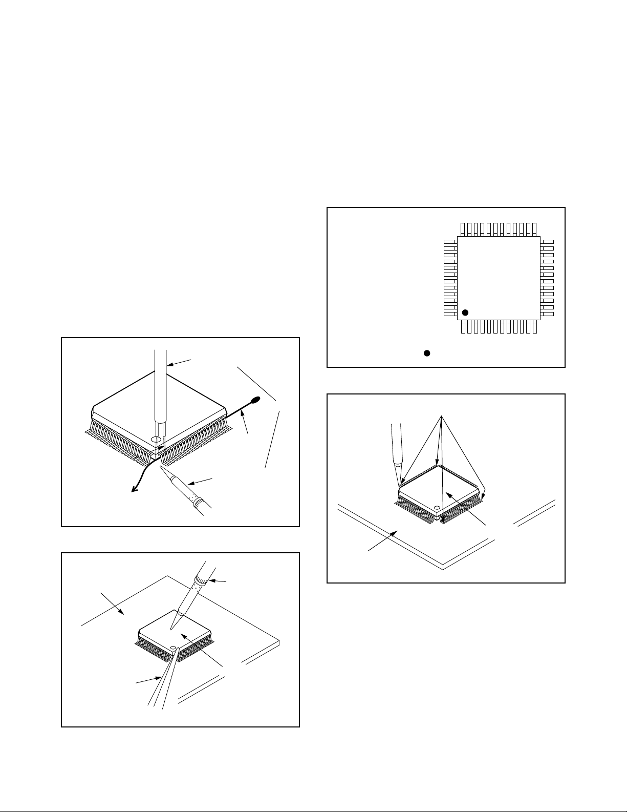
With Iron Wire:
1. Using desoldering braid, remove the solder from
all pins of the flat pack-IC. When you use solder
flux which is applied to all pins of the flat pack-IC,
you can remove it easily. (Fig. S-1-3)
2. Affix the wire to a workbench or solid mounting
point, as shown in Fig. S-1-5.
3. While heating the pins using a fine tip soldering
iron or hot air blower, pull up the wire as the solder
melts so as to lift the IC leads from the CBA
contact pads as shown in Fig. S-1-5.
4. Bottom of the flat pack-IC is fixed with glue to the
CBA; when removing entire flat pack-IC, first apply
soldering iron to center of the flat pack-IC and heat
up. Then remove (glue will be melted). (Fig. S-1-6)
5. Release the flat pack-IC from the CBA using
tweezers. (Fig. S-1-6)
Note: When using a soldering iron, care must be
taken to ensure that the flat pack-IC is not
being held by glue. When the flat pack-IC is
removed from the CBA, handle it gently
because it may be damaged if force is applied.
Hot Air Blower
2. Installation
1. Using desoldering braid, remove the solder from
the foil of each pin of the flat pack-IC on the CBA
so you can install a replacement flat pack-IC more
easily.
2. The “●” mark on the flat pack-IC indicates pin 1.
(See Fig. S-1-7.) Be sure this mark matches the 1
on the PCB when positioning for installation. Then
presolder the four corners of the flat pack-IC. (See
Fig. S-1-8.)
3. Solder all pins of the flat pack-IC. Be sure that
none of the pins have solder bridges.
Example :
Pin 1 of the Flat Pack-IC
is indicated by a " " mark.
Fig. S-1-7
To Solid
Mounting Point
CBA
Tweezers
Iron Wire
Soldering Iron
Fig. S-1-5
Fine Tip
Soldering Iron
Flat Pack-IC
or
Presolder
Flat Pack-IC
CBA
Fig. S-1-8
Fig. S-1-6
4-3 TVDVDN_SN
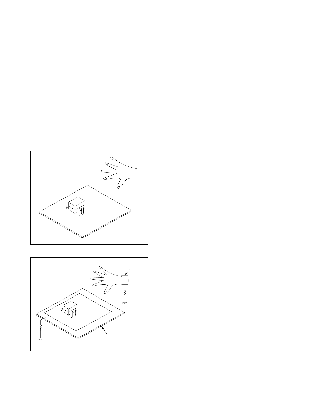
Instructions for Handling Semiconductors
Electrostatic breakdown of the semi-conductors may
occur due to a potential difference caused by
electrostatic charge during unpacking or repair work.
1. Ground for Human Body
Be sure to wear a grounding band (1 MΩ) that is
properly grounded to remove any static electricity that
may be charged on the body.
2. Ground for Workbench
Be sure to place a conductive sheet or copper plate
with proper grounding (1 MΩ) on the workbench or
other surface, where the semi-conductors are to be
placed. Because the static electricity charge on
clothing will not escape through the body grounding
band, be careful to avoid contacting semi-conductors
with your clothing.
<Incorrect>
<Correct>
1MΩ
CBA
Grounding Band
1MΩ
CBA
Conductive Sheet or
Copper Plate
4-4 TVDVDN_SN
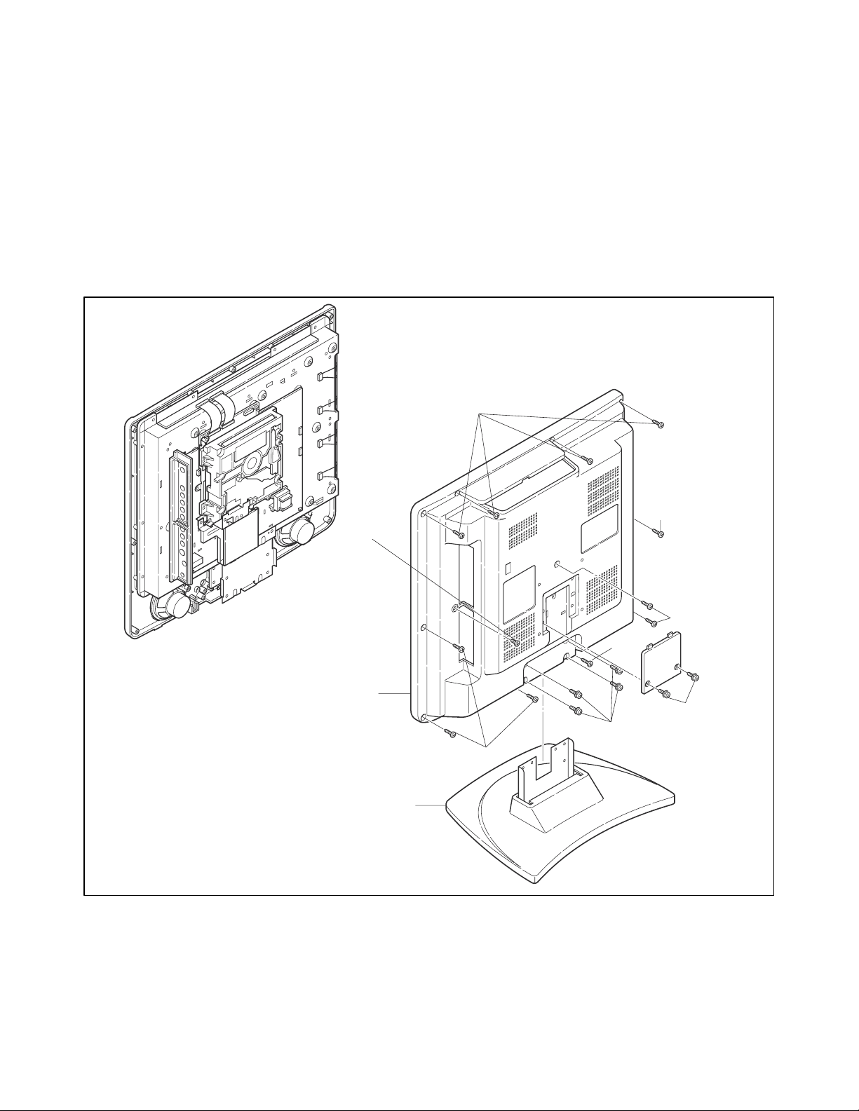
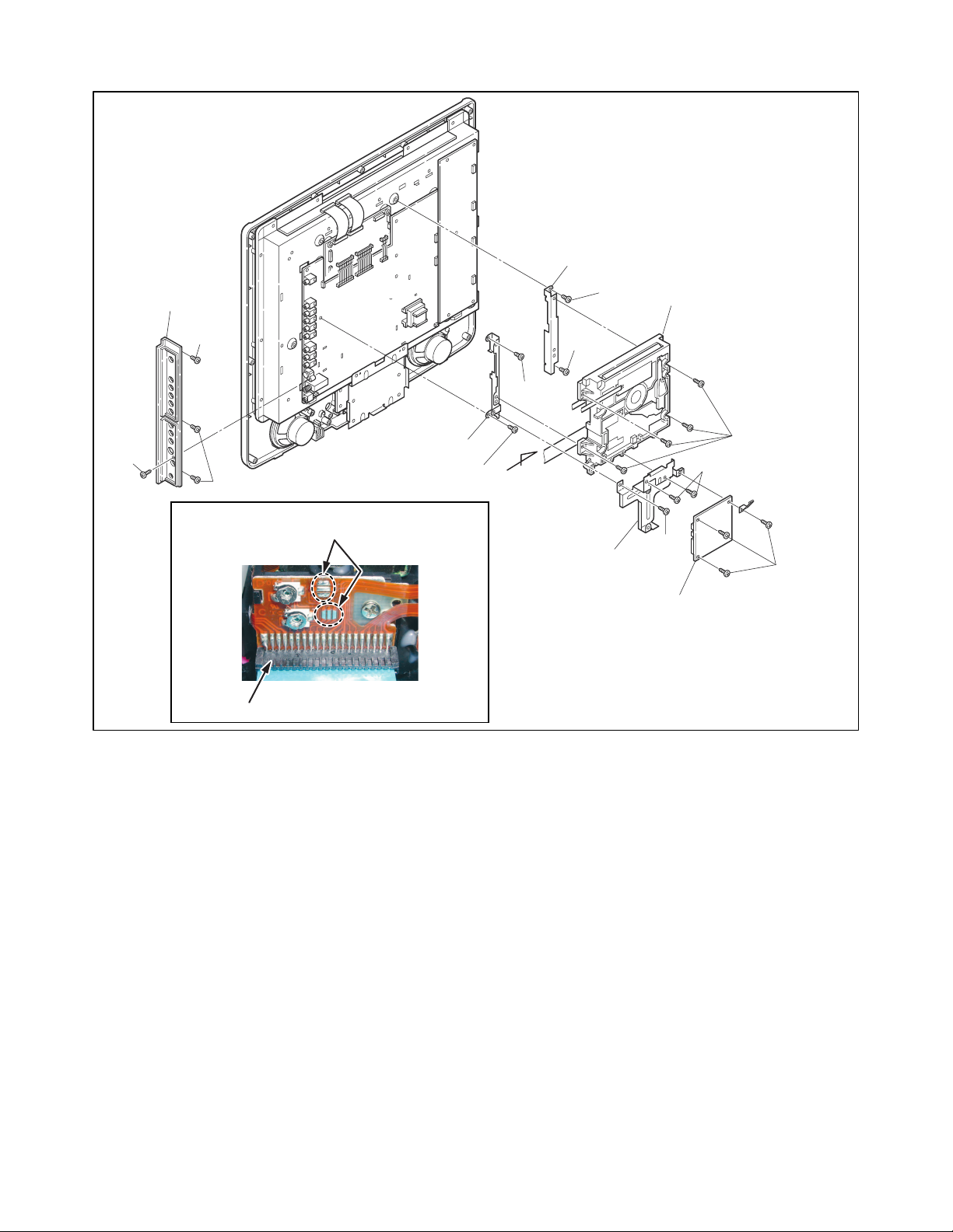
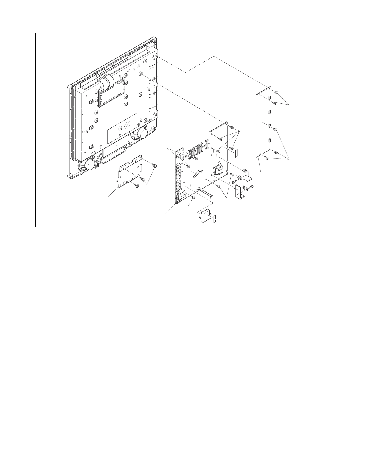
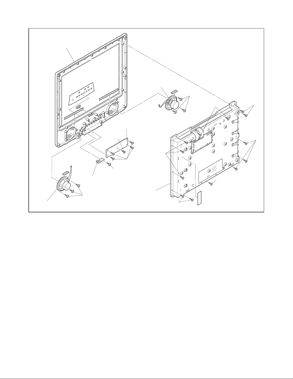
CABINET DISASSEMBLY INSTRUCTIONS
1. Disassembly Flowchart
This flowchart indicates the disassembly steps for the
cabinet parts, and the CBA in order to gain access to
item(s) to be serviced. When reassembling, follow the
steps in reverse order. Bend, route and dress the
cables as they were.
[14] Speaker(R)
[2] Jack Holder
[12] Function
CBA
[1] Rear Cabinet
[3] DVD Main
CBA Unit
[4] Loader
PCB Holder
[5] DVD
Mechanism
[6] DVD
Holder(R)
[8] Main CBA
[13] IR Sensor
CBA
[15] Speaker(L)
[9] Inverter
CBA
[7] DVD
Holder(L)
Step/
Loc.
Part
No.
[8] Main CBA
Inverter
[9]
CBA
Tilt Stand
[10]
Holder
LCD Main
CBA &
[11]
Liquid
Crystal
Panel Unit
Function
[12]
CBA
IR Sensor
[13]
CBA
Removal
Remove/*Unhook/
Fig.
No.
Unlock/Release/
Unplug/Unclamp/
Note
Desolder
9(S-11), *CN101A,
*CN102A, *CN103A,
D3
*CN801, *CN802,
D5
*CN1651, *CN411
D3D55(S-12), *CN450,
*CN460, *CN490
D3 2(S-13), (S-14) ---
D4D513(S-15), *CLN104,
*CLN105, *CN1751
D4
5(S-16) ---
D5
D4
(S-17) ---
D5
---
---
---
[11] LCD Main CBA &
Liquid Crystal Panel Unit
[16] Front Cabinet
[10] Tilt Stand
Holder
2. Disassembly Method
Removal
Step/
Loc.
Part
No.
Rear
[1]
Cabinet
[2] Jack Holder D2 3(S-4), (S-5) ---
DVD Main
[3]
CBA UnitD2D5
Loader
[4]
PCB Holder
DVD
[5]
Mechanism
DVD
[6]
Holder(R)
Remove/*Unhook/
Fig.
No.
Unlock/Release/
Unplug/Unclamp/
Desolder
11(S-1), (S-2), 4(S-3),
D1
Tilt Stand Assembly
3(S-6), *CN201,
*CN301, *CN401,
*CN601, *CN801
D2 (S-7A), 2(S-7B) ---
D2 4(S-8) 2
D2 2(S-9) ---
Note
---
1
[14] Speaker(R)
[15] Speaker(L)
Front
[16]
Cabinet
↓
(1)
↓
(2)
D4
3(S-18) ---
D5
D4
3(S-19) ---
D5
D4 --------------- ---
↓
(3)
↓
(4)
↓
(5)
Note:
(1) Order of steps in procedure. When reassembling,
follow the steps in reverse order. These numbers
are also used as the Identification (location) No. of
parts in figures.
(2) Parts to be removed or installed.
(3) Fig. No. showing procedure of part location
(4) Identification of parts to be removed, unhooked,
unlocked, released, unplugged, unclamped, or
desoldered.
P = Spring, L = Locking Tab, S = Screw,
CN = Connector
* = Unhook, Unlock, Release, Unplug, or Desolder
e.g. 2(S-2) = two Screws (S-2),
2(L-2) = two Locking Tabs (L-2)
(5) Refer to the following "Reference Notes in the
Table."
[7]
DVD
Holder(L)
D2 2(S-10) ---
5-1 L3250DC
Reference Notes
1. CAUTION 1: Electrostatic breakdown of the laser
diode in the optical system block may occur as a
potential difference caused by electrostatic charge
accumulated on cloth, human body etc., during
unpacking or repair work.
To avoid damage of pickup follow next procedures.
1) Short the three short lands of FPC cable with
solder before removing the FFC cable (CN201)
from it. If you disconnect the FFC cable
(CN201), the laser diode of pickup will be
destroyed. (Fig. D2)
2) Disconnect Connectors (CN301), (CN401),
(CN601) and (CN801). Remove three Screws
(S-6) and remove the DVD Main CBA Unit.
(Fig. D2)
2. CAUTION 2: When reassembling, confirm the
FFC cable (CN201) is connected completely. Then
remove the solder from the three short lands of
FPC cable. (Fig. D2)
3. How to eject a disc in emergency
Press and hold [EJECT] on the unit for more than
5 seconds.
(S-1)
(S-2)
[1] Rear Cabinet
Tilt Stand Assembly
(S-1)
(S-1)
(S-1)
(S-3)
(S-1)
Fig. D1
5-2 L3250DC
[6] DVD Holder(R)
[2] Jack Holder
(S-4)
(S-5)
Short the three short lands by soldering.
(Either of two places.)
Connector
(S-4)
[7] DVD Holder(L)
View for A
(S-10)
A
(S-10)
(S-9)
(S-9)
[4] Loader
PCB Holder
[5] DVD Mechanism
(S-8)
(S-7B)
(S-7A)
(S-6)
[3] DVD Main
CBA Unit
Fig. D2
5-3 L3250DC
(S-13)
(S-12)
(S-11)
(S-11)
(S-12)
[9] Inverter CBA
[10] Tilt Stand
Holder
(S-14)
[8] Main CBA
(S-11)
(S-11)
Fig. D3
5-4 L3250DC
[16] Front Cabinet
[14] Speaker(R)
(S-18)
[15] Speaker(L)
[12] Function CBA
(S-16)
(S-16)
(S-17)
[13] IR Sensor CBA
[11] LCD Main CBA &
(S-19)
Liquid Crystal Panel Unit
(S-15)
(S-15)
(S-15)
(S-15)
(S-15)
(S-15)
Fig. D4
5-5 L3250DC
TV Cable Wiring Diagram
To DVD Mechanism
LCD
Main CBA
To Liquid
Crystal
Panel
CN104
Function CBA
CLN104
IR Sensor CBA
CN201
CN601
CN301
CN801
CN401
DVD Main
CBA Unit
CN113
CN1701
CN801
CN103A
CN311
CN1751
CN1761
CN103B
CN101ACN102A
CN1651
CN312
CN102B
Main CBA
CN105
CN111
CN112
CN101B
CN411
CN802
CLN105
CN460
Inverter CBA
CLN411
CN490 CN450
To Speaker
To Liquid
To Speaker
Crystal
Panel
Fig. D5
5-6 L3250DC

3. How to Eject Manually
1. Remove the Rear Cabinet.
2. To remove the Loader PCB Holder with the DVD
Main CBA Unit, remove three screws (S-7) in Fig.
D2. Do not disconnect connectors.
3. To remove the Chassis Cover, remove 4 screws A
as shown in Fig. D6.
4. Remove a disc.
Chassis Cover
Disc
Screws A
Fig. D6
Reassembly note of the Chassis Cover:
1. Insert the pin A on the Chassis Cover into the hole
A on the Main Chassis as shown in Fig. D7.
Chassis Cover
Pin A
Hole A
Main Chassis
2. Tighten 4 screws A as shown in Fig. D6.
Fig. D7
5-7 L3250DC
ELECTRICAL ADJUSTMENT INSTRUCTIONS
General Note: “CBA” is abbreviation for
“Circuit Board Assembly.”
Note: Electrical adjustments are required after
replacing circuit components and certain
mechanical parts. It is important to perform
these adjustments only after all repairs and
replacements have been completed.
Also, do not attempt these adjustments unless
the proper equipment is available.
Test Equipment Required
1. DC Voltmeter
2. NTSC Pattern Generator (Color Bar W/White
Window, Red Color, Dot Pattern, Gray Scale,
Monoscope, Multi-Burst)
3. Remote control unit: Part No. NE240UD
4. Color Analyzer
How to make Service remote
control unit:
1. Prepare normal remote control unit (Part No.
NE240UD). Remove 3 screws from the back lid
(Fig. 1-1).
Screws
How to set up the service mode:
Service mode:
1. Use the service remote control unit.
2. Turn the power on. (Use main power on the TV
unit.)
3. Press [DISC MENU] button on the service remote
control unit. Version of micro computer will be
displayed on the LCD or display. (Ex: A95FP-0.23)
1. Initial Setting
General: Enter the Service mode. (See page 6-1.)
Set the each initial data as shown on table 1 below.
Table 1: Initial Data
Button
[Use the attached
Item
BRT
CNT 140
CLR-R 64
CLR-B 64
remote control unit.
(not service remote
control unit)]
[MENU] → [1]
Data
Value
120
Remote control unit (bottom)
2. Cut off pin 10 of the remote control
microprocessor and short circuit pins 10 and 17 of
the microprocessor with a jumper wire.
Fig. 1-1
TNT 128
V-TN T 12 8
SHR 35
S-BRT
S-CNT 140
S-CLR-R 64
[MENU] → [2]
S-CLR-B 64
S-TNT 128
S-SHR 35
C-BRT
C-CNT 144
C-CLR-R 69
[MENU] → [3]
C-CLR-B 69
C-TNT 128
C-SHR 35
120
124
6-1 L3250EA

Button
[Use the attached
Item
D2-BRT
D2-CNT 145
remote control unit.
(not service remote
control unit)]
Data
Value
135
3. If Flicker Adjustment is not fit, the screen becomes
the following.
VCOM
110
D2-CLR-R 68
D2-CLR-B 68
D2-TNT 128
D2-SHR 35
D3-BRT
D3-CNT 144
D3-CLR-R 69
D3-CLR-B 69
D3-TNT 128
D3-SHR 28
DR(C/D1)
C-DR(C/D2) 176
DB(C/D1)
C-DB(C/D2) 147
[MENU] → [5]
120
[MENU] → [6]
176
[VOL p] → [4]
147
[VOL p] → [6]
2. Flicker Adjustment
FLASH (Go and Off)
4. Press [CH. o / p] buttons on the remote control
unit so that flash stops.
1. Enter the Service mode. (See page 6-1.)
2. Press [2] button on the remote control unit.
The following screen appears.
VCOM
110
6-2 L3250EA

The following adjustment normally are not
attempted in the field. Only when replacing the
LCD Panel then adjust as a preparation.
3. White Balance Adjustment
Purpose: To mix red, green and blue beams correctly
for pure white.
Symptom of Misadjustment: White becomes bluish
or reddish.
Test Point Adj. Point Mode Input
[RF/VIDEO1]
Screen
VOL. p
buttons
M. EQ. Spec.
C/D1
[VIDEO2]
C/D2
White Purity
(APL 80%)
5. [RF/VIDEO1]
When “x” value and “y” value are not within
specification, adjust “DB (C/D1)” or “DR (C/D1)”.
Refer to “1. Initial Setting.”
Note: “DB(C/D1)” or “DR(C/D1)” must be adjusted
within ±0.01.
[VIDEO2]
When “x” value and “y” value are not within
specification, adjust “DB(C/D2)” or “DR(C/D2)”.
Refer to “1. Initial Setting.”
Note: “C-DB(C/D2)” or “C-DR(C/D2)” must be
adjusted within ±0.01.
6. Turn the power off and on again. (Main power
button on the TV unit.)
Pattern Generator,
Color analyzer
x: 0.256 to 0.316,
y: 0.264 to 0.324
Figure
It carries out in a darkroom.
Perpendicularity
L = 3 cm
INPUT: WHITE 80%
Note: Use the remote control unit.
1. Operate the unit for more than 20 minutes.
2. Input the White Purity (APL 80%).
3. Set the color analyzer to the CHROMA mode and
bring the optical receptor to the center on the
LCD-Panel surface after zero point calibration as
shown above.
Note: The optical receptor must be set
perpendicularly to the LCD Panel surface.
4. [RF/VIDEO1]
Enter the Service mode. Press “VOL p” button on
the remote control unit and select “C/D1-” mode.
[VIDEO2]
Enter the Service mode. Press “VOL p” button on
the remote control unit and select “C/D2-” mode.
Color Analyzer
6-3 L3250EA

HOW TO INITIALIZE THE LCD TV/DVD
To put the program back at the factory-default, initialize the LCD TV/DVD as the following procedure.
< DVD Section >
1. Press [1], [2], [3], [4], and [DISPLAY] buttons on the
remote control unit in that order.
Fig. g appears on the screen.
"
" differ depending on the models.
*******
MODEL : *******
Version
Region
Version
Region
: *.**
: *
EXIT: SELECTEEPROM CLEAR : CLEAR
Fig. g
"
" differ depending on the models.
*******
: *.**
: *
2. Press [CLEAR] button on the remote control unit.
Fig. h appears on the screen.
MODEL : *******
< LCD TV Section >
1. Turn the power on. (Use main power on the TV
unit.)
2. To enter the service mode, press [DISC MENU]
button on the service remote control unit.
- To cancel the service mode, press [POWER]
button on the remote control.
3. To initialize the LCD television, press [DISPLAY]
button on the remote control unit.
4. Confirm "FF" indication on the upper right of the
screen.
5. Unplug the AC cord.
EEPROM CLEAR : OK
EXIT: SELECTEEPROM CLEAR : CLEAR
Fig. h
When “OK” appears on the screen, the factory
default will be set.
3. To exit this mode, press [CH. o / p] or [SELECT]
button to go to TV mode, or press [POWER] button
to turn the power off.
7-1 L3150INT

FIRMWARE RENEWAL MODE
1. Turn the power on and press [EJECT] button on the
remote control unit to put the LCD TV/DVD into
DVD mode. Then remove the disc.
2. To put the LCD TV/DVD into F/W version up mode,
press [9], [8], [7], [6], and [SEARCH MODE] buttons on the remote control unit in that order.
Fig. a appears on the screen.
"
" differ depending on the models.
*******
F/W Version Up Mode Model No : *******
Please insert a DISC
for F/W Version Up.
VERSION : *.**
EXIT: SELECT
Fig. a Version Up Mode Screen
3. Insert the disc for version up into the disc slot.
4. The LCD TV/DVD enters the F/W version up mode
automatically. Fig. c appears on the screen. If you
enter the F/W for different models, “Disc Error” will
appear on the screen, then the disc will be ejected
automatically.
"
" differ depending on the models.
*******
5. After programming is finished, the disc will be
ejected automatically. Fig. e appears on the screen
and the checksum will be shown in (*2).
"
" differ depending on the models.
*******
(*2)
F/W Version Up Mode
VERSION : ************.ab6
Completed
SUM : 7ABC
Model No : *******
VERSION : *.**
Fig. e Completed Program Mode Screen
At this time, no button is available.
6. Remove the disc.
7. Press [CH. o / p] button on the unit to go to TV
mode, or press [POWER] button on the unit to turn
the power off.
8. Press [EJECT] button on the remote control unit to
put the LCD TV/DVD into DVD mode again.
9. Press [1], [2], [3], [4], and [DISPLAY] buttons on the
remote control unit in that order.
Fig. g appears on the screen.
"
" differ depending on the models.
*******
(*1)
F/W Version Up Mode Model No : *******
VERSION : ************.ab6
Reading...
VERSION : *.**
Fig. c Programming Mode Screen
The appearance shown in (*1) of Fig. c is
described as follows:
AppearanceNo. State
Reading... Sending files into the memory
1
Erasing... Erasing previous version data
2
Programming...
3 Writing new version data
MODEL : *******
Version
Region
: *.**
: *
EXIT: SELECTEEPROM CLEAR : CLEAR
Fig. g
10.Press [CLEAR] button on the remote control unit.
Fig. h appears on the screen.
"
" differ depending on the models.
*******
MODEL : *******
Version
Region
: *.**
: *
EXIT: SELECTEEPROM CLEAR : CLEAR
EEPROM CLEAR : OK
Fig. h
When “OK” appears on the screen, the factory
default will be set. Then the firmware renewal
mode is complete.
11.To exit this mode, press [CH. o / p] or [SELECT]
button to go to TV mode, or press [POWER] button
to turn the power off.
8-1 L3150FW

BLOCK DIAGRAMS < LCD TV SECTION >
System Control Block Diagram
KEY SWITCH
KEY SWITCH
SENSOR
REMOTE
RCV102
FUNCTION CBA
CLN114
KEY-IN-122
KEY-IN-211
CN104
CLN105
CN105
IR SENSOR CBA
RCV-IN33
TO
LCD BACKLIGHT
BLOCK DIAGRAM
P-ON-H
BACKLIGHT-SW
BACKLIGHT-ADJ
INVERTER CBA
CLN411
BACKLIGHT-ADJ
BACKLIGHT-SW
P-ON-H11 11
99
88
CN411
TO POWER SUPPLY
BLOCK DIAGRAM
P-ON-H
DVD-PWR-CON
CN113 IS USED
FOR ADJUSTMENT
AT FACTORY
TO IF/VIDEO
BLOCK DIAGRAM
FSC
SCL
SDA
S-SW
INPUT-0
AFT-IN
INPUT-1
P-ON-H
VOLUME
TO AUDIO
BLOCK DIAGRAM
SCL
DVD-MUTE
AUDIO-MUTE
SDA
SDA2
SCL1
BUS-OPEN
4
CN113 (NO CONNECTION)
IC333 (TV MICRO CONTROLLER)
4KEY-IN-2
3
KEY-IN-1
MAIN CBALCD MAIN CBA UNIT
CN102A
FSC123
BACKLIGHT-SW
BACKLIGHT-ADJ
P-ON-H16 8
INPUT-012 12
INPUT-111 13
P-ON-H2(NU)
DVD-PWR-CON
19 5
21 3
14 10
18 6
AL+3.3V(D)
5
RESET
IC151
4
21
11
RESET
RCV-IN
DVD-MAIN-POWER
P-25V-ON
26
12
X161
27MHz
42
43
XIN
XOUT
DVD-CS
DVD-SIN
DVD-SCLK
24
2737333639
25
REMOTE-OUT
DVD-IRCONT
DISC-OUT
CN102B
221817
80
TUNERCLK
BACKLIGHT-SW
DISC-IN
BACKLIGHT-ADJ
16
P-ON-H
P-ON-H2
3140193241
INPUT-0
INPUT-1
VOLUME15 9
S-SW717
SCL618
SDA519
AFT-IN10 14
5AFT-IN
20
SCL
SDA
S-SW
VOLUME
AUDIO-MUTE
DVD-MUTE
13 11
23 1
34
23
35
DVD-MUTE
BUS-OPEN
AUDIO-MUTE
Q301
Q131
BUFFER
AL+3.3V(D)
3.3V<-->5V
CONVERTER
BUS-OPEN519
CN103B CN103A
TO POWER
DVD-MAIN-POWER
SUPPLY
P-25V-ON
BLOCK
DIAGRAM
FP-DIN
FP-CLK
SDATA
REMOTE
TO
SYSTEM CONTROL
TREDCONTV
DISC-OUT
DISC-IN
/SERVO
BLOCK DIAGRAM
<DVD SECTION>
DVD-PWR-CON
9-1
IC171
(MEMORY)
7
WP
CN112(NO CONNECTION)
6
5
SCL
SDA
SDA 2
SCL 1
BUS-OPEN 4
NO PART
MOUNTED
FOR CN112
L3250BLS

IF/Video Block Diagram
TO
CVBS11
CN103A
LCD BLOCK
DIAGRAM
CN103B
S-VIDEO-C7
S-VIDEO-Y9
WF8
TO
VIDEO-Y5
CN103A
LCD BLOCK
DIAGRAM
CN103B
VIDEO-Pb/Cb
VIDEO-Pr/Cr
3
1
AUDIO SIGNAL
MAIN CBA
VIDEO SIGNAL
TO AUDIO BLOCK
DIAGRAM
SIF
8
SIF
AMP
7
4.5MHz
FILTER
CF31
4
SIF
TRAP
IF AGC DET
WF7
Q703
3
BUFFER
BUFFER
4
5
WF9
Q702
13
BUFFER
14
12
Q701
1
BUFFER
15
2
SW
TO AUDIO
BLOCK DIAGRAM
INPUT-0(INV)
INPUT-1(INV)
11
10
CONTROL
9
Q707
Q708
INPUT-0
INPUT-1
TO SYSTEM CONTROL
BLOCK DIAGRAM
TO SYSTEM CONTROL
BLOCK DIAGRAM
AFT-IN
13
18
IC781 (INPUT SELECT)
Q32
EQ
AMP
1
2
DEFEAT
VIDEO
VIF
IC31 (IF SIGNAL PROCESS)
16
SAW
FILTER
SF11
IF
TU1
(TUNER UNIT)
DET
AMP
17
VCO
RF
AGC
14
5
173
AGC
XTAL-IN
2
SCL
AFT
DVD-Y
TP1805
AMP
11
FSC
SCL
SDA
S-SW
SDA
JK703
<LCD TV SECTION>
VIDEO1
TO
SYSTEM CONTROL
BLOCK DIAGRAM
CY
-IN
JK701
S-VIDEO
IN
WF13
CN1701
CN601
TO DIGITAL
9-2
3
1
9 DVD-C
8 DVD-Y
VIDEO-C
VIDEO-Y(I/P)
SIGANL
PROCESS
BLOCK
DIAGRAM
TP1806
WF14
CHROMA
DVD MAIN CBA UNIT
Q704
WF10
BUFFER
Q705
JK706
VIDEO-YINJK707
WF11
BUFFER
Q706
VIDEO-Pb/CbINJK708
WF12
BUFFER
VIDEO-Pr/Cr
IN
L3250BLIF

Audio Block Diagram
TO
DIGITAL
SIGNAL
PROCESS
BLOCK
SPDIF
PCM-BCK
PCM-DATA
PCM-LRCLK
768
16
PORT
AUDIO
SERIAL
ZERO DETECT
CONTROLLER
DIGITAL FILTER /FUNCTION
DIAGRAM
TO
SYSTEM
CONTROL
DATA(AUDIO) SIGNAL
PCM-SCLK
AUDIO-MUTE
5
AUDIO SIGNAL
(AUDIO DAC)
IC601
/SERVO
BLOCK
DIAGRAM
<DVD
SECTION>
ADAC-ML
ADAC-MD
ADAC-MC
432
PORT
SERIAL
CONTROL
MANAGER
SYSTEM CLOCK
4X/8X OVERSAMPLING
15
L-CH
R-CH
LPF+AMP
DAC
ENHANCED
MULTI-LEVEL
DELTA-SIGMA
14
LPF+AMP
DAC
MODULATOR
DVD MAIN CBA UNIT
CN601CN1701
WF15
WF16
14
13
DVD-MUTE
DVD-AUDIO(L)
7
6
15
18
DVD-AUDIO(R)
SPDIF
8
11
BUFFER
WF17
JK1701
Q1701
TP1802
DIGITAL
AUDIO OUT
FR
CLN802
CN802
(COAXIAL)
SP802
SPEAKER
L-CH
GND 2
SP-L 1
11
AMP
VOLUME
JK801
HEADPHONE
JACK
14
AMP
WF6
SP801
SPEAKER
R-CH
CLN801
GND 2
SP-R 1
CN801
TO SYSTEM
CONTROL BLOCK
< LCD TV SECTION>
TO IF/VIDEO
BLOCK DIAGRAM
VOLUME
P-ON-H
AUDIO-MUTE
Q803
7
Q802
SCL
SDA
DVD-MUTE
INPUT-0(INV)
INPUT-1(INV)
IC851 (MTS/SAP AUDIO SIGNAL PROCESS)
SIF/BB
SW
INPUT
VCA
SIF
DEMOD
21
STEREO
FILTER
SAP
FILTER
OFFSET
CANCEL
SAP
DEMOD
WIDE BAND
FILTER
dBX
DE-EMPH
SPECTRAL
FILTER
L+R
FILTER
L-R
FILTER
SAP OUT
FILTER
WIDE BAND
RMS DET
SPECTRAL
EXPAND
SPECTRAL
RMS DET
75uS
DE-EMPH
(L-R)/SAP SW
OFFSET
CANCEL
WIDE BAND
EXPAND
L-CH
30
I2C
DECORDER
OFFSET
CANCEL
MATRIX
AGC
R-CH
29
FL
TP1801
2
MUTE
/STANDBY
CONTROL
3
(R-CH)
TUNER
AUDIO1
4
(R-CH)
1
3
SW CTL
AUDIO2
5
2
(L-CH)
IC801 (AUDIO AMP)
6
8
27
24
13
TUNER
AUDIO2
AUDIO1
IC852 (INPUT SELECT)
111514
(L-CH)
12
SWITCHING
Q804
REG+5V
9 10
SIF
TO
IF/VIDEO BLOCK
DIAGRAM
MAIN CBA
AUDIO1(L)
-IN
JK704
JK705
AUDIO1(R)
-IN
JK709
AUDIO2(L)
-IN
JK710
AUDIO2(R)
-IN
9-3
L3250BLA

LCD Block Diagram
LCD MODULE
OR(0)34
OR(2)32
OR(3)31
OR(1)33
OR(4)30
OR(5)29
OG(0)27
OG(1)26
OG(2)25
OG(3)24
OG(4)23
OG(5)22
OB(0)20
OB(1)19
OB(2)18
OB(3)17
OB(4)16
OB(5)15
ER(0)6
ER(1)5
ER(2)4
ER(3)3
ER(4)2
ER(5)1
EG(0)50
EG(1)49
EG(2)48
EG(3)47
EG(4)46
EG(5)45
EB(0)43
EB(1)42
EB(2)41
EB(3)40
EB(4)39
EB(5)38
OFFEV12
STV113
CLKV14
HMS1-E7
HMS1-013
STH142
POL43
CLKH10
LP44
VIDEO SIGNAL
LCD MAIN CBA UNIT
CN311
170
169
166
R(ODD)
R
165
164
163
162
161
157
156
G(ODD)
G
155
154
153
152
148
B(ODD)
B
147
146
145
LCD RGB
138
137
SIGNAL
PROCESS
136
135
130
129
R(EVEN)
Y
CN312
128
127
126
125
G(EVEN)
Pb/Cb
118
117
116
115
114
113
Pr/Cr B(EVEN)
108
107
101
105
STV1
OFFEV
R365
106
CLKV
CN311
WF1
WF2
R392
144
143
CLKH1
ODDINV
R202
R394
139
172
STH-1
EVENINV
173
POL
WF4
R201
WF3
WF5
174
LP
IC333 (LCD DRIVE / SIGNAL PROCESS)
A/D
R
CVBS
68
CN103B
CVBS 13
TO
IF/VIDEO
S-VIDEO-Y 15
S-VIDEO-C 17
BLOCK
DIAGRAM
CN103A
A/D
G
VIDEO
SIGNAL
C
49
PROCESS
A/D
B
Y
71
9-4
A/D
74
A/D
52
CN103B
VIDEO-Y 19
TO
IF/VIDEO
A/D
60
21
23
VIDEO-Pr/Cr
VIDEO-Pb/Cb
BLOCK
DIAGRAM
CN103A
L3250BLLCD

Power Supply Block Diagram
NOTE:
The voltage for parts in hot circuit is measured using
hot GND as a common terminal.
REG+5V(3)
AL+7V(D)
+5V REG.
IC672
+7V REG.
IC531
TO SYSTEM
VT+33V
TO LCD BACKLIGHT
BLOCK DIAGRAM
AL+21V
AL+12V
+21V
TP402
For continued protection against risk of fire,
replace only with same type 4 A, 125V fuse.
CAUTION ! :
ATTENTION : Utiliser un fusible de rechange de même type de 4A, 125V.
4A/125V
REG+5V(2)
+5V REG.
IC671
Q505
Q509
CONTOROL
BLOCK DIAGRAM
< LCD TV SECTION >
P-ON-H
DVD-PWR-CON
IC533
Q512
Q513
PANEL+3.3V
PANEL+10.8V
PANEL+25V
PANEL-6V
CN101B
PANEL+3.3V
PANEL+10.8V
PANEL+25V73
PANEL-6V82
46
55
CN101A
+5V REG.
Q531
Q510
Q501
Q503
Q502
AL+5V
AL+5V22 2
CN102A CN102B
TO SYSTEM
CONTROL
P-25V-ON
P-25V-ON21 3
Q511
BLOCK
DIAGRAM
AL+7V(D)21 3
CN103A CN103B
AL+3.3V(D)
< LCD TV SECTION >
+3.3V
REG.
DVD-MAIN-POWER
IC191
DVD-MAIN-POWER
18 6
Q1653
Q1655
AL+1.5V(D)
+1.5V
REG.
IC192
Q1652
AL+3.3V(A)
+3.3V
REG.
IC193
LCD MAIN
CBA UNIT
Q1651
EV+1.2V
CN401
EV+1.2V
22
CN1761
CN1751
EV+1.2V
14 14
CN1651
+1.2V REG.
IC1652
DVD-ON+3.3V
EV+3.3V(D)
EV+3.3V(A)
DVD-ON+5V
EV+1.2V
EV+3.3V(D)
EV+3.3V(A)
EV+3.3V(A)
DVD-ON+3.3V
33
EV+1.2V
13 13
Q1656
DVD-ON+5V
44
55
66
77
88
EV+3.3V(D)
EV+3.3V(A)
EV+3.3V(A)
DVD-ON+3.3V
DVD-ON+5V
99
88
12 12
11 11
10 10
Q1654
Q1657
EV+9V
SENSOR+3.3V
DVD MAIN CBA UNIT
EV+9V
EV+9V
SENSOR+3.3V
99
10 10
25 25
EV+9V
EV+9V
SENSOR+3.3V
77
66
11
Q633
CAUTION !
Fixed voltage (or Auto voltage selectable) power supply circuit is used in this unit.
If Main Fuse (F601) is blown , check to see that all components in the power supply
circuit are not defective before you connect the AC plug to the AC power supply.
Otherwise it may cause some components in the power supply circuit to fail.
9
T601
HOT COLD
HOT CIRCUIT. BE CAREFUL.
4A/125V
AC601
7
BRIDGE
RECTIFIER
D605 - D608
L601
LINE
FILTER
F601
4A/125V
AC CORD
12
16
11
14
6
5
10
13
3
SWITCHING
Q601
15
2
CONTROL
Q603
SWITCHING
1
4
IC601
ERROR
2
3
VOLTAGE DET
9-5
MAIN CBA
L3250BLP

LCD Backlight Block Diagram
BACK
1
CN450
LIGHT
2
OVER VOLTAGE
Q451,452
PROTECTOR
BACK
1
CN490
LIGHT
2
OVER VOLTAGE
PROTECTOR
Q491,492
Q454,455
BACK
LIGHT
LCD MODULEINVERTER CBA
1
2
CN460
7 6 98 1 2
13 14
OVER VOLTAGE
PROTECTOR
IC402
(OP AMP)
OVER VOLTAGE
PROTECTOR
Q461,462
T450
9
3
10
425
RL401
CLN411
Q421,
Q426
9
T490
3
CURRENT
CONTROL
10
425
SWITCH
Q403
7
8
1
6
8
1
IC401 (DC-AC INVERTER CONTROL)
7
6
262723
OUTPUT
LOGIC1
24
OUTPUT
LOGIC2
457
OSC
T460
Q433
LOGIC
9
3
425
CURRENT
CONTROL
SWITCH
Q411
OVER
VOLTAGE
10
+8V
REG.
28
VCC
PROTECT
7
8
1
6
14
PWM2
13
11
12
PWM1
10
9
STANDBY
16
SLOW
START
MODE SW
1
AL+21V22
AL+21V11
CN411
AL+21V
MAIN CBA
TO
POWER
SUPPLY
BLOCK
AL+21V33
P-ON-H
BACKLIGHT-ADJ
BACKLIGHT-SW
DIAGRAM
TO SYSTEM CONTROL
BLOCK DIAGRAM
< LCD TV SECTION >
9-6
Q412
L3250BLLB

BLOCK DIAGRAMS < DVD SECTION >
System Control / Servo Block Diagram
TO
SYSTEM
CONTROL
BLOCK
DIAGRAM
< LCD TV SECTION >
IC101
(MICRO CONTROLLER)
IC462
+3.3V
RESET73
RESET
1 3
VREF
FOCUS DRIVE
FD-OFST
148
146
25
27
26
-
+
-
+
24
TRACKING
DRIVE
TD-OFST
147
139
-
+
-
+
SDATA
FP-CLK
FP-DIN
DVD-PWR-CON
CN1761
20
19
18
DVD-PWR-CON
19 FP-CLK
18
CN401
TO AUDIO
BLOCK
DIAGRAM
ADAC-ML
ADAC-MD
ADAC-MC
57
56
ADAC-MD
ADAC-MC
SPDL
76
312
645
-
+
-
+
86ADAC-ML
SLD
75
23
-
+
PCM-SCLK
AUDIO-MUTE
88
163
PCM-SCLK
AUDIO-MUTE
IC202
(OP AMP)
59DVD-PWR-CON
60FP-CLK
82
FP-DIN
SP-ROT
SL-ADS
143
140
1
2
3
TRAY-IN
66
7
6
5
REMOTE
TREDCONTV
23 REMOTE2322 SDATA2220 FP-DIN
67
61
SDATA
REMOTE
DISC-IN
DISC-OUT
1
25
21
TREDCONTV
1 DISC-OUT
21 DISC-IN
25
DISC-OUT
78
DISC-IN
81
LCD MAIN CBA UNIT
Q801
RESET
IC461
2 1
+3.3V
(SERVO DRIVE)
IC301
FOCUS
ACTUATOR
15
FS(+)
FS(-)
DRIVE
16
TS(+)
TS(-)
TRACKING
ACTUATOR
14
DRIVE
13
DVD MAIN CBA UNIT
1 NOTE:
Either IC461 or IC462 is used for DVD MAIN CBA UNIT.
TO DIGITAL SIGNAL
PROCESS BLOCK
DIAGRAM
SPINDLE
MOTOR
DRIVE
12
11
DRIVE CBA
9-7
SLED
MOTOR
17
TRAY-IN
DRIVE
18
CN301
SPINDLE
MOTOR
M
3SP(+)
4SP(-)
5TRAY-IN
6GND
SLED
MOTOR
7SL(-)
M
8SL(+)
+3.3V
Q804
CN801CN5001
SENSOR CBA
Q802
3
2
1
LED-POWER
3 DISC-IN
2 DISC-OUT
1
L3250BLSD
DISC-OUT
DISC-IN

Digital Signal Process Block Diagram
TO
AUDIO
BLOCK
DIAGRAM
TO
/IF VIDEO
BLOCK
DIAGRAM
FLASH
ROM
DATA(AUDIO) SIGNAL
DATA(VIDEO/AUDIO) SIGNAL VIDEO SIGNAL
DAT A
RAM
DSP
INST.
ROM
DECODER
STREAM
I/F
DAT A
RAM
I/O
INST.
ROM
PROCESSOR
SPDIF
PCM-BCK
177
170
PCM-DATA
171
AUDIO
I/F
UMAC
PCM-LRCLK
169
SERIAL
GENERAL
I/O
CPU
I/F
READ
MEMORY
INTERRUPT
CONTROLLER
TIMER
VIDEO-Y(I/P)
149
Y(I/P)
D/A
NTSC/PAL
VIDEO
WATCH DOG
TIMER
REMOTE
VIDEO-C
158
C
D/A
ENCODER
I/F
CONTROL
32BIT CPU
BCU
DAT A
INST
DEBUG
RAM
RAM
IC103 (FLASH ROM)
1
23~51
~
9
~
162548
FADR (0-19)
~
293638
FDQ (0-15)
~
45
SDRAM ADDRESS(0-11)
IC101 (MICRO CONTROLLER)
~
217
238
SDRAM ADDRESS(0-11)
~~
222629
IC501,502 (SDRAM)
EXTERNAL
MEMORY
I/F
1
2
35
SDRAM
DECODER
I/F
ECC
SDRAM DATA(0-15)
~~
18
252
SDRAM DATA(0-15)
~
~
134253
256
114
115
DMA
116
DVD/CD
RF
SIGNAL
117
132
CN201
C16
FORMATTER
PROCESS
CIRCUIT
131
134
A17
D18
192~212
CPU
I/F
BCU
WATCH DOG
5
9
GND(LD)
GND(CD-PD)
TIMER
INTERRUPT
TIMER
CONTROLLER
CD/DVD
83
TO SYSTEM
CONTROL/SERVO
BLOCK DIAGRAM
< DVD SECTION >
6
IC201
(SW)
4
1 3
CD DVD
FS
TS
FS(+)
CN201
FS(+) 2
FS(-)
FS(-) 3
TS(+)
TS(+) 1
TS(-)
TS(-) 4
DVD MAIN CBA UNIT
PICK-UP
UNIT
32BIT
CPU
INST.
ROM
DAT A
RAM
126
124
125
AMP
Q251,Q252
Q253,Q254
AMP
CN201
CD-LD 10
DVD-LD 8
PD-MONI 7
123
6
GND(DVD-PD)
133
129
130
F12
B15
E14
CD/DVD 19
DETECTOR
9-8
L3250BLD
SCHEMATIC DIAGRAMS / CBA'S AND TEST POINTS
Standard Notes
Many electrical and mechanical parts in this chassis have special characteristics. These characteristics often
pass unnoticed and the protection afforded by them cannot necessarily be obtained by using replacement
components rated for higher voltage, wattage, etc. Replacement parts that have these special safety
characteristics are identified in this manual and its supplements; electrical components having such features are
identified by the mark “#” in the schematic diagram and the parts list. Before replacing any of these components,
read the parts list in this manual carefully. The use of substitute replacement parts that do not have the same
safety characteristics as specified in the parts list may create shock, fire, or other hazards.
Notes:
1. Do not use the part number shown on these drawings for ordering. The correct part number is shown in the
parts list, and may be slightly different or amended since these drawings were prepared.
2. All resistance values are indicated in ohms (K = 10
3. Resistor wattages are 1/4W or 1/6W unless otherwise specified.
4. All capacitance values are indicated in µF (P = 10
5. All voltages are DC voltages unless otherwise specified.
Note of Capacitors:
ML --- Mylar Cap. PP --- Metallized Film Cap. SC --- Semiconductor Cap. L --- Low Leakage type
Temperature Characteristics of Capacitors are noted with the following:
B --- ±10% CH --- 0±60 ppm/°C CSL --- +350~-1000 ppm/°C
3
, M = 106).
-6
µF).
Tolerance of Capacitors are noted with the following:
Z --- +80~-20%
Note of Resistors:
CEM --- Cement Res. MTL --- Metal Res. F --- Fuse Res.
Capacitors and transistors are represented by the following symbols.
CBA Symbols
(Top View) (Bottom View)
+
Electrolytic Capacitor
(Bottom View)
Transistor or Digital Transistor
E C B
(Top View)
NPN Transistor
E C B
(Top View)
(Top View)
PNP Transistor
E C B
(Top View)
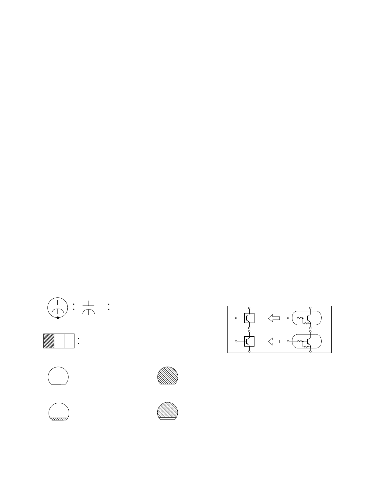
Schematic Diagram Symbols
Digital Transistor
E C B
NPN Digital Transistor
PNP Digital Transistor
E C B
10-1 L3150SC

LIST OF CAUTION, NOTES, AND SYMBOLS USED IN THE SCHEMATIC DIAGRAMS ON
THE FOLLOWING PAGES:
1. CAUTION:
CAUTION: FOR CONTINUED PROTECTION AGAINST RISK OF FIRE, REPLACE ONLY WITH SAME
TYPE_A,_V FUSE.
ATTENTION: UTILISER UN FUSIBLE DE RECHANGE DE MÊME TYPE DE_A,_V.
2. CAUTION:
Fixed Voltage (or Auto voltage selectable) power supply circuit is used in this unit.
If Main Fuse (F601) is blown, first check to see that all components in the power supply circuit are not
defective before you connect the AC plug to the AC power supply. Otherwise it may cause some components
in the power supply circuit to fail.
3. Note:
1. Do not use the part number shown on the drawings for ordering. The correct part number is shown in the
parts list, and may be slightly different or amended since the drawings were prepared.
2. To maintain original function and reliability of repaired units, use only original replacement parts which are
listed with their part numbers in the parts list section of the service manual.
4. Voltage indications for PLAY and STOP modes on the schematics are as shown
below:
< DVD Section >
Unit: Volts
The same voltage for
both PLAY & STOP modes
231
5.0
5.0
(2.5)
Indicates that the voltage
is not consistent here.
5. How to read converged lines
1-D3
Distinction Area
Line Number
(1 to 3 digits)
Examples:
1. "1-D3" means that line number "1" goes to the line number
"1" of the area "D3".
2. "1-B1" means that line number "1" goes to the line number
"1" of the area "B1".
6. Test Point Information
: Indicates a test point with a jumper wire across a hole in the PCB.
: Used to indicate a test point with a component lead on foil side.
PLAY mode
STOP mode
< TV Section > Unit: Volts
Unit: Volts
The same voltage for
both TV & DVD modes
231
5.0
5.0
(2.5)
< 0 >
Indicates that the voltage
is not consistent here.
TV mode (Power on)
TV mode (Power off)
DVD mode
3
AREA D3
2
1
AREA B1
1-D3
ABCD
1-B1
: Used to indicate a test point with no test pin.
: Used to indicate a test point with a test pin.
10-2 L3150SC

Main 1/4 Schematic Diagram
MAIN 1/4
Ref No. Position
IC531
D-4
IC533
E-3
IC671
E-2
IC672
E-2
Q501 C-4
Q502 C-4
Q503 B-3
Q505 C-3
Q509 C-3
Q510 B-2
Q511 C-3
Q512 C-2
Q513 C-2
Q531 D-3
Q633 E-1
CN101A A-4
CN102A A-3
CN411 F-4
CONNECTORS
ICS
TRANSISTORS
10-3
L3250SCM1

Main 2/4 Schematic Diagram
MAIN 2/4
Ref No. Position
IC31 I-1
IC851 H-3
IC852 J-4
Q32 J-2
CN113 G-1
CONNECTOR
ICS
TRANSISTOR
10-4
L3250SCM2

Main 3/4 Schematic Diagram
MAIN 3/4
Ref No. Position
IC781
P-3
IC801
N-2
Q701
N-3
Q702
N-3
Q703 N-3
Q704 P-1
Q705 O-1
Q706 P-1
Q707 P-2
Q708
P-2
Q802
O-1
Q803
N-1
Q804 O-2
Q1701 P-4
CN103A
M-2
CN801 M-3
CN802
M-4
CN1701 R-4
TP1801 Q-4
TP1802 Q-4
TP1803 Q-4
TP1804 Q-4
TP1805 Q-4
TP1806 Q-4
CONNECTORS
ICS
TRANSISTORS
TEST POINTS
10-5
L3250SCM3
Main 4/4 Schematic Diagram
NOTE:
The voltage for parts in hot circuit is measured using
hot GND as a common terminal.
MAIN 4/4
Ref No. Position
IC601
U-1
IC1652 W-3
Q601
S-2
Q603
T-2
Q1651 W-1
Q1652 W-1
Q1653 W-1
Q1654 W-3
Q1655 W-3
Q1656 W-2
Q1657 X-2
TP402 X-4
TRANSISTORS
ICS
TEST POINT
CAUTION !
Fixed voltage (or Auto voltage selectable) power supply circuit is used in this unit.
If Main Fuse (F601) is blown , check to see that all components in the power supply
circuit are not defective before you connect the AC plug to the AC power supply.
Otherwise it may cause some components in the power supply circuit to fail.
4A/125V
CAUTION ! :
ATTENTION : Utiliser un fusible de rechange de même type de 4A, 125V.
For continued protection against risk of fire,
replace only with same type 4 A, 125V fuse.
10-6
L3250SCM4

Inverter Schematic Diagram
INVERTER
Ref No. Position
IC401
A-3
IC402
E-3
Q403 B-1
Q411 B-3
Q412 B-3
Q421 B-4
Q426 B-3
Q433 B-2
Q451 E-4
Q452 D-4
Q454 D-3
Q455 D-3
Q461 E-2
Q462 D-2
Q491 D-3
Q492 D-3
CLN411
A-1
CN450 F-4
CN460
F-2
CN490 F-4
ICS
TRANSISTORS
CONNECTORS
10-7
L3250SCI

Function Schematic Diagram
10-8
L3250SCF

IR Sensor Schematic Diagram
10-9
L3250SCIR

LCD Main 1/2 Schematic Diagram
LCD MAIN 1/2
Ref No. Position
IC333
B-3
Q301
D-1
CN102B A-4
CN104
A-3
CN105
A-2
CN111
A-2
CN211
F-4
CN311 F-4
CONNECTORS
IC
TRANSISTOR
10-10
L3250SCL1

LCD Main 2/2 Schematic Diagram
LCD MAIN 2/2
Ref No. Position
IC151
I-3
IC171 J-3
IC191
H-2
IC192 H-1
IC193
H-2
IC201 J-1
Q131
I-4
Q201 J -1
CN101B
L-4
CN103B
G-2
CN112
L-4
CN312
L-3
CN1751 H-4
CN1761 G-4
ICS
CONNECTORS
TRANSISTORS
10-11
L3250SCL2

DVD Main 1/3 Schematic Diagram
DVD MAI N 1/3
Ref No. Position
IC201 C-1
IC202 D-4
IC301 D-3
IC461 F-1
IC462 E-1
Q251 C-2
Q252 B-2
Q253 C-2
Q254 B-2
Q801 B-1
Q802 B-1
Q804 B-1
CN201 A-3
CN301 A-2
CN401 F-3
CN801 A-1
ICS
TRANSISTORS
CONNECTORS
1 NOTE:
Either IC461 or IC462 is used for DVD MAIN CBA UNIT.
10-12
L3250SCD1

DVD Main 2/3 Schematic Diagram
10-13
L3250SCD2

IC101 Voltage Chart
PIN.NO PLAY STOP PIN.NO PLAY STOP PIN.NO PLAY STOP PIN.NO PLAY STOP
129 2.3 2.3 161 3.4 3.4 193 ~ ~ 225 3.4 3.4
130 2.3 2.3 162 0 0 194 ~ ~ 226 ~ ~
131 2.3 2.3 163 1.8 1.8 195 ~ ~ 227 ~ ~
132 2.4 2.3 164 0 0 196 3.4 3.4 228 ~ ~
133 2.4 2.4 165 1.7 1.8 197 ~ ~ 229 0 0
134 2.4 2.4 166 1.7 1.7 198 ~ ~ 230 ~ ~
135 2.3 2.3 167 3.4 3.4 199 ~ ~ 231 3.4 3.4
136 2.3 2.3 168 0 0 200 ~ ~ 232 1.3 1.6
137 2.3 2.3 169 1.8 1.8 201 0 0 233 ~ ~
138 2.3 2.3 170 1.7 1.7 202 3.4 3.4 234 1.9 2.3
139 1.7 1.7 171 1.3 0.1 203 ~ ~ 235 0 0
140 1.7 1.7 172 1.3 1.3 204 ~ ~ 236 1.3 1.3
141 3.4 3.4 173 0 0 205 0 0 237 ~ ~
142 1.3 1.3 174 ----- ----- 206 ~ ~ 238 ~ ~
143 2.1 1.7 175 ----- ----- 207 ~ ~ 239 3.4 3.4
144 2.2 2.2 176 ----- ----- 208 ~ ~ 240 3.4 3.3
145 0 0 177 1.8 1.7 209 3.4 3.4 241 1.9 1.9
146 1.7 1.7 178 3.4 3.5 210 ~ ~ 242 0 0
147 1.8 1.7 179 0 0 211 ~ ~ 243 1.9 1.9
148 1.7 1.7 180 ----- ----- 212 ~ ~ 244 3.4 3.3
149 0.6 0.5 181 ----- ----- 213 0 0 245 3.4 3.4
150 3.4 3.4 182 ----- ----- 214 2.5 3.0 246 3. 4 3.4
151 ----- ----- 183 ----- ----- 215 2. 5 3.0 247 0 0
152 ----- ----- 184 ----- ----- 216 3.4 3.4 248 3.3 3.4
153 1.4 1.3 185 ----- ----- 217 ~ ~ 249 3.2 3.0
154 1.4 1.3 186 ----- ----- 218 0 0 250 0 0
155 2.4 2.4 187 ----- ----- 219 1.3 1.3 251 3. 2 3.0
156 ----- ----- 188 ----- ----- 220 ~ ~ 252 ~ ~
157 0 0 189 ----- ----- 221 ~ ~ 253 0 0
158 0.9 0.9 190 3.4 3.5 222 0 0 254 ~ ~
159 3.4 3.4 191 0 0 223 ~ ~ 255 3.4 3.4
160 0 0 192 ~ ~ 224 ~ ~ 256 ~ ~
~ : Voltage is not cons istent ----- : Not used Unit : Volts
PIN.NO PLAY STOP PIN.NO PLAY STOP PIN.NO PLAY STOP PIN.NO PLAY STOP
1 ~ ~ 33 ~ ~ 65 ----- ----- 97 ----- -----
2 ~ ~ 343.43.4663.43.5983.43.4
3 0 0 35 0 0 673.23.2990.90.8
4 ~ ~ 36 ~ ~ 68 ----- ----- 100 0 0
5 ~ ~ 37 ~ ~ 69 3.4 3.4 101 2.4 2.4
6 3.4 3.4 38 0.4 0.3 70 3.4 3.4 102 2.2 2.2
7 ~ ~ 39 ~ ~ 71 ----- ----- 103 1. 9 1.9
8 ~ ~ 40 ~ ~ 72 1.4 2.7 104 0.4 0.3
9 0 0 41 ~ ~ 73 3.5 3.5 105 0 0
10 ~ ~ 42 ~ ~ 74 0 0 106 1.7 1.7
11 ~ ~ 43 ~ ~ 75 1.7 1.8 107 3.4 3.4
12 3.4 3.4 44 1.3 1.3 76 2.3 1.8 108 ----- -----
13 ~ ~ 45 ~ ~ 77 ----- ----- 109 ----- -----
14 ~ ~ 46 ~ ~ 78 0 0 110 1.9 1.9
15 ~ ~ 47 ~ ~ 79 ----- ----- 111 1.9 1.9
16 0 0 48 3.4 3.4 80 3.4 0 112 1.7 1.7
17 ~ ~ 49 0 0 81 0 0 113 1.7 1.7
18 ~ ~ 50 ~ ~ 82 ----- ----- 114 1.7 1.7
19 3.4 3.4 51 ~ ~ 83 0.1 0.1 115 1.7 1.7
20 0 0 52 0.8 0.8 84 3.4 3.4 116 1.7 1.7
21 ----- ----- 53 ----- ----- 85 ----- ----- 117 1.7 1.7
22 3.4 3.4 54 ----- ----- 86 3.6 3.4 118 3.4 3.4
23 ~ ~ 55 ----- ----- 87 0 0 119 2.0 2.0
24 ~ ~ 56 3.4 3.4 88 3.5 0.1 120 1.7 1.7
25 ~ ~ 57 3.5 3.5 89 1.3 1.3 121 1.5 1.5
26 1.3 1.3 58 3.4 3.4 90 ----- ----- 122 0 0
27 ~ ~ 59 3.4 3.4 91 ----- ----- 123 0.3 0.1
28 3.4 3.4 60 3.4 3.4 92 ----- ----- 124 1.1 0.1
29 0 0 61 3.5 3.5 93 0 0 125 0.3 0.1
30 ~ ~
31 ~ ~
32 ~ ~
62 3.4 3.4
63 0 0
64 0 0
94 ----- ----- 126 0.1 0.1
95 ----- ----- 127 2.3 2.3
96 ----- ----- 128 1.7 1.7
10-14

DVD Main 3/3 Schematic Diagram
DVD MAI N 3/3
Ref No. Position
IC103 N-3
IC501 N-4
IC502 P-4
IC601 P-1
CN601 R-1
ICS
CONNECTOR
10-15
L3250SCD3

Main CBA Top View
Because a hot chassis ground is present in the power
supply circuit, an isolation transformer must be used.
Also, in order to have the ability to increase the input
slowly,when troubleshooting this type power supply
circuit, a variable isolation transformer is required.
CAUTION !
Fixed voltage (or Auto voltage selectable) power supply circuit is used in this unit.
If Main Fuse (F601) is blown , check to see that all components in the power supply
circuit are not defective before you connect the AC plug to the AC power supply.
Otherwise it may cause some components in the power supply circuit to fail.
TP1802
FR
TP1803
A-GND
4A/125V
CAUTION ! :
ATTENTION : Utiliser un fusible de rechange de même type de 4A, 125V.
NOTE:
The voltage for parts in hot circuit is measured using
hot GND as a common terminal.
For continued protection against risk of fire,
replace only with same type 4 A, 125V fuse.
TP1801
FL
TP1805
DVD-Y
TP1806
CHROMA
TP1804
GND
TP402
+21V
10-16
BL3150F01011-1

Main CBA Bottom View
Because a hot chassis ground is present in the power
supply circuit, an isolation transformer must be used.
Also, in order to have the ability to increase the input
slowly,when troubleshooting this type power supply
circuit, a variable isolation transformer is required.
MAIN CBA
Ref No. Position Ref No. Position
IC31
E-4 Q601 B-5
IC531
D-4
Q603
B-5
IC533
D-3
Q633
A-5
IC601 A-5
Q701
D-2
IC671
D-4
Q702
D-2
IC672
D-4 Q703 D-2
IC781
E-2 Q704 E-1
IC801
D-5 Q705 E-1
IC851
D-2 Q706 E-2
IC852 E-3
Q707
E-2
IC1652 C-4
Q708
E-2
Q802
D-5
Q32 E-4
Q803
D-4
Q401 B-2 Q804 E -2
Q403 B-1 Q1651 C-4
Q404 B-1 Q1652 C-3
Q405 B-1 Q1653 C-3
Q406 B-1 Q1654 C-4
Q407 A-1 Q1655 C-4
Q408 C-1 Q1656 C-4
Q409 A-2 Q1657 C-4
Q410 B-1 Q1701 E-1
Q411 B-2
Q412 B-2 CN101A C-2
Q415 B-3 CN102A C-2
Q416 B-3 CN103A D-2
Q421 B-1
CN113
E-2
Q422 B-1
CN402
A-2
Q423 B-1
CN403
A-5
Q424 A-2
CN411
B-2
Q427 B-2
CN801
E-5
Q428 B-2
CN802
A-5
Q501 C-2 CN1701 E-2
Q502 C-2
Q503 C-2
TP402
A-3
Q505
C-3
TP403
B-1
Q509
C-3 TP1801 E-2
Q510
C-2 TP1802 E-2
Q511
C-2 TP1803 E-2
Q512 C-2 TP1804 E-2
Q513 C-3 TP1805 E-2
Q531 C-2 TP1806 E-3
TRANSISTORS
TEST POINTS
TRANSISTORS
CONNECTORS
ICS
CAUTION !
Fixed voltage (or Auto voltage selectable) power supply circuit is used in this unit.
If Main Fuse (F601) is blown , check to see that all components in the power supply
circuit are not defective before you connect the AC plug to the AC power supply.
Otherwise it may cause some components in the power supply circuit to fail.
4A/125V
CAUTION ! :
ATTENTION : Utiliser un fusible de rechange de même type de 4A, 125V.
NOTE:
The voltage for parts in hot circuit is measured using
hot GND as a common terminal.
WF7
PIN 11 OF
CN103A
For continued protection against risk of fire,
replace only with same type 4 A, 125V fuse.
WF8
PIN 9 OF
CN103A
WF9
PIN 7 OF
CN103A
WF12
Q706
Emitter
10-17
WF10
Q704
Emitter
WF11
Q705
Emitter
WF13
PIN 1 OF
CN1701
WF14
PIN 3 OF
CN1701
WF15
PIN 6 OF
CN1701
WF16
PIN 8 OF
CN1701
WF17
PIN 11 OF
CN1701
WF6
PIN 14
OF IC801
BL3150F01011-1

Inveretr CBA Top View
INVERTER
Ref No. Position
IC401
D-1
IC402
E-1
Q403 C-1
Q411 D-1
Q412 D-2
Q421 D-1
Q426 D-1
Q433 A-1
Q451 E-1
Q452 E-1
Q454 E-1
Q455 E-1
Q461 A-1
Q462 A-1
Q491 E-2
Q492 E-2
CLN411
C-1
CN450
C-2
CN460
A-2
CN490 D-2
ICS
TRANSISTORS
CONNECTORS
Inverter CBA Bottom View
10-18
BL3100F01022-1

Function CBA Top View
IR Sensor CBA Top & Bottom View
Function CBA Bottom View
BL3100F01022-2
BL3150F01011-3
10-19
BL3100F01022-2

WAVEFORMS < LCD TV SECTION >
WF1 ~ WF12 = Waveforms to be observed at
Waveform check points.
(Shown in Schematic Diagram.)
Input: NTSC Color Bar Signal (with 1kHz Audio Signal)
CLKH
WF1 1DIV: 1.0V 10
1DIV: 1.0V 10 s
R392
CLKV
WF2
1DIV: 1.0V 20ns
R365
STH1
WF5
AUDIO
WF6
R394
1DIV: 100mV 400
Pin 14 of IC801
S-VIDEO-C
s
WF9
1DIV: 200mV 20 s
Pin 7 of CN103A
VIDEO-Y
s
WF10
1DIV: 200mV 20
s
Q704 Emitter
POL
WF3 1DIV: 200mV 20
1DIV: 1.0V 20
s
R202
LP
WF4
1DIV: 1.0V 10
s
R201
CVBS
WF7
S-VIDEO-Y
WF8
Pin 11 of CN103A
1DIV: 200mV 20
Pin 9 of CN103A
11-1
VIDEO-Pb/Cb
s
WF11
1DIV: 200mV 20
s
Q705 Emitter
VIDEO-Pr/Cr
s
WF12
1DIV: 200mV 20
s
Q706 Emitter
L3250WF1

WAVEFORMS < DVD SECTION >
20
0.1V
DVD-Y
DVD-C
0.1V
20
DVD-AUDIO(L)1V1V
0.5ms
DVD-AUDIO(R)1V1V
0.5ms
SPDIF
1V
0.1
DVD-Y
WF13
DVD-C
WF14
Pin 1 of CN1701
0.1V
Pin 3 of CN1701
DVD-AUDIO(R)
WF16
SPDIF
WF17
Pin 8 of CN1701
1V
Pin 11 of CN1701
20
µ
s0.1V
20
µ
s
0.5ms
0.1
µ
s
DVD-AUDIO(L)
WF15
Pin 6 of CN1701
0.5ms
11-2
NOTE:
Input
CD: 1kHz PLAY
(WF15~WF17)
DVD: POWER ON (STOP) MODE
(WF13~WF14)
L3250WF2

WIRING DIAGRAM < LCD TV SECTION >
>
TO WIRING
DIAGRAM
<DVD SECTION
TO DVD
MAIN CBA
153
CN1761
DISC-OUT
CN1751
EV+1.2V
141012
EV+1.2V
CN1651
2
EV+1.2V
EV+1.2V
EV+3.3V(D)
EV+1.2V
13
EV+1.2V
EV+3.3V(D)
4
6
EV+3.3V(A)
EV+3.3V(A)
EV+3.3V(D)
DVD-ON+3.3V
EV+3.3V(A)
EV+3.3V(A)
9
1014121113
9
11
EV+3.3V(A)
EV+3.3V(A)
DVD-ON+3.3V
9
7
8
EV+9V
DVD-ON+5V
DVD-ON+3.3V
DVD-ON+5V
EV+9V
EV+9V
724
6
8
6
8
7
EV+9V
EV+9V
DVD-ON+5V
101412
11
GND
GND
EV+9V
GND
GND
GND
51342
GND
GND
GND
UNIT CN401
13
15
GND
GND
GND
SENSOR+3.3V
GND
153
GND
SENSOR+3.3V
16
GND
CN102B
CN102A
FP-DIN
DISC-IN
GND
BACKLIGHT-SW
51342
GND
BACKLIGHT-SW
24
SDATA
REMOTE
SENSOR+3.3V
DVD-PWR-CONNUP-ON-H
6
8
7
NU
P-ON-H
DVD-PWR-CON
18
17
1923212022
GND
FP-CLK
DVD-PWR-CON
BACKLIGHT-ADJ
DVD-MUTE
GND
232122192017181615
GND
DVD-MUTE
BACKLIGHT-ADJ
25
TREDCONTV
AUDIO-MUTE
VOLUME
P-ON-H2(NU)
INPUT-0
1411121310
9
11
INPUT-0
VOLUME
P-ON-H2(NU)
AUDIO-MUTE
PROTECT-1
INPUT-1
AFT-IN
PROTECT-2
S-SW
SCL
978563421
15
172220
18
16
141012
13
SCL
S-SW
AFT-IN
INPUT-1
PROTECT-1
PROTECT-2
SDA
GND
P-25V-ON
GND
AL+5V
231921
SDA
GND
GND
AL+5V
P-25V-ON
153
DVD-Y
CN1701
TU1 TUNER UNIT
AUDIO1
TO DVD
2
4
GND
GND
GND
DVD-C
SCL
(NO CONNECTION)
134
CN113
AUDIO1
(L)-IN
(R)-IN
MAIN CBA
UNIT CN601
7
6
DVD-MUTE
DVD-AUDIO(L)
GND
SDA
2
AUDIO2
9
8
10
11
SPDIF
DVD-AUDIO(R)
DVD-AUDIO+5V
DVD-AUDIO+5V
CN113 IS USED
FOR ADJUSTMENT
AT FACTORY
BUS-OPEN
AUDIO2
(L)-IN
(R)-IN
DIGITAL AUDIO OUT
(COAXIAL)
CN450
1
BACK
MAIN CBA
2
LIGHT
S-VIDEO
OUT IN
CLN411
AL+21V
153
153
CN411
AL+21V
CN490
VIDEO
-Pr/Cr IN
AL+21V
AL+21V
2
2
AL+21V
AL+21V
1
BACK
GND
4
4
GND
2
LIGHT
VIDEO
-Pb/Cb IN
GND
GND
6
6
GND
GND
GND
7
7
GND
VIDEO
BACKLIGHT-SW
8
8
BACKLIGHT-SW
CN460
1
BACK
-Y IN
BACKLIGHT-ADJ
9
9
BACKLIGHT-ADJ
2
LIGHT
PROTECT-1
10
10
PROTECT-1
VIDEO1
-IN
P-ON-H
11
11
P-ON-H
INVERTER CBA
NU
CN101A
1
NU
CN101B
GND
NU
386
2
895
7
NU
GND
PANEL+10.8V
GND
PANEL+3.3V
4
6
4
GND
PANEL+3.3V
PANEL+10.8V
PANEL+25V
PANEL-6V
3
2
PANEL-6V
PANEL+25V
GND
957
1
GND
CN103A
VIDEO-Pr/Cr
231921
CN103B
VIDEO-Pr/Cr
VIDEO-Pb/Cb
GND
GND
22
20
GND
GND
VIDEO-Pb/Cb
GND
VIDEO-Y
6
51342
18
GND
VIDEO-Y
S-VIDEO-C
GND
S-VIDEO-Y
8
9
7
15
17
16
GND
S-VIDEO-Y
S-VIDEO-C
GND
CVBS
GNDNUGNDNUAL+3.3V(A)
13
11
141012
13
11
NU
GND
GNDNUGND
CVBS
15
141012
9
AL+3.3V(A)
PROTECT-3
172220
16
8
7
PROTECT-3
BUS-OPEN
DVD-MAIN-POWER
18
6
51342
BUS-OPEN
DVD-MAIN-POWER
GND
GND
GND
AL+7V(D)
FSC
231921
FSC
GND
AL+7V(D)
LCD MAIN CBA
AL+5V
RCV-IN
GND
KEY-IN-2
CN104
132
1
CLN114
KEY-IN-2
AL+3.3V(D)
KEY-IN-1
3
2
KEY-IN-1
AL+3.3V(D)
GND
4
4
GND
5 NU
5
NU
FUNCTION CBA
CN105
132
1
AL+5V
CLN105
2
GND
NU
4
5 NU
CN801
SP-R
GND
1
3
4
NU5NU
RCV-IN
IR SENSOR CBA
2
CLN801
SP801
SPEAKER
CN802
SP-L
1
SP802
GND
2
CLN802
SPEAKER
AC CORD
AC601
CN312
1
GND
2NU
3
V-COM4V-COM
CN311
5NU
GND
HMS1-E
ER(0)
ER(1)
ER(2)
ER(3)
ER(4)
ER(5)
132547689
6
7NU
8
9NU
10
11NU12OFFEV
13STV1
VEEG(-6V)
VDDG(+25V)
VDDD(+3.3V)
GND
CLKH
GND
GND
HMS1-0
GND
OB(5)
OB(4)
OB(3)
OB(2)
OB(1)
OB(0)
GND
OG(5)
OG(4)
OG(3)
OG(2)
OG(1)
28VREF(4)
29
VREF(3)30VREF(2)
OG(0)
31VREF(1)
32
VREF(0)
101312111415171619182120222324272625282930
14
15
16GND
CLKV
17NU18NU19NU20NU21
XAO
GND
22
23VREF(8)
VREF(9)
24VREF(7)
25VREF(6)
26VREF(5)
27
GND
12-1
GND
OR(5)
OR(4)
33VDDA(+10.8V)
34
35
V-COM
VDDA(+10.8V)
OR(3)
OR(2)
OR(1)
OR(0)
GND
GND
VDDD(+3.3V)
333231
3435373639384140424344
36V-COM
37GND
38EB(5)
39EB(4)
40EB(3)
41
42EB(1)
EB(2)
VDDD(+3.3V)
VDDD(+3.3V)
VDDD(+3.3V)
GND
43
44
45EG(5)
46
GND
EB(0)
EG(4)
STH1
POLLPGND
47EG(3)
48
EG(2)49EG(1)
LCD MODULE
45
50EG(0)
L3250WI

WIRING DIAGRAM < DVD SECTION >
P-ON+5V
20
CD/DVD
19
D
18
A
VREF
GND
CD-LD
GND(LD)
DVD-LD
PD-MONI
TS(-)
FS(-)
FS(+)
TS(+)
17
C
16
B
15
E
14
13
F
12
11
10
9
8
7
6
5
4
3
2
1
CN1701
TO LCD MAIN CBA
CN1701
DVD-Y 81
GND 92
DVD-C 103
GND 114
GND 125
DVD-AUDIO(L) 136
DVD-MUTE 147
DVD-AUDIO(R) 158
DVD-AUDIO+5V 169
DVD-AUDIO+5V 1710
SPDIF 1811
CN601
CN201CN301
GND(DVD-PD)
GND(CD-PD)
4
DETECTOR
7 9 11 2 3 6 5
PICK UP UNIT
FS
TS
TO WIRING DIAGRAM
< LCD TV SECTION >
TO LCD MAIN CBA
CN1761
DISC-IN 11
EV+1.2V 22
EV+1.2V 33
EV+3.3V 44
EV+3.3V 55
EV+3.3V 66
DVD-P-ON+3.3V 77
DVD-P-ON+5V 88
EV+9V 99
EV+9V 1010
GND 1111
GND 1212
GND 1313
GND 1414
CN1761
GND 1515
GND 1616
GND 1717
DVD-PWRCON 1818
FP-CLK 1919
(CN1761 is soldered directly to the PCB.)
FP-DIN 2020
DISC-IN 2121
SDATA 2222
REMOTE
SENSOR+3.3V 2424
TREDCONTV 2525
CN401
2323
DVD MAIN CBA UNIT
SL(+)
SL(-)
GND
TRAY-IN
SP(-)
SP(+)
CN801
M
SLED
MOTORMSPINDLE
8
7
6
5
4
3
LED-POWER 11
DISC-OUT 22
DISC-IN 33
GND 44
MOTOR
CN5001 is soldered
directly to the PCB.
CN5001
TRAY-IN
DISC-OUT
DVD MECHANISM
DRIVE CBA
SENSOR CBA
12-2
DISC-IN
L3250WID

SYSTEM CONTROL TIMING CHARTS
Tray Close ~ Play / Play ~ Tray Open
Tray IN
(TL221)
Sled Drive
(TP303)
Disc Drive
(TP301)
Focus Drive
(TP304)
Tracking Drive
(TP302)
3.3V
0V
1.65V
0V
1.65V
0V
1.65V
0V
1.65V
0V
Tr ay
Close
Disc
Rotation
Play
Disc
Stop
Tr ay
Open
13-1 L3150TI

LEAD IDENTIFICATIONS
2SC2785(F)
BA1F4M-T
ECB
TC4053BF(EL.N)
TC4052BF(EL)
16
1
2SA1175(F)
2SC2120-O(TE2 F T)
KIA7805API
2SD400(F)
2SC2120-Y(TPE2)
1: IN
2: GND
3: OUT
123
ECB
AN5832SA-E1
9
8
32
1
17
16
AN17812A
16
1
9
8
PS2501-1W
1
2
1: A
4
2: K
3
3: E
4: C
PQ070XF01SZH
KA78R08C
1: Vin
2: Vo
3: GND
1234
4: Vc
TPC8405(TE12 L Q)
8
1
5
4
NJM78L05
12
3
2SA1576A T106R
2SC4081 T106 Q
C
BE
BD9766FV-E2
28
1
2SK3869(Q)
15
14
G D S
S: Souce
D: Drain
G: Gate
BA10324AF-E2
14
1
M61116FP TF0G
20
1
8
7
11
10
Note:
A: Anode
K: Cathode
E: Emitter
C: Collector
B: Base
R: Reference
S: Source
G: Gate
D: Drain
14-1 L3250LE
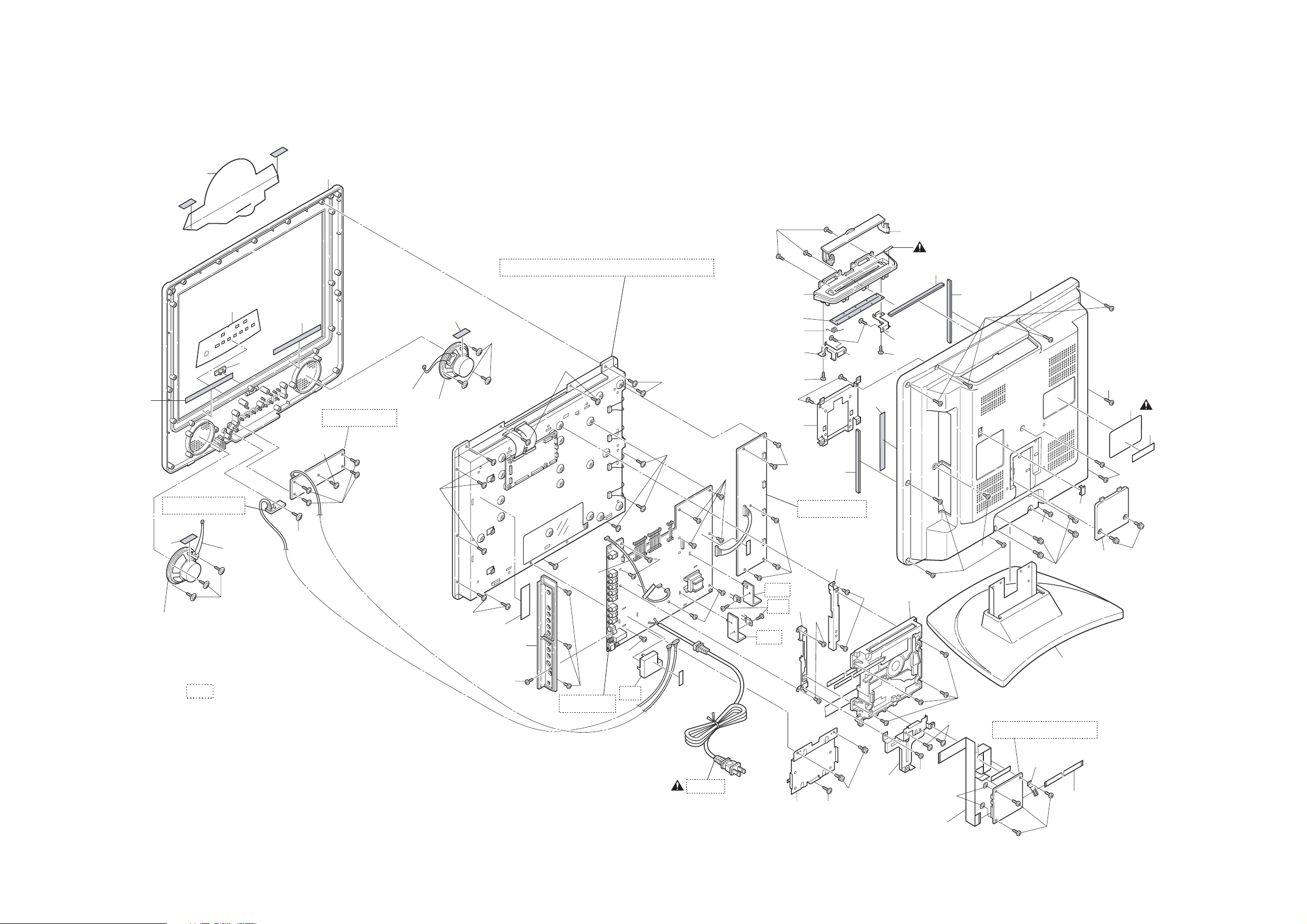
Cabinet
EXPLODED VIEWS
B34
A28
IR Sensor CBA
B5
SP801
A1
A3
B34
A2
Function CBA
L19
L19
CLN801
L19
See Electrical Parts List
for parts with this mark.
L1
CLN802
SP802
L22
B5
L22
LCD Main CBA & Liquid Crystal Panel Unit
L19
L22
B30
L9
B4
L22
CL1651
L21
Main CBA
L21
B7
L21
L22
L22
L21
L21
L23
B10
B22
L4
A14
B28
B27
B32
L14
L23
B3
L21
L21
B25
L23
B21
Inverter CBA
B24
L21
B34
L21
A15
B31
L14
1B1
A16
B21
L2
B21
L2
L3
A4
L2
L2
L17
DVD Main CBA Unit
L7
A9
A10
A8
L2
A6
S5
L2
L6
B33
AC601
B12
15-1 L3250CEX
L1
B26
L7
L3
B17
CL1761
CL1701
L21

Packing
S2
Some Ref. Numbers are
not in sequence.
S3
X2
X3
X1
X4
Tape
S8
S4
Tape
S3
Packing Tape
Packing Tape
Packing Tape
S5
FRONT
S1
15-2 L3250PEX

MECHANICAL PARTS LIST
PRODUCT SAFETY NOTE: Products marked with a
# have special characteristics important to safety.
Before replacing any of these components, read
carefully the product safety notice in this service
manual. Don't degrade the safety of the product
through improper servicing.
NOTE: Parts that are not assigned part numbers
(---------) are not available.
Ref. No. Description Part No.
A1 FRONT CABINET L3250UA 1EM020212
A2 BRAND BADGE L T9000UA~SYLVANIA~ 0EM409016
A3 CONTROL PLATE L3250UA 1EM220221
A4 REAR CABINET L3250UA 1EM020211A
A6# RATING LABEL L3250UA ----------
A8 REAR COVER L3207UH 1EM420953
A9 TILT STAND ASSEMBLY L0301UB 1EMN20039
A10 CONNECTER CAP L3250UA 1EM421023
A14 DVD BASE L3150UA 1EM421054A
A15 DVD DOOR L3150UA 1EM421055
A16# CAUTION LABEL L3150UA ----------
A28 POP SHEET L3150UA 1EM320395
1B1 DVD MECHA (TV-SLOT IN) N7XT0JVM N7XT0JVM
B3 STAND HOLDER L0200UA 0EM301999A
B4 JACK HOLDER L3150UA 1EM320237
B5 CLOTH(10X30XT0.5) B5900UA 0EM404486
B12 TILT STAND HOLDER L3250UA 1EM320239
B17 WASHER(D8) H1600UD 0VM408931
B21 CLOTH(10X180XT0.5) L0336JG 0EM408827
B24 20V DVD HOLDER (R) L3250UA 1EM320234A
B25 20V DVD HOLDER (L) L3250UA 1EM320236A
B26 LOADER PCB HOLDER L3150UA 1EM220261
B27 DVD DOOR SPRING L3150UA 1EM420018A
B28 FELT L3150UA 1EM420406A
B30 LASER CAUTION LABEL L3150UA ----------
B31 BASE HOLDER(L) L3150UA 1EM421403
B32 BASE HOLDER(R) L3150UA 1EM421404
B33 LOADER EARTH PLATE L3150UA 1EM421402
B34 CLOTH 10X150XT1.0 1EM421092
CL1651 14P WIRE ASSEMBLY WX1L3150-005 WX1L3150-005
CL1701 11P FFC CABLE WX1L3250-004 WX1L3250-004
CL1761 25P FFC CABLE WX1L3250-005 WX1L3250-005
CLN801 SPEAKER WIRE ASSEMBLY WX1L3100-001 WX1L3100-001
CLN802 SPEAKER WIRE ASSEMBLY WX1L3100-001 WX1L3100-001
L1 SCREW P-TIGHT 3X12 WASHER HEAD+ GCMP3120
L2 SCREW P-TIGHT 3X12 BIND HEAD+ BLK GBKP3120
L3 SCREW S-TIGHT M3X10 BIND HEAD+ GBMS3100
L6 DOUBLE SEMS SCREW M4X9 L0130UA 0EM408146
L7 DOUBLE SEMS SCREW M4X12 + BLAK FPK34120
L9 SCREW P-TIGHT 3X10 BIND HEAD+ GBKP3100
L14 P-TIGHT SCREW 3X8 BIND + GBMP3080
L17 SCREW S-TIGHT M3X8 BIND HEAD + BLK GBKS3080
L19 ASSEMBLED SCREW M3X10 1EM420633
L21 SCREW S-TIGHT M3X8 BIND HEAD+ GBMS3080
L22 SCREW P-TIGHT 3X14 WASHER HEAD+ GCMP3140
L23 SCREW P-TIGHT M3X8 BIND HEAD+ BLK GBKP3080
SP801 SPEAKER S08F02B DSD0808XQ010
SP802 SPEAKER S08F02B DSD0808XQ010
Ref. No. Description Part No.
PACKING
S1 CARTON L3250UA 1EM420938
S2 STYROFOAM TOP L3250UA 1EM020208
S3 STYROFOAM BOTTOM L3250UA 1EM020210
S4 SET BAG L0301UB 1EM320014
S5 SERIAL NO. LABEL L9750UA ----------
S8 STAND HOLD PAD L3250UA 1EM421522
ACCESSORIES
X1 BAG POLYETHYLENE 235X365XT0.03 0EM408420
X2# OWNERS MANUAL L3250UA 1EMN20477
X3 REMOTE CONTROL 192/ECNLC3D1/
X4 DRY BATTERY R6P/2S XB0M451T0001
NE240UD
NE240UD
20050609 16-1 L3250CA

ELECTRICAL PARTS LIST
PRODUCT SAFETY NOTE: Products marked with a
# have special characteristics important to safety.
Before replacing any of these components, read
carefully the product safety notice in this service
manual. Don't degrade the safety of the product
through improper servicing.
NOTES:
1. Parts that are not assigned part numbers (---------)
are not available.
2. Tolerance of Capacitors and Resistors are noted
with the following symbols.
C.....±0.25% D.....±0.5% F.....±1%
G.....±2% J......±5% K.....±10%
M.....±20% N.....±30% Z.....+80/-20%
DVD MAIN CBA UNIT
Ref. No. Description Part No.
DVD MAIN CBA UNIT N7XT0JUP
LCD MAIN CBA & LIQUID CRYSTAL
PANEL UNIT
Ref. No. Description Part No.
LCD MAIN CBA & LIQUID CRYSTAL PANEL
UNIT
1FSA10059
MMA CBA
Ref. No. Description Part No.
MMA CBA
Consists of the following:
MAIN CBA
IR SENSOR CBA
MAIN CBA
Ref. No. Description Part No.
MAIN CBA
Consists of the following:
CAPACITORS
C11 ELECTROLYTIC CAP. 47µF/10V M CE1AMASDL470
C12 CHIP CERAMIC CAP.(1608) B K 0.01µF/50V CHD1JK30B103
C13 CHIP CERAMIC CAP.(1608) B K 0.01µF/50V CHD1JK30B103
C15 ELECTROLYTIC CAP. 1µF/50V M CE1JMASDL1R0
C21 CHIP CERAMIC CAP.(1608) B K 0.01µF/50V CHD1JK30B103
C22 ELECTROLYTIC CAP. 100µF/10V M CE1AMASDL101
C23 CHIP CERAMIC CAP.(1608) CH J 1000pF/50V CHD1JJ3CH102
C24 CHIP CERAMIC CAP.(1608) CH J 1000pF/50V CHD1JJ3CH102
C25 CHIP CERAMIC CAP.(1608) B K 0.01µF/50V CHD1JK30B103
C26 PCB JUMPER D0.6-P5.0 JW5.0T
C27 FILM CAP.(P) 0.018µF/50V J CA1J183MS029
C28 CHIP CERAMIC CAP.(1608) B K 0.047µF/50V CHD1JK30B473
C29 CHIP CERAMIC CAP. CH D 3pF/50V CHD1JD3CH3R0
C30 CHIP CERAMIC CAP.(1608) B K 0.01µF/50V CHD1JK30B103
C31 PCB JUMPER D0.6-P5.0 JW5.0T
C32 ELECTROLYTIC CAP. 100µF/10V M CE1AMASDL101
1ESA10882
----------
----------
----------
Ref. No. Description Part No.
C34 CHIP CERAMIC CAP.(1608) CH J 47pF/50V CHD1JJ3CH470
C35 ELECTROLYTIC CAP. 1µF/50V M CE1JMASDL1R0
C36 CHIP CERAMIC CAP.(1608) CH J 47pF/50V CHD1JJ3CH470
C37 CHIP CERAMIC CAP. CH J 680pF/50V CHD1JJ3CH681
C39 ELECTROLYTIC CAP. 0.47µF/50V M CE1JMASDLR47
C41 ELECTROLYTIC CAP. 4.7µF/50V M CE1JMASDL4R7
C42 CHIP CERAMIC CAP.(1608) B K 0.01µF/50V CHD1JK30B103
C43 CHIP CERAMIC CAP.(1608) B K 0.01µF/50V CHD1JK30B103
C44 ELECTROLYTIC CAP. 100µF/10V M CE1AMASDL101
C45 CHIP CERAMIC CAP.(1608) B K 0.01µF/50V CHD1JK30B103
C46 ELECTROLYTIC CAP. 47µF/16V M CE1CMASDL470
C501 ELECTROLYTIC CAP. 22µF/50V M H7 CE1JMAVSL220
C502 CHIP CERAMIC CAP.(1608) B K 0.01µF/50V CHD1JK30B103
C503 ELECTROLYTIC CAP. 220µF/16V M CE1CMASDL221
C504 ELECTROLYTIC CAP. 100µF/10V M CE1AMASDL101
C505 CHIP CERAMIC CAP.(1608) B K 0.01µF/50V CHD1JK30B103
C506 CHIP CERAMIC CAP.(1608) B K 0.01µF/50V CHD1JK30B103
C507 CHIP CERAMIC CAP.(1608) B K 0.01µF/50V CHD1JK30B103
C508 CHIP CERAMIC CAP.(1608) B K 0.01µF/50V CHD1JK30B103
C515 CHIP CERAMIC CAP.(1608) B K 0.01µF/50V CHD1JK30B103
C531 ELECTROLYTIC CAP. 330µF/50V M CE1JMZPDL331
C532 CHIP CERAMIC CAP.(1608) B K 0.22µF/25V CHD1EK30B224
C534 ELECTROLYTIC CAP. 47µF/16V M H7 CE1CMAVSL470
C535 ELECTROLYTIC CAP. 470µF/16V M CE1CMASDL471
C537 CHIP CERAMIC CAP.(1608) B K 0.01µF/50V CHD1JK30B103
C538 ELECTROLYTIC CAP. 10µF/50V M CE1JMASDL100
C539 CHIP CERAMIC CAP.(1608) CH J 100pF/50V CHD1JJ3CH101
C601# METALLIZED FILM CAP. 0.22µF/250V CT2E224MS037
C602# METALLIZED FILM CAP. 0.1µF/250V CT2E104MS037
C608 CERAMIC CAP. B K 1000pF/2KV CCD3DKP0B102
C610 ELECTROLYTIC CAP. 150µF/200V M CE2DMZPDL151
C612 FILM CAP.(P) 0.01µF/50V J CMA1JJS00103
C613 FILM CAP.(P) 0.056µF/50V J CMA1JJS00563
C614 PCB JUMPER D0.6-P5.0 JW5.0T
C615 PCB JUMPER D0.6-P5.0 JW5.0T
C631# ELECTROLYTIC CAP. 2200µF/35V M CE1GMZPDL222
C633# ELECTROLYTIC CAP. 220µF/16V M CE1CMASDL221
C635# ELECTROLYTIC CAP. 1000µF/10V M CE1AMASDL102
C636 CHIP CERAMIC CAP.(1608) B K 0.1µF/50V CHD1JK30B104
C637# ELECTROLYTIC CAP. 2200µF/35V M CE1GMZPDL222
C638 CHIP CERAMIC CAP.(1608) B K 0.1µF/50V CHD1JK30B104
C639 ELECTROLYTIC CAP. 1000µF/10V M CE1AMASDL102
C641# SAFETY CAP. 4700pF/250V KX CA2E472MR050
C643 ELECTROLYTIC CAP. 1000µF/10V M CE1AMZPDL102
C644# ELECTROLYTIC CAP. 100µF/50V M CE1JMASTL101
C645# ELECTROLYTIC CAP. 10µF/50V M CE1JMASDL100
C646 FILM CAP.(P) 0.068µF/50V J CMA1JJS00683
C648 ELECTROLYTIC CAP. 1µF/50V M CE1JMASDL1R0
C649 CHIP CERAMIC CAP.(1608) B K 0.01µF/50V CHD1JK30B103
C650 CHIP CERAMIC CAP.(1608) B K 0.01µF/50V CHD1JK30B103
C652# ELECTROLYTIC CAP. 470µF/25V M CE1EMZPDL471
C654# ELECTROLYTIC CAP. 100µF/200V M CE2DMZPDL101
C657 ELECTROLYTIC CAP. 47µF/16V M CE1CMASDL470
C659 FILM CAP.(P) 0.022µF/50V J CMA1JJS00223
C660 FILM CAP.(P) 0.0068µF/50V J CMA1JJS00682
C671 ELECTROLYTIC CAP. 470µF/10V M CE1AMASTL471
C672 CHIP CERAMIC CAP.(1608) B K 0.01µF/50V CHD1JK30B103
C673 ELECTROLYTIC CAP. 470µF/10V M CE1AMASTL471
C674 CHIP CERAMIC CAP.(1608) B K 0.01µF/50V CHD1JK30B103
C701 CHIP CERAMIC CAP.(1608) B K 0.01µF/50V CHD1JK30B103
20050609 17-1 L3250EL

Ref. No. Description Part No.
C702 CHIP CERAMIC CAP.(1608) B K 0.01µF/50V CHD1JK30B103
C703 ELECTROLYTIC CAP. 47µF/16V M H7 CE1CMAVSL470
C704 ELECTROLYTIC CAP. 47µF/16V M H7 CE1CMAVSL470
C705 CHIP CERAMIC CAP.(1608) B K 0.01µF/50V CHD1JK30B103
C706 CHIP CERAMIC CAP.(1608) CH J 1000pF/50V CHD1JJ3CH102
C707 CHIP CERAMIC CAP.(1608) CH J 1000pF/50V CHD1JJ3CH102
C708 CHIP CERAMIC CAP.(1608) CH J 100pF/50V CHD1JJ3CH101
C711 ELECTROLYTIC CAP. 47µF/16V M H7 CE1CMAVSL470
C712 ELECTROLYTIC CAP. 47µF/16V M CE1CMASDL470
C713 CHIP CERAMIC CAP.(1608) B K 3300pF/50V CHD1JK30B332
C714 CHIP CERAMIC CAP. F Z 1µF/10V CHD1AZ30F105
C715 CHIP CERAMIC CAP.(1608) B K 3300pF/50V CHD1JK30B332
C716 CHIP CERAMIC CAP. F Z 1µF/10V CHD1AZ30F105
C722 ELECTROLYTIC CAP. 47µF/16V M CE1CMASDL470
C726 ELECTROLYTIC CAP. 47µF/16V M CE1CMASDL470
C730 ELECTROLYTIC CAP. 47µF/16V M CE1CMASDL470
C734 CHIP CERAMIC CAP.(1608) B K 0.01µF/50V CHD1JK30B103
C735 CHIP CERAMIC CAP.(1608) B K 0.01µF/50V CHD1JK30B103
C736 CHIP CERAMIC CAP.(1608) B K 0.01µF/50V CHD1JK30B103
C738 CHIP CERAMIC CAP.(1608) B K 0.01µF/50V CHD1JK30B103
C739 ELECTROLYTIC CAP. 100µF/10V M H7 CE1AMAVSL101
C740 CHIP CERAMIC CAP.(1608) CH J 100pF/50V CHD1JJ3CH101
C751 CHIP CERAMIC CAP. F Z 1µF/10V CHD1AZ30F105
C752 CHIP CERAMIC CAP. F Z 1µF/10V CHD1AZ30F105
C753 CHIP CERAMIC CAP.(1608) B K 3300pF/50V CHD1JK30B332
C754 CHIP CERAMIC CAP.(1608) B K 3300pF/50V CHD1JK30B332
C781 ELECTROLYTIC CAP. 10µF/50V M H7 CE1JMAVSL100
C782 CHIP CERAMIC CAP.(1608) B K 0.1µF/50V CHD1JK30B104
C784 CHIP CERAMIC CAP.(1608) B K 0.01µF/50V CHD1JK30B103
C785 ELECTROLYTIC CAP. 100µF/10V M H7 CE1AMAVSL101
C787 CHIP CERAMIC CAP.(1608) B K 0.01µF/50V CHD1JK30B103
C801 ELECTROLYTIC CAP. 220µF/16V M CE1CMASDL221
C802 ELECTROLYTIC CAP. 220µF/16V M CE1CMASDL221
C803 FILM CAP.(P) 0.1µF/50V J CMA1JJS00104
C804 FILM CAP.(P) 0.1µF/50V J CMA1JJS00104
C805 ELECTROLYTIC CAP. 10µF/50V M CE1JMASDL100
C806 CHIP CERAMIC CAP. F Z 1µF/10V CHD1AZ30F105
C807 CHIP CERAMIC CAP. F Z 1µF/10V CHD1AZ30F105
C809 ELECTROLYTIC CAP. 2.2µF/50V M CE1JMASDL2R2
C811 ELECTROLYTIC CAP. 100µF/16V M CE1CMASDL101
C812 CHIP CERAMIC CAP. F Z 1µF/10V CHD1AZ30F105
C813 CHIP CERAMIC CAP. F Z 1µF/10V CHD1AZ30F105
C818 ELECTROLYTIC CAP. 2200µF/16V M CE1CMZPDL222
C819 CHIP CERAMIC CAP. B K 2200pF/50V CHD1JK30B222
C820 CHIP CERAMIC CAP. B K 2200pF/50V CHD1JK30B222
C822 ELECTROLYTIC CAP. 10µF/50V M CE1JMASDL100
C823 ELECTROLYTIC CAP. 10µF/50V M CE1JMASDL100
C824 CHIP CERAMIC CAP.(1608) B K 5600pF/50V CHD1JK30B562
C825 CHIP CERAMIC CAP.(1608) B K 5600pF/50V CHD1JK30B562
C826 ELECTROLYTIC CAP. 1µF/50V M CE1JMASDL1R0
C851 CHIP CERAMIC CAP.(1608) CH J 100pF/50V CHD1JJ3CH101
C852 CHIP CERAMIC CAP.(1608) CH J 100pF/50V CHD1JJ3CH101
C853 ELECTROLYTIC CAP. 2.2µF/50V M H7 CE1JMAVSL2R2
C854 CHIP CERAMIC CAP.(1608) B K 0.1µF/50V CHD1JK30B104
C855 CHIP CERAMIC CAP.(1608) B K 0.1µF/50V CHD1JK30B104
C856 CHIP CERAMIC CAP.(1608) B K 0.33µF/10V CHD1AK30B334
C857 ELECTROLYTIC CAP. 2.2µF/50V M H7 CE1JMAVSL2R2
C858 ELECTROLYTIC CAP. 2.2µF/50V M H7 CE1JMAVSL2R2
C859 ELECTROLYTIC CAP. 4.7µF/50V M H7 CE1JMAVSL4R7
C860 ELECTROLYTIC CAP. 10µF/50V M H7 CE1JMAVSL100
C861 ELECTROLYTIC CAP. 100µF/10V M H7 CE1AMAVSL101
C862 CHIP CERAMIC CAP.(1608) B K 0.01µF/50V CHD1JK30B103
C863 ELECTROLYTIC CAP. 2.2µF/50V M H7 CE1JMAVSL2R2
Ref. No. Description Part No.
C864 CHIP CERAMIC CAP.(1608) B K 0.022µF/50V CHD1JK30B223
C865 CHIP CERAMIC CAP.(1608) B K 0.1µF/50V CHD1JK30B104
C866 CHIP CERAMIC CAP. F Z 2.2µF/10V CHD1AZ30F225
C867 CHIP CERAMIC CAP. F Z 2.2µF/10V CHD1AZ30F225
C868 CHIP CERAMIC CAP. B K 1µF/16V CHD1CK30B105
C869 CHIP CERAMIC CAP.(1608) B K 0.022µF/50V CHD1JK30B223
C1652 CHIP CERAMIC CAP.(1608) B K 0.01µF/50V CHD1JK30B103
C1653 ELECTROLYTIC CAP. 100µF/10V M CE1AMASDL101
C1654 CHIP CERAMIC CAP.(1608) B K 0.01µF/50V CHD1JK30B103
C1655 CHIP CERAMIC CAP.(1608) B K 0.01µF/50V CHD1JK30B103
C1656 ELECTROLYTIC CAP. 100µF/10V M CE1AMASDL101
C1657 ELECTROLYTIC CAP. 1000µF/6.3V M CE0KMASDL102
C1658 ELECTROLYTIC CAP. 470µF/6.3V M CE0KMASDL471
C1662 ELECTROLYTIC CAP. 220µF/6.3V M CE0KMASDL221
C1664 ELECTROLYTIC CAP. 100µF/10V M CE1AMASDL101
C1665 CHIP CERAMIC CAP.(1608) B K 0.01µF/50V CHD1JK30B103
C1666 ELECTROLYTIC CAP. 470µF/25V M CE1EMZPDL471
C1667 CHIP CERAMIC CAP.(1608) B K 0.01µF/50V CHD1JK30B103
C1668 ELECTROLYTIC CAP. 10µF/50V M CE1JMASDL100
C1703 CHIP CERAMIC CAP. F Z 1µF/10V CHD1AZ30F105
C1705 ELECTROLYTIC CAP. 47µF/16V M CE1CMASDL470
C1803 PCB JUMPER D0.6-P5.0 JW5.0T
C1804 PCB JUMPER D0.6-P5.0 JW5.0T
C1805 CHIP CERAMIC CAP.(1608) B K 1000pF/50V CHD1JK30B102
C1806 CHIP CERAMIC CAP.(1608) B K 1000pF/50V CHD1JK30B102
CONNECTORS
CN113 PH CONNECTOR (WHITE) TOP 4P B4B-PH-K-
CN411 PH CONNECTOR TOP 11P B11B-PH-K-S(LF) J3PHC11JG017
CN801 STRAIGHT CONNECTOR BASE 00 8283 0212
CN802 STRAIGHT CONNECTOR BASE 00 8283 0212
CN1651 PHD CONNECTOR B14B-PHDSS-B(LF)(SN) J3F5D14JG003
CN1701 FMN CONNECTOR TOP 11P 11FMN-BTRK JCFNG11JG002
CN101A TWG CONNECTOR 09P TWG-P09P-A1 J3TWA09TG001
CN102A TWG CONNECTOR 23P TWG-P23P-A1 J3TWA23TG001
CN103A TWG CONNECTOR 23P TWG-P23P-A1 J3TWA23TG001
S(LF)
00 000
00 000
J3PHC04JG017
J383C02UG002
J383C02UG002
DIODES
D31 SWITCHING DIODE 1SS400 QD1Z001SS400
D501# SWITCHING DIODE 1SS400 QD1Z001SS400
D502 ZENER DIODE MTZJT-7724B QDTB00MTZJ24
D504# SWITCHING DIODE 1SS400 QD1Z001SS400
D505 IC SHUNT REGULATOR KIA431-AT NSZLA0TJY001
D506 SWITCHING DIODE 1SS400 QD1Z001SS400
D507 ZENER DIODE MTZJT-775.6B QDTB0MTZJ5R6
D510 SWITCHING DIODE 1SS400 QD1Z001SS400
D511 SWITCHING DIODE 1SS400 QD1Z001SS400
D512 SWITCHING DIODE 1SS400 QD1Z001SS400
D513 SWITCHING DIODE 1SS400 QD1Z001SS400
D514 SCHOTTKY BARRIER DIODE ERC81-004 QDPZERC81004
D515 CHIP RES.(1608) 1/10W 0 Ω RRXAZR5Z0000
D520 SCHOTTKY BARRIER DIODE 11EQS04 QD4Z011EQS04
D522 SWITCHING DIODE 1SS400 QD1Z001SS400
D523 SCHOTTKY BARRIER DIODE ERC81-004 QDPZERC81004
D527 SCHOTTKY BARRIER DIODE 11EQS04 QD4Z011EQS04
D605# DIODE 1N5397(FORMING B322- NDWZ001N5397
D606# DIODE 1N5397(FORMING B322- NDWZ001N5397
D607# DIODE 1N5397(FORMING B322- NDWZ001N5397
D608# DIODE 1N5397(FORMING B322- NDWZ001N5397
D609 ZENER DIODE MTZJT-775.6B QDTB0MTZJ5R6
D611# ZENER DIODE MTZJT-7722B QDTB00MTZJ22
D612 SWITCHING DIODE 1SS133(T-77) QDTZ001SS133
20050609 17-2 L3250EL

Ref. No. Description Part No.
D613 SWITCHING DIODE 1SS133(T-77) QDTZ001SS133
D615 SWITCHING DIODE 1SS133(T-77) QDTZ001SS133
D616# ZENER DIODE MTZJT-7733B QDTB00MTZJ33
D620 SWITCHING DIODE 1SS133(T-77) QDTZ001SS133
D624# ZENER DIODE MTZJT-7733B QDTB00MTZJ33
D630# SCHOTTKY BARRIER DIODE ERC84-009 QDLZERC84009
D631# DIODE FR154 NDLZ000FR154
D633# SCHOTTKY BARRIER DIODE ERC81-006 QDQZERC81006
D634 SWITCHING DIODE 1SS133(T-77) QDTZ001SS133
D636 SWITCHING DIODE 1SS133(T-77) QDTZ001SS133
D638 SWITCHING DIODE 1SS133(T-77) QDTZ001SS133
D641# ZENER DIODE MTZJT-7733C QDTC00MTZJ33
D642 SWITCHING DIODE 1SS400 QD1Z001SS400
D643 SWITCHING DIODE 1SS400 QD1Z001SS400
D645# DIODE FR154 NDLZ000FR154
D646# DIODE 1ZC43 QDQZ0001ZC43
D647# ZENER DIODE MTZJT-7739B QDTB00MTZJ39
D648# SWITCHING DIODE 1SS400 QD1Z001SS400
D649# IC SHUNT REGULATOR KIA431-AT NSZLA0TJY001
D650 SWITCHING DIODE 1SS400 QD1Z001SS400
D651 SWITCHING DIODE 1SS400 QD1Z001SS400
D652 SWITCHING DIODE 1SS133(T-77) QDTZ001SS133
D653 SWITCHING DIODE 1SS400 QD1Z001SS400
D655# SCHOTTKY BARRIER DIODE YG861S12RSC QDQZYG861S12
D658 SWITCHING DIODE 1SS133(T-77) QDTZ001SS133
D659 SWITCHING DIODE 1SS133(T-77) QDTZ001SS133
D661 RECTIFIER DIODE FR202-B/P NDQZ000FR202
D662 SWITCHING DIODE 1SS400 QD1Z001SS400
D668 SWITCHING DIODE 1SS400 QD1Z001SS400
D672 SWITCHING DIODE 1SS400 QD1Z001SS400
D681 SWITCHING DIODE 1SS133(T-77) QDTZ001SS133
D682 SWITCHING DIODE 1SS133(T-77) QDTZ001SS133
D701 ZENER DIODE MTZJT-778.2B QDTB0MTZJ8R2
D702 ZENER DIODE MTZJT-778.2B QDTB0MTZJ8R2
D703 ZENER DIODE MTZJT-778.2B QDTB0MTZJ8R2
D801 SWITCHING DIODE 1SS400 QD1Z001SS400
D802 SWITCHING DIODE 1SS400 QD1Z001SS400
D803 ZENER DIODE MTZJT-776.2B QDTB0MTZJ6R2
D804 SWITCHING DIODE 1SS400 QD1Z001SS400
D805 SWITCHING DIODE 1SS400 QD1Z001SS400
D810 ZENER DIODE MTZJT-773.3B QDTB0MTZJ3R3
D1651 ZENER DIODE MTZJT-775.6C QDTC0MTZJ5R6
D1652 IC SHUNT REGULATOR KIA431-AT NSZLA0TJY001
D1653 SWITCHING DIODE 1SS400 QD1Z001SS400
D1654 RECTIFIER DIODE ERA15-02 AERA1502****
D1655 SWITCHING DIODE 1SS400 QD1Z001SS400
D1656 ZENER DIODE MTZJT-773.9B QDTB0MTZJ3R9
D1657 IC SHUNT REGULATOR KIA431-AT NSZLA0TJY001
D1658 RECTIFIER DIODE FR202-B/P NDQZ000FR202
D1659 DIODE FR104-B NDLZ000FR104
D1660 SWITCHING DIODE 1SS133(T-77) QDTZ001SS133
D1661 SCHOTTKY BARRIER DIODE 21DQ04 QDQZ0021DQ04
D1664 RECTIFIER DIODE FR202-B/P NDQZ000FR202
D1665 RECTIFIER DIODE FR202-B/P NDQZ000FR202
D1666 RECTIFIER DIODE FR202-B/P NDQZ000FR202
ICS
IC31 IC VIF/SIF M61116FP TF0G QSZBA0SHT034
IC531# IC REGULATOR KA78R08C NSZBA0SF3119
IC533 IC NJM78L05 QSBLA0ZJR034
IC601# PHOTOCOUPLER PS2501-1W QPEW0PS25011
IC671 VOLTAGE REGULATOR KIA7805API NSBBA0SJY011
IC672 VOLTAGE REGULATOR KIA7805API NSBBA0SJY011
Ref. No. Description Part No.
IC781 IC TC4053BF(EL.N) QSZBA0TTS131
IC801 IC AN17812A QSZBA0SMS017
IC851 IC MTS DECORDER AN5832SA-E1 QSZBA0TMS003
IC852 IC SWITCHING TC4052BF(EL) QSZBA0TTS096
IC1652 VOLTAGE REGULATOR PQ070XF01SZH QSZBA0SSH054
COILS
L11 INDUCTOR 47µH-K-5FT LLARKBSTU470
L12 PCB JUMPER D0.6-P5.0 JW5.0T
L13 INDUCTOR 0.47µH-J-26T LLAXJATTUR47
L21 INDUCTOR 100µH-K-5FT LLARKBSTU101
L22 INDUCTOR 150µH-J-26T LLAXJATTU151
L31 INDUCTOR 22µH-K-5FT LLARKBSTU220
L32 INDUCTOR 18µH-J-26T LLAXJATTU180
L601# LINE FILTER 5.0MH 6Y075 LLBG00ZKT004
L701 INDUCTOR 22µH-K-5FT LLARKBSTU220
L781 PCB JUMPER D0.6-P5.0 JW5.0T
L851 PCB JUMPER D0.6-P5.0 JW5.0T
L1701 PCB JUMPER D0.6-P5.0 JW5.0T
TRANSISTORS
Q32 TRANSISTOR 2SA1175(F) QQSF02SA1175
Q501 TRANSISTOR 2SC2785(F) QQSF02SC2785
Q502 TRANSISTOR 2SA1576A T106R QQ1R2SA1576A
Q503 TRANSISTOR 2SC2785(F) QQSF02SC2785
Q505 TRANSISTOR 2SC2120-Y(TE2 F T) QQSY2SC2120F
Q509 TRANSISTOR 2SA1576A T106R QQ1R2SA1576A
Q510 TRANSISTOR 2SA1175(F) QQSF02SA1175
Q511 RES. BUILT-IN TRANSISTOR BA1F4M-T QQSZ00BA1F4M
Q512 TRANSISTOR 2SC2120-O(TE2 F T) QQS02SC2120F
Q513 TRANSISTOR 2SC2785(F) QQSF02SC2785
Q531 TRANSISTOR 2SC2120-O(TE2 F T) QQS02SC2120F
Q601# FET 2SK3869(Q) QFWZ2SK3869Q
Q603# TRANSISTOR 2SC2120-O(TE2 F T) QQS02SC2120F
Q633 TRANSISTOR 2SC4081 T106 Q QQ1Q02SC4081
Q701 TRANSISTOR 2SC4081 T106 Q QQ1Q02SC4081
Q702 TRANSISTOR 2SC4081 T106 Q QQ1Q02SC4081
Q703 TRANSISTOR 2SC4081 T106 Q QQ1Q02SC4081
Q704 TRANSISTOR 2SC4081 T106 Q QQ1Q02SC4081
Q705 TRANSISTOR 2SC4081 T106 Q QQ1Q02SC4081
Q706 TRANSISTOR 2SC2785(F) QQSF02SC2785
Q707 TRANSISTOR 2SC4081 T106 Q QQ1Q02SC4081
Q708 TRANSISTOR 2SC4081 T106 Q QQ1Q02SC4081
Q802 TRANSISTOR 2SC2785(F) QQSF02SC2785
Q803 TRANSISTOR 2SA1175(F) QQSF02SA1175
Q804 TRANSISTOR 2SC2785(F) QQSF02SC2785
Q1651 TRANSISTOR 2SA1175(F) QQSF02SA1175
Q1652 RES. BUILT-IN TRANSISTOR BA1F4M-T QQSZ00BA1F4M
Q1653 TRANSISTOR 2SC2120-O(TE2 F T) QQS02SC2120F
Q1654 TRANSISTOR 2SC2120-O(TE2 F T) QQS02SC2120F
Q1655 RES. BUILT-IN TRANSISTOR BA1F4M-T QQSZ00BA1F4M
Q1656 TRANSISTOR 2SD400(F) QQUF002SD400
Q1657 TRANSISTOR 2SC2785(F) QQSF02SC2785
Q1701 TRANSISTOR 2SC4081 T106 Q QQ1Q02SC4081
RESISTORS
R11 CHIP RES.(1608) 1/10W J 100 Ω RRXAJR5Z0101
R12 CHIP RES.(1608) 1/10W J 100 Ω RRXAJR5Z0101
R15 CHIP RES.(1608) 1/10W J 4.7k Ω RRXAJR5Z0472
R21 CHIP RES.(1608) 1/10W J 270k Ω RRXAJR5Z0274
R23 CHIP RES.(1608) 1/10W J 2.2k Ω RRXAJR5Z0222
R24 CHIP RES.(1608) 1/10W J 820k Ω RRXAJR5Z0824
R34 CHIP RES.(1608) 1/10W 0 Ω RRXAZR5Z0000
R36 CARBON RES. 1/4W J 12k Ω RCX4JATZ0123
R38 CHIP RES.(1608) 1/10W J 100 Ω RRXAJR5Z0101
20050609 17-3 L3250EL

Ref. No. Description Part No.
R40 CHIP RES.(1608) 1/10W J 15k Ω RRXAJR5Z0153
R42 CHIP RES.(1608) 1/10W J 220 Ω RRXAJR5Z0221
R46 CHIP RES.(1608) 1/10W J 1k Ω RRXAJR5Z0102
R48 PCB JUMPER D0.6-P5.0 JW5.0T
R49 CARBON RES. 1/4W J 100 Ω RCX4JATZ0101
R50 CHIP RES.(1608) 1/10W J 1k Ω RRXAJR5Z0102
R52 CHIP RES.(1608) 1/10W J 470 Ω RRXAJR5Z0471
R450 CHIP RES.(1608) 1/10W 0 Ω RRXAZR5Z0000
R451 CHIP RES.(1608) 1/10W 0 Ω RRXAZR5Z0000
R452 CHIP RES.(1608) 1/10W 0 Ω RRXAZR5Z0000
R501 CHIP RES.(1608) 1/10W F 10k Ω RRXAFR5H1002
R502 CHIP RES.(1608) 1/10W 0 Ω RRXAZR5Z0000
R503 CHIP RES.(100PPM) 1/10W F 3k Ω RRXAFR5H3001
R504 CARBON RES. 1/4W J 470 Ω RCX4JATZ0471
R505 CHIP RES.(1608) 1/10W J 2.7k Ω RRXAJR5Z0272
R506 CHIP RES.(1608) 1/10W 0 Ω RRXAZR5Z0000
R508 METAL OXIDE FILM RES. 1W J 4.7k Ω RN01472ZU001
R509 PCB JUMPER D0.6-P5.0 JW5.0T
R510 CHIP RES.(1608) 1/10W J 100k Ω RRXAJR5Z0104
R512 CHIP RES.(1608) 1/10W J 2.2k Ω RRXAJR5Z0222
R514 CHIP RES.(1608) 1/10W J 22k Ω RRXAJR5Z0223
R515 CARBON RES. 1/4W J 22k Ω RCX4JATZ0223
R516 CHIP RES.(1608) 1/10W J 10k Ω RRXAJR5Z0103
R517 CARBON RES. 1/4W J 120 Ω RCX4JATZ0121
R518 CARBON RES. 1/4W J 47k Ω RCX4JATZ0473
R519 CHIP RES.(1608) 1/10W J 100k Ω RRXAJR5Z0104
R520 CHIP RES.(1608) 1/10W J 10k Ω RRXAJR5Z0103
R521 CARBON RES. 1/4W J 100k Ω RCX4JATZ0104
R522 CHIP RES.(1608) 1/10W J 120k Ω RRXAJR5Z0124
R527 CHIP RES.(1608) 1/10W J 3.9k Ω RRXAJR5Z0392
R528 CHIP RES.(1608) 1/10W J 18k Ω RRXAJR5Z0183
R529 CHIP RES.(1608) 1/10W J 47k Ω RRXAJR5Z0473
R531 CARBON RES. 1/4W J 56k Ω RCX4JATZ0563
R532 CHIP RES.(1608) 1/10W J 100 Ω RRXAJR5Z0101
R533 CHIP RES.(1608) 1/10W J 3.3k Ω RRXAJR5Z0332
R535 CHIP RES.(1608) 1/10W J 56k Ω RRXAJR5Z0563
R536 CARBON RES. 1/4W J 33k Ω RCX4JATZ0333
R537 CHIP RES.(1608) 1/10W J 56k Ω RRXAJR5Z0563
R538 CARBON RES. 1/4W J 1 Ω RCX4JATZ01R0
R539 CARBON RES. 1/4W J 10 Ω RCX4JATZ0100
R540 CARBON RES. 1/4W J 100 Ω RCX4JATZ0101
R552 METAL OXIDE FILM RES. 1W J 1 Ω RN011R0ZU001
R601# CEMENT RES. 3W K 1.2 Ω RW031R2PG007
R603 CARBON RES. 1/4W J 390k Ω RCX4JATZ0394
R604 CARBON RES. 1/4W J 390k Ω RCX4JATZ0394
R605 CARBON RES. 1/4W J 390k Ω RCX4JATZ0394
R606 PCB JUMPER D0.6-P5.0 JW5.0T
R607 CARBON RES. 1/4W J 220 Ω RCX4JATZ0221
R608 CARBON RES. 1/4W J 220 Ω RCX4JATZ0221
R609 CARBON RES. 1/4W J 390k Ω RCX4JATZ0394
R610 CARBON RES. 1/4W J 180 Ω RCX4JATZ0181
R613# METAL OXIDE FILM RES. 2W J 0.47 Ω RN02R47ZU001
R620 CARBON RES. 1/4W J 150 Ω RCX4JATZ0151
R621 CARBON RES. 1/4W J 1.2k Ω RCX4JATZ0122
R622 PCB JUMPER D0.6-P5.0 JW5.0T
R623 CARBON RES. 1/4W J 2.2k Ω RCX4JATZ0222
R635# CHIP RES.(1608) 1/10W J 27k Ω RRXAJR5Z0273
R636 PCB JUMPER D0.6-P5.0 JW5.0T
R637# CHIP RES.(1608) 1/10W J 2.2k Ω RRXAJR5Z0222
R638 METAL OXIDE FILM RES. 2W J 1k Ω RN02102ZU001
R642# CHIP RES.(1608) 1/10W J 27k Ω RRXAJR5Z0273
R645 CARBON RES. 1/4W J 22k Ω RCX4JATZ0223
R646 CARBON RES. 1/4W J 1.2k Ω RCX4JATZ0122
Ref. No. Description Part No.
R647 CHIP RES.(1608) 1/10W F 1.8k Ω RRXAFR5H1801
R648# CHIP RES.(1608) 1/10W F 750 Ω RRXAFR5H7500
R650# CHIP RES.(1608) 1/10W F 4.7k Ω RRXAFR5H0472
R652# CHIP RES.(1608) 1/10W F 2.7k Ω RRXAFR5H2701
R653# CHIP RES.(1608) 1/10W F 2.7k Ω RRXAFR5H2701
R654# CHIP RES.(100PPM) 1/10W F 820 Ω RRXAFR5H8200
R655 CARBON RES. 1/4W J 10k Ω RCX4JATZ0103
R656 CHIP RES.(1608) 1/10W J 100k Ω RRXAJR5Z0104
R657 CARBON RES. 1/4W J 390 Ω RCX4JATZ0391
R658 CARBON RES. 1/4W J 470 Ω RCX4JATZ0471
R661# CHIP RES.(100PPM) 1/10W F 4.3k Ω RRXAFR5H4301
R664 CHIP RES.(1608) 1/10W 0 Ω RRXAZR5Z0000
R665# CHIP RES.(1608) 1/10W 0 Ω RRXAZR5Z0000
R666# CHIP RES.(1608) 1/10W F 3.6k Ω RRXAFR5H3601
R667 CARBON RES. 1/4W J 5.6k Ω RCX4JATZ0562
R668 CHIP RES.(1608) 1/10W J 22k Ω RRXAJR5Z0223
R670 CARBON RES. 1/4W J 47 Ω RCX4JATZ0470
R672 PCB JUMPER D0.6-P5.0 JW5.0T
R701 CHIP RES.(1608) 1/10W J 390 Ω RRXAJR5Z0391
R702 CHIP RES.(1608) 1/10W J 390 Ω RRXAJR5Z0391
R703 CHIP RES.(1608) 1/10W J 33k Ω RRXAJR5Z0333
R704 CHIP RES.(1608) 1/10W J 39k Ω RRXAJR5Z0393
R705 CHIP RES.(1608) 1/10W J 33k Ω RRXAJR5Z0333
R706 CHIP RES.(1608) 1/10W J 39k Ω RRXAJR5Z0393
R707 CHIP RES.(1608) 1/10W J 100 Ω RRXAJR5Z0101
R708 CHIP RES.(1608) 1/10W J 10k Ω RRXAJR5Z0103
R709 CHIP RES.(1608) 1/10W J 10k Ω RRXAJR5Z0103
R710 CHIP RES.(1608) 1/10W J 390 Ω RRXAJR5Z0391
R711 CHIP RES.(1608) 1/10W J 33k Ω RRXAJR5Z0333
R712 CHIP RES.(1608) 1/10W J 39k Ω RRXAJR5Z0393
R713 CHIP RES.(1608) 1/10W J 18k Ω RRXAJR5Z0183
R714 CHIP RES.(1608) 1/10W J 18k Ω RRXAJR5Z0183
R715 CHIP RES.(1608) 1/10W J 100 Ω RRXAJR5Z0101
R716 CARBON RES. 1/4W J 100 Ω RCX4JATZ0101
R717 CHIP RES.(1608) 1/10W J 75 Ω RRXAJR5Z0750
R718 CHIP RES.(1608) 1/10W J 10k Ω RRXAJR5Z0103
R719 CHIP RES.(1608) 1/10W J 10k Ω RRXAJR5Z0103
R720 CHIP RES.(1608) 1/10W J 47k Ω RRXAJR5Z0473
R721 CHIP RES.(1608) 1/10W J 47k Ω RRXAJR5Z0473
R722 CHIP RES.(1608) 1/10W J 75 Ω RRXAJR5Z0750
R725 CHIP RES.(1608) 1/10W J 75 Ω RRXAJR5Z0750
R732 CHIP RES.(1608) 1/10W J 390 Ω RRXAJR5Z0391
R733 CHIP RES.(1608) 1/10W J 33k Ω RRXAJR5Z0333
R734 CARBON RES. 1/4W J 100 Ω RCX4JATZ0101
R735 CHIP RES.(1608) 1/10W J 39k Ω RRXAJR5Z0393
R736 CHIP RES.(1608) 1/10W J 75 Ω RRXAJR5Z0750
R738 CARBON RES. 1/4W J 100 Ω RCX4JATZ0101
R739 CHIP RES.(1608) 1/10W J 100 Ω RRXAJR5Z0101
R740 CHIP RES.(1608) 1/10W J 390 Ω RRXAJR5Z0391
R741 CHIP RES.(1608) 1/10W J 390 Ω RRXAJR5Z0391
R742 CHIP RES.(1608) 1/10W J 75 Ω RRXAJR5Z0750
R743 CHIP RES.(1608) 1/10W J 33k Ω RRXAJR5Z0333
R744 CHIP RES.(1608) 1/10W J 75 Ω RRXAJR5Z0750
R747 CHIP RES.(1608) 1/10W J 39k Ω RRXAJR5Z0393
R748 CHIP RES.(1608) 1/10W J 33k Ω RRXAJR5Z0333
R749 CHIP RES.(1608) 1/10W J 39k Ω RRXAJR5Z0393
R752 CHIP RES.(1608) 1/10W J 18k Ω RRXAJR5Z0183
R755 CHIP RES.(1608) 1/10W J 18k Ω RRXAJR5Z0183
R756 CHIP RES.(1608) 1/10W J 10k Ω RRXAJR5Z0103
R757 CHIP RES.(1608) 1/10W J 47k Ω RRXAJR5Z0473
R758 CHIP RES.(1608) 1/10W J 47k Ω RRXAJR5Z0473
R759 CHIP RES.(1608) 1/10W J 10k Ω RRXAJR5Z0103
R782 CHIP RES.(1608) 1/10W J 10k Ω RRXAJR5Z0103
20050609 17-4 L3250EL

Ref. No. Description Part No.
R784 CHIP RES.(1608) 1/10W J 10k Ω RRXAJR5Z0103
R785 CHIP RES.(1608) 1/10W J 10k Ω RRXAJR5Z0103
R786 CHIP RES.(1608) 1/10W J 10k Ω RRXAJR5Z0103
R787 CHIP RES.(1608) 1/10W J 10k Ω RRXAJR5Z0103
R788 CARBON RES. 1/4W J 10k Ω RCX4JATZ0103
R789 CHIP RES.(1608) 1/10W J 10k Ω RRXAJR5Z0103
R790 CHIP RES.(1608) 1/10W J 10k Ω RRXAJR5Z0103
R791 CARBON RES. 1/4W J 10k Ω RCX4JATZ0103
R792 CARBON RES. 1/4W J 10k Ω RCX4JATZ0103
R793 CARBON RES. 1/4W J 10k Ω RCX4JATZ0103
R794 CHIP RES.(1608) 1/10W J 10k Ω RRXAJR5Z0103
R798 CARBON RES. 1/4W J 1k Ω RCX4JATZ0102
R799 CARBON RES. 1/4W J 1k Ω RCX4JATZ0102
R801 CARBON RES. 1/2W J 180 Ω RCX2JZQZ0181
R802 CARBON RES. 1/2W J 180 Ω RCX2JZQZ0181
R803 CHIP RES.(1608) 1/10W J 100 Ω RRXAJR5Z0101
R804 CHIP RES.(1608) 1/10W J 100 Ω RRXAJR5Z0101
R805# METAL OXIDE FILM RES. 2W J 2.2 Ω RN022R2ZU001
R806 CARBON RES. 1/4W J 3.3k Ω RCX4JATZ0332
R807# METAL OXIDE FILM RES. 2W J 2.2 Ω RN022R2ZU001
R808 CHIP RES.(1608) 1/10W J 56k Ω RRXAJR5Z0563
R809 CHIP RES.(1608) 1/10W J 150k Ω RRXAJR5Z0154
R810 CHIP RES.(1608) 1/10W J 10k Ω RRXAJR5Z0103
R811 CHIP RES.(1608) 1/10W J 10k Ω RRXAJR5Z0103
R813 CHIP RES.(1608) 1/10W J 47k Ω RRXAJR5Z0473
R814 CHIP RES.(1608) 1/10W J 2.7k Ω RRXAJR5Z0272
R816 CARBON RES. 1/4W J 2.7k Ω RCX4JATZ0272
R817 CARBON RES. 1/4W J 47k Ω RCX4JATZ0473
R822 CHIP RES.(1608) 1/10W J 22k Ω RRXAJR5Z0223
R823 CHIP RES.(1608) 1/10W J 22k Ω RRXAJR5Z0223
R824 CHIP RES.(1608) 1/10W J 22k Ω RRXAJR5Z0223
R825 CARBON RES. 1/4W J 22k Ω RCX4JATZ0223
R826 CHIP RES.(1608) 1/10W J 22k Ω RRXAJR5Z0223
R827 CHIP RES.(1608) 1/10W J 22k Ω RRXAJR5Z0223
R829 CHIP RES.(1608) 1/10W J 22k Ω RRXAJR5Z0223
R830 CARBON RES. 1/4W J 22k Ω RCX4JATZ0223
R833 CHIP RES.(1608) 1/10W J 22k Ω RRXAJR5Z0223
R834 CHIP RES.(1608) 1/10W J 22k Ω RRXAJR5Z0223
R835 CHIP RES.(1608) 1/10W J 5.6k Ω RRXAJR5Z0562
R836 CHIP RES.(1608) 1/10W J 330 Ω RRXAJR5Z0331
R837 CHIP RES.(1608) 1/10W J 12k Ω RRXAJR5Z0123
R838 CHIP RES.(1608) 1/10W J 12k Ω RRXAJR5Z0123
R839 CHIP RES.(1608) 1/10W J 12k Ω RRXAJR5Z0123
R842 CARBON RES. 1/4W J 22k Ω RCX4JATZ0223
R843 CARBON RES. 1/4W J 22k Ω RCX4JATZ0223
R844 CHIP RES.(1608) 1/10W J 2.2k Ω RRXAJR5Z0222
R851 CHIP RES.(1608) 1/10W J 100 Ω RRXAJR5Z0101
R852 CHIP RES.(1608) 1/10W J 100 Ω RRXAJR5Z0101
R853 CHIP RES.(1608) 1/10W J 3.3k Ω RRXAJR5Z0332
R855 CHIP RES.(1608) 1/10W J 180k Ω RRXAJR5Z0184
R859 CHIP RES.(1608) 1/10W J 10k Ω RRXAJR5Z0103
R860 CHIP RES.(1608) 1/10W J 10k Ω RRXAJR5Z0103
R861 CHIP RES.(1608) 1/10W J 10k Ω RRXAJR5Z0103
R862 CHIP RES.(1608) 1/10W J 22k Ω RRXAJR5Z0223
R863 CHIP RES.(1608) 1/10W J 1k Ω RRXAJR5Z0102
R1631 CARBON RES. 1/4W J 1k Ω RCX4JATZ0102
R1651 CHIP RES.(1608) 1/10W J 47k Ω RRXAJR5Z0473
R1653 CARBON RES. 1/4W J 180 Ω RCX4JATZ0181
R1654 CARBON RES. 1/4W J 22 Ω RCX4JATZ0220
R1655 CARBON RES. 1/4W J 22k Ω RCX4JATZ0223
R1656 CHIP RES.(1608) 1/10W J 22 Ω RRXAJR5Z0220
R1657 CARBON RES. 1/4W J 390 Ω RCX4JATZ0391
R1659 CARBON RES. 1/4W J 10 Ω RCX4JATZ0100
Ref. No. Description Part No.
R1662 CARBON RES. 1/4W J 1.5 Ω RCX4JATZ01R5
R1663 CARBON RES. 1/4W J 1.5 Ω RCX4JATZ01R5
R1664 CHIP RES.(1608) 1/10W F 18k Ω RRXAFR5H1802
R1665 CHIP RES.(1608) 1/10W F 56k Ω RRXAFR5H5602
R1666 PCB JUMPER D0.6-P5.0 JW5.0T
R1667 CHIP RES.(1608) 1/10W J 47k Ω RRXAJR5Z0473
R1668 CHIP RES.(1608) 1/10W J 390 Ω RRXAJR5Z0391
R1670 CHIP RES.(1608) 1/10W F 8.2k Ω RRXAFR5H0822
R1671 CARBON RES. 1/4W J 2.2k Ω RCX4JATZ0222
R1672 CHIP RES.(1608) 1/10W F 220 Ω RRXAFR5H2200
R1673 CHIP RES.(1608) 1/10W F 4.7k Ω RRXAFR5H0472
R1674 CHIP RES. 1/10W F 5.6k Ω RRXAFR5H0562
R1675 CHIP RES.(1608) 1/10W F 15k Ω RRXAFR5H1502
R1677 CARBON RES. 1/4W J 1 Ω RCX4JATZ01R0
R1679 CARBON RES. 1/4W J 1 Ω RCX4JATZ01R0
R1680 CARBON RES. 1/4W J 220 Ω RCX4JATZ0221
R1681 CHIP RES.(1608) 1/10W J 10k Ω RRXAJR5Z0103
R1682 CARBON RES. 1/4W J 820 Ω RCX4JATZ0821
R1683 CARBON RES. 1/4W J 10k Ω RCX4JATZ0103
R1701 CHIP RES.(1608) 1/10W J 160 Ω RRXAJR5Z0161
R1704 CARBON RES. 1/4W J 160 Ω RCX4JATZ0161
R1705 CHIP RES.(1608) 1/10W J 1.8k Ω RRXAJR5Z0182
R1706 CHIP RES.(1608) 1/10W J 2.2k Ω RRXAJR5Z0222
R1707 CHIP RES.(1608) 1/10W J 2.2k Ω RRXAJR5Z0222
R1708 CHIP RES.(1608) 1/10W J 220 Ω RRXAJR5Z0221
R1709 CHIP RES.(1608) 1/10W J 75 Ω RRXAJR5Z0750
R1802 CHIP RES.(1608) 1/10W J 1.8k Ω RRXAJR5Z0182
R1803 CHIP RES.(1608) 1/10W J 1.8k Ω RRXAJR5Z0182
R1805 CHIP RES.(1608) 1/10W J 3.3k Ω RRXAJR5Z0332
R1806 CHIP RES.(1608) 1/10W J 3.3k Ω RRXAJR5Z0332
R1807 CHIP RES.(1608) 1/10W J 1.5k Ω RRXAJR5Z0152
R1808 CHIP RES.(1608) 1/10W J 1.5k Ω RRXAJR5Z0152
MISCELLANEOUS
AC601# AC CORD PB8K9F4110AB057 WAC0172LW020
B7 SHIELD BOX TOP L3201UB 1EM320159
B10 HEAT SINK PKH ASSEMBLY L3201UB 1EM420648
B22 POW HEAT SINK PKG ASSEMBLY L3201UB 1EM420650
BC602 BEAD INDUCTORS FBR07HA121TB-00 LLBF00ZTU021
BC630 PCB JUMPER D0.6-P5.0 JW5.0T
BC631 PCB JUMPER D0.6-P5.0 JW5.0T
BC632 PCB JUMPER D0.6-P5.0 JW5.0T
BC634 PCB JUMPER D0.6-P5.0 JW5.0T
BC636 PCB JUMPER D0.6-P5.0 JW5.0T
BC637 BEAD INDUCTORS FBR07HA121TB-00 LLBF00ZTU021
BC1651 PCB JUMPER D0.6-P5.0 JW5.0T
BC1652 BEAD INDUCTORS FBR07HA121TB-00 LLBF00ZTU021
BC1653 BEAD INDUCTORS FBR07HA121TB-00 LLBF00ZTU021
BC1654 BEAD INDUCTORS FBR07HA121TB-00 LLBF00ZTU021
BC1655 BEAD INDUCTORS FBR07HA121TB-00 LLBF00ZTU021
CF31 CERAMIC FILTER SFSRA4M50CF00-B0 FBB455PMR004
F601 FUSE 4.00A/125V PAGU20CAG402
FH601 FUSE HOLDER MSF-015 XH01Z00LY001
FH602 FUSE HOLDER MSF-015 XH01Z00LY001
GP641# GAP. FNR-G3.10D FAZ000LD6005
JK1701 RCA JACK(ORANGE) MTJ-032-08B-40 FE JXRL010LY128
JK703 RCA JACK(YELLOW) MTJ-032-06B-20 JXRL010LY050
JK704 RCA JACK(WHITE) MTJ-032-06B-22 JXRL010LY052
JK705 RCA JACK(RED) MTJ-032-06A-21 JYRL010LY014
JK706 RCA JACK(GREEN) MTJ-032-06B-25 JXRL010LY054
JK707 RCA JACK(BLUE) MTJ-032-06B-28 JXRL010LY057
JK708 RCA JACK(RED) MTJ-032-06B-21 JXRL010LY051
JK709 RCA JACK(WHITE) MTJ-032-06B-22 JXRL010LY052
20050609 17-5 L3250EL

Ref. No. Description Part No.
JK710 RCA JACK(RED) MTJ-032-06A-21 JYRL010LY014
JK801 MINI JACK MSJ-2000 JYSL010LY003
JK1701 RCA JACK 1P (ORANGE) MTJ-032-06B-23 JXRL010LY053
JS21 CHIP RES.(1608) 1/10W 0 Ω RRXAZR5Z0000
JS524 PCB JUMPER D0.6-P5.0 JW5.0T
JS530 PCB JUMPER D0.6-P15.0 JW15.0T
JS531 PCB JUMPER D0.6-P5.0 JW5.0T
JS821 CHIP RES.(1608) 1/10W 0 Ω RRXAZR5Z0000
JS823 CHIP RES.(1608) 1/10W 0 Ω RRXAZR5Z0000
JS1654 PCB JUMPER D0.6-P16.5 JW16.5T
L4 SCREW B-TIGHT D3X8 BIND HEAD+ GBMB3080
SA601# SURGE ABSORBER 470V+-10PER NVQZ10D471KB
SF11 SAW FILTER SAFHM45M7VAJZ01B03 FBB456PMR012
T601 POWER TRANSFOMER 20V 5742 LTT00CPKT190
TP402 PCB JUMPER D0.6-P10.0 JW10.0T
TP1801 PCB JUMPER D0.6-P7.5 JW7.5T
TP1802 PCB JUMPER D0.6-P7.5 JW7.5T
TP1803 PCB JUMPER D0.6-P7.5 JW7.5T
TP1804 PCB JUMPER D0.6-P5.0 JW5.0T
TP1805 PCB JUMPER D0.6-P7.5 JW7.5T
TP1806 PCB JUMPER D0.6-P7.5 JW7.5T
TU1 TUNER UNIT TEFH9-002A UTUNNTUAL045
IR SENSOR CBA
Ref. No. Description Part No.
IR SENSOR CBA
Consists of the following:
----------
CAPACITOR
C102 ELECTROLYTIC CAP. 47µF/10V M CE1AMASDL470
RESISTORS
R123 CHIP RES.(1608) 1/10W J 68 Ω RRXAJR5Z0680
R124 CHIP RES.(1608) 1/10W J 68 Ω RRXAJR5Z0680
MISCELLANEOUS
CLN105 5P WIRE ASSEMBLY SENSOR WX1L3250-002 WX1L3250-002
RCV102 REMOCON RECEIVE UNIT PIC-37042SR USESJRSKK034
ANALOG INVERTER CBA
Ref. No. Description Part No.
ANALOG INVERTER CBA
Consists of the following:
INVERTER CBA
FUNCTION CBA
INVERTER CBA
Ref. No. Description Part No.
INVERTER CBA
Consists of the following:
CAPACITORS
C401 ELECTROLYTIC CAP. 47µF/35V M CE1GMASDL470
C402 CHIP CERAMIC CAP.(1608) B K 0.1µF/50V CHD1JK30B104
C403 ELECTROLYTIC CAP. 100µF/16V M CE1CMASDL101
C404 CHIP CERAMIC CAP.(1608) B K 0.01µF/50V CHD1JK30B103
C405 CHIP CERAMIC CAP.(1608) B K 0.047µF/50V CHD1JK30B473
C406 CHIP CERAMIC CAP. CH J 220pF/50V CHD1JJ3CH221
C407 CHIP CERAMIC CAP.(1608) B K 6800pF/50V CHD1JK30B682
C408 CHIP CERAMIC CAP.(1608) B K 4700pF/50V CHD1JK30B472
C409 CHIP CERAMIC CAP.(1608) B K 6800pF/50V CHD1JK30B682
C410 CHIP CERAMIC CAP.(1608) B K 4700pF/50V CHD1JK30B472
C412 CHIP CERAMIC CAP.(1608) B K 0.1µF/50V CHD1JK30B104
C413 ELECTROLYTIC CAP. 0.22µF/50V M CE1JMASDLR22
C414 ELECTROLYTIC CAP. 1µF/50V M CE1JMASDL1R0
1ESA10887
----------
----------
----------
Ref. No. Description Part No.
C415 ELECTROLYTIC CAP. 1µF/50V M CE1JMASDL1R0
C416 CHIP CERAMIC CAP.(1608) B K 0.1µF/50V CHD1JK30B104
C420 ELECTROLYTIC CAP. 47µF/35V M CA1G470SP096
C422 CHIP CERAMIC CAP.(1608) B K 0.1µF/50V CHD1JK30B104
C423 ELECTROLYTIC CAP. 47µF/35V M CA1G470SP096
C425 CHIP CERAMIC CAP.(1608) B K 0.1µF/50V CHD1JK30B104
C426 ELECTROLYTIC CAP. 47µF/35V M CA1G470SP096
C428 CHIP CERAMIC CAP.(1608) B K 0.1µF/50V CHD1JK30B104
C429 CHIP CERAMIC CAP. B K 4.7µF/25V CHF1EK30B475
C430 CHIP CERAMIC CAP. B K 4.7µF/25V CHF1EK30B475
C431 CHIP CERAMIC CAP. B K 4.7µF/25V CHF1EK30B475
C432 CHIP CERAMIC CAP. B K 4.7µF/25V CHF1EK30B475
C433 CHIP CERAMIC CAP. B K 4.7µF/25V CHF1EK30B475
C434 CHIP CERAMIC CAP. B K 4.7µF/25V CHF1EK30B475
C440 CHIP CERAMIC CAP.(1608) B K 0.22µF/25V CHD1EK30B224
C441 CHIP CERAMIC CAP.(1608) B K 0.22µF/25V CHD1EK30B224
C442 CHIP CERAMIC CAP.(1608) B K 0.22µF/25V CHD1EK30B224
C450 CHIP CERAMIC CAP.(1608) B K 0.22µF/25V CHD1EK30B224
C451 CHIP CERAMIC CAP.(1608) B K 0.22µF/25V CHD1EK30B224
C452# CERAMIC CAP. SL D 10pF/3KV CCD3FDASL100
C453 CHIP CERAMIC CAP.(1608) B K 0.022µF/50V CHD1JK30B223
C454# CERAMIC CAP. SL D 10pF/3KV CCD3FDASL100
C455 CHIP CERAMIC CAP.(1608) B K 0.022µF/50V CHD1JK30B223
C460 CHIP CERAMIC CAP.(1608) B K 0.22µF/25V CHD1EK30B224
C462# CERAMIC CAP. SL D 10pF/3KV CCD3FDASL100
C463 CHIP CERAMIC CAP.(1608) B K 0.022µF/50V CHD1JK30B223
C464# CERAMIC CAP. SL D 10pF/3KV CCD3FDASL100
C465 CHIP CERAMIC CAP.(1608) B K 0.022µF/50V CHD1JK30B223
C490 CHIP CERAMIC CAP.(1608) B K 0.22µF/25V CHD1EK30B224
C492# CERAMIC CAP. SL D 10pF/3KV CCD3FDASL100
C493 CHIP CERAMIC CAP.(1608) B K 0.022µF/50V CHD1JK30B223
C494# CERAMIC CAP. SL D 10pF/3KV CCD3FDASL100
C495 CHIP CERAMIC CAP.(1608) B K 0.022µF/50V CHD1JK30B223
C496 ELECTROLYTIC CAP. 470µF/35V M(VR) CE1GMZNTL471
C1401 CHIP CERAMIC CAP.(1608) B K 0.22µF/25V CHD1EK30B224
C1403 CHIP CERAMIC CAP.(1608) B K 0.22µF/25V CHD1EK30B224
C1404 CHIP CERAMIC CAP.(1608) B K 0.22µF/25V CHD1EK30B224
C1409 CHIP CERAMIC CAP.(1608) B K 0.22µF/25V CHD1EK30B224
CONNECTORS
CN450 BACK LIGHT CONNECTOR 1717369-1 JB17D02AP001
CN460 BACK LIGHT CONNECTOR 1717369-1 JB17D02AP001
CN490 BACK LIGHT CONNECTOR 1717369-1 JB17D02AP001
DIODES
D401 SWITCHING DIODE 1SS133(T-77) QDTZ001SS133
D402 ZENER DIODE MTZJT-779.1B QDTB0MTZJ9R1
D403 ZENER DIODE MTZJT-7715B QDTB00MTZJ15
D404 ZENER DIODE MTZJT-7715B QDTB00MTZJ15
D405 ZENER DIODE MTZJT-7715B QDTB00MTZJ15
D411 SWITCHING DIODE 1SS133(T-77) QDTZ001SS133
D420 ZENER DIODE MTZJT-779.1B QDTB0MTZJ9R1
D421 SCHOTTKY BARRIER DIODE 11EQS04 QD4Z011EQS04
D422 SCHOTTKY BARRIER DIODE 11EQS04 QD4Z011EQS04
D425 ZENER DIODE MTZJT-779.1B QDTB0MTZJ9R1
D426 SCHOTTKY BARRIER DIODE 11EQS04 QD4Z011EQS04
D427 SCHOTTKY BARRIER DIODE 11EQS04 QD4Z011EQS04
D430 ZENER DIODE MTZJT-779.1B QDTB0MTZJ9R1
D431 SCHOTTKY BARRIER DIODE 11EQS04 QD4Z011EQS04
D432 SCHOTTKY BARRIER DIODE 11EQS04 QD4Z011EQS04
D450 SWITCHING DIODE 1SS400 QD1Z001SS400
D451 SWITCHING DIODE 1SS400 QD1Z001SS400
D452 SWITCHING DIODE 1SS400 QD1Z001SS400
D453 SWITCHING DIODE 1SS400 QD1Z001SS400
20050609 17-6 L3250EL

Ref. No. Description Part No.
D454 SWITCHING DIODE 1SS400 QD1Z001SS400
D455 SWITCHING DIODE 1SS400 QD1Z001SS400
D456 SWITCHING DIODE 1SS400 QD1Z001SS400
D457 SWITCHING DIODE 1SS133(T-77) QDTZ001SS133
D460 SWITCHING DIODE 1SS400 QD1Z001SS400
D461 SWITCHING DIODE 1SS133(T-77) QDTZ001SS133
D464 SWITCHING DIODE 1SS400 QD1Z001SS400
D465 SWITCHING DIODE 1SS133(T-77) QDTZ001SS133
D466 SWITCHING DIODE 1SS133(T-77) QDTZ001SS133
D467 SWITCHING DIODE 1SS133(T-77) QDTZ001SS133
D472 SWITCHING DIODE 1SS133(T-77) QDTZ001SS133
D473 SWITCHING DIODE 1SS133(T-77) QDTZ001SS133
D490 SWITCHING DIODE 1SS133(T-77) QDTZ001SS133
D491 SWITCHING DIODE 1SS133(T-77) QDTZ001SS133
D492 SWITCHING DIODE 1SS400 QD1Z001SS400
D493 SWITCHING DIODE 1SS133(T-77) QDTZ001SS133
D494 SWITCHING DIODE 1SS133(T-77) QDTZ001SS133
D495 SWITCHING DIODE 1SS133(T-77) QDTZ001SS133
D496 SWITCHING DIODE 1SS400 QD1Z001SS400
D497 SWITCHING DIODE 1SS400 QD1Z001SS400
ICS
IC401 IC BD9766FV-E2 QSZBA0TRM062
IC402 IC BA10324AF-E2 QSZBA0TRM032
TRANSISTORS
Q403 TRANSISTOR 2SC2120-O(TE2 F T) QQS02SC2120F
Q411# TRANSISTOR KTC3205-Y-AT/P NQSYKTC3205P
Q412 TRANSISTOR 2SC2785(F) QQSF02SC2785
Q421# FET TPC8405(TE12 L Q) QF2ZTPC8405Q
Q426# FET TPC8405(TE12 L Q) QF2ZTPC8405Q
Q433# FET TPC8405(TE12 L Q) QF2ZTPC8405Q
Q451 TRANSISTOR 2SC4081 T106 Q QQ1Q02SC4081
Q452 TRANSISTOR 2SC4081 T106 Q QQ1Q02SC4081
Q454 TRANSISTOR 2SC4081 T106 Q QQ1Q02SC4081
Q455 TRANSISTOR 2SC4081 T106 Q QQ1Q02SC4081
Q461 TRANSISTOR 2SC4081 T106 Q QQ1Q02SC4081
Q462 TRANSISTOR 2SC4081 T106 Q QQ1Q02SC4081
Q491 TRANSISTOR 2SC4081 T106 Q QQ1Q02SC4081
Q492 TRANSISTOR 2SC4081 T106 Q QQ1Q02SC4081
RESISITORS
R402 CHIP RES.(1608) 1/10W J 10k Ω RRXAJR5Z0103
R404 CHIP RES.(1608) 1/10W J 5.1k Ω RRXAJR5Z0512
R405 CARBON RES. 1/4W J 1k Ω RCX4JATZ0102
R406 CARBON RES. 1/4W J 1k Ω RCX4JATZ0102
R407 METAL RESISITOR 2W J 2.2k Ω RN02222ZU001
R408 METAL RESISITOR 2W J 2.2k Ω RN02222ZU001
R409 CHIP RES.(1608) 1/10W J 10k Ω RRXAJR5Z0103
R411 CHIP RES.(1608) 1/10W J 10k Ω RRXAJR5Z0103
R412 CHIP RES.(1608) 1/10W J 10k Ω RRXAJR5Z0103
R413 CHIP RES.(1608) 1/10W J 68k Ω RRXAJR5Z0683
R414 CHIP RES.(1608) 1/10W 0 Ω RRXAZR5Z0000
R415 CHIP RES.(1608) 1/10W F 2k Ω RRXAFR5H2001
R416 CHIP RES.(1608) 1/10W F 30k Ω RRXAFR5H3002
R417 CHIP RES.(1608) 1/10W J 180k Ω RRXAJR5Z0184
R419 CARBON RES. 1/4W J 100k Ω RCX4JATZ0104
R420 CHIP RES.(1608) 1/10W 0 Ω RRXAZR5Z0000
R421 CHIP RES.(1608) 1/10W J 100k Ω RRXAJR5Z0104
R422 CHIP RES.(1608) 1/10W 0 Ω RRXAZR5Z0000
R423 CHIP RES.(1608) 1/10W J 10k Ω RRXAJR5Z0103
R424 CHIP RES.(1608) 1/10W J 10k Ω RRXAJR5Z0103
R425 CHIP RES.(1608) 1/10W J 220 Ω RRXAJR5Z0221
R426 CHIP RES.(1608) 1/10W J 220 Ω RRXAJR5Z0221
R427 CHIP RES.(1608) 1/10W J 15k Ω RRXAJR5Z0153
Ref. No. Description Part No.
R430 CHIP RES.(1608) 1/10W 0 Ω RRXAZR5Z0000
R432 CHIP RES.(1608) 1/10W J 10k Ω RRXAJR5Z0103
R435 PCB JUMPER D0.6-P5.0 JW5.0T
R437 CHIP RES.(1608) 1/10W J 10k Ω RRXAJR5Z0103
R438 CHIP RES.(1608) 1/10W 0 Ω RRXAZR5Z0000
R440 CHIP RES.(1608) 1/10W 0 Ω RRXAZR5Z0000
R442 CHIP RES.(1608) 1/10W 0 Ω RRXAZR5Z0000
R443 CHIP RES.(1608) 1/10W J 10k Ω RRXAJR5Z0103
R453 CHIP RES.(1608) 1/10W F 15 Ω RRXAFR5H15R0
R454 CHIP RES.(100PPM) 1/10W F 1.0k Ω RRXAFR5H1001
R456 CHIP RES.(1608) 1/10W J 10k Ω RRXAJR5Z0103
R457 CHIP RES.(1608) 1/10W J 680k Ω RRXAJR5Z0684
R458 CARBON RES. 1/4W J 10k Ω RCX4JATZ0103
R459 CHIP RES.(1608) 1/10W J 10k Ω RRXAJR5Z0103
R460 CHIP RES.(100PPM) 1/10W F 620 Ω RRXAFR5H6200
R461 CHIP RES.(1608) 1/10W F 15 Ω RRXAFR5H15R0
R466 CHIP RES.(1608) 1/10W J 10k Ω RRXAJR5Z0103
R467 CHIP RES.(1608) 1/10W J 680k Ω RRXAJR5Z0684
R468 CARBON RES. 1/4W J 10k Ω RCX4JATZ0103
R469 CHIP RES.(1608) 1/10W J 10k Ω RRXAJR5Z0103
R472 CHIP RES.(1608) 1/10W F 47.0 Ω RRXAFR5H47R0
R473 CHIP RES. 1/10W F 270 Ω RRXAFR5H2700
R476 CHIP RES.(1608) 1/10W J 1k Ω RRXAJR5Z0102
R477 CARBON RES. 1/4W J 10k Ω RCX4JATZ0103
R478 CHIP RES.(1608) 1/10W J 1k Ω RRXAJR5Z0102
R479 CARBON RES. 1/4W J 10k Ω RCX4JATZ0103
R480 CHIP RES.(1608) 1/10W J 10k Ω RRXAJR5Z0103
R481 CHIP RES.(1608) 1/10W J 10k Ω RRXAJR5Z0103
R482 CARBON RES. 1/4W J 10k Ω RCX4JATZ0103
R483 CHIP RES.(1608) 1/10W J 10k Ω RRXAJR5Z0103
R485 CHIP RES.(1608) 1/10W J 1k Ω RRXAJR5Z0102
R486 CARBON RES. 1/4W J 10k Ω RCX4JATZ0103
R487 CARBON RES. 1/4W J 1k Ω RCX4JATZ0102
R488 CHIP RES.(1608) 1/10W J 10k Ω RRXAJR5Z0103
R490 CHIP RES.(100PPM) 1/10W F 620 Ω RRXAFR5H6200
R491 CHIP RES.(1608) 1/10W F 15 Ω RRXAFR5H15R0
R492 CHIP RES.(1608) 1/10W F 47.0 Ω RRXAFR5H47R0
R493 CHIP RES. 1/10W F 270 Ω RRXAFR5H2700
R495# CHIP RES.(1608) 1/10W J 1 Ω RRXAJR5Z01R0
R1406 CHIP RES.(1608) 1/10W F 2k Ω RRXAFR5H2001
MISCELLANEOUS
CLN411 11P WIRE ASSEMBLY WX1L3200-003 WX1L3200-003
RL401 POWER RELAY SDT-S-112LMR MRNDC12QN014
T450# INVERTER TRANS ETJV25ZB12AC LTZ00CPMS004
T460# INVERTER TRANS ETJV25ZB12AC LTZ00CPMS004
T490# INVERTER TRANS ETJV25ZB12AC LTZ00CPMS004
FUNCTION CBA
Ref. No. Description Part No.
FUNCTION CBA
Consists of the following:
CAPACITORS
C61 CHIP CERAMIC CAP.(1608) B K 0.01µF/50V CHD1JK30B103
C62 CHIP CERAMIC CAP.(1608) B K 0.01µF/50V CHD1JK30B103
RESISTORS
R61 CHIP RES.(1608) 1/10W J 10k Ω RRXAJR5Z0103
R62 CHIP RES.(1608) 1/10W J 47 Ω RRXAJR5Z0470
R63 CHIP RES.(1608) 1/10W J 1.5k Ω RRXAJR5Z0152
R64 CHIP RES.(1608) 1/10W J 1.5k Ω RRXAJR5Z0152
R65 CHIP RES.(1608) 1/10W J 2.2k Ω RRXAJR5Z0222
R66 CHIP RES.(1608) 1/10W J 2.7k Ω RRXAJR5Z0272
R67 CHIP RES.(1608) 1/10W J 4.7k Ω RRXAJR5Z0472
----------
20050609 17-7 L3250EL

Ref. No. Description Part No.
R68 CHIP RES.(1608) 1/10W J 6.8k Ω RRXAJR5Z0682
R69 CHIP RES.(1608) 1/10W J 10k Ω RRXAJR5Z0103
R70 CHIP RES.(1608) 1/10W J 47 Ω RRXAJR5Z0470
R71 CHIP RES.(1608) 1/10W J 1.5k Ω RRXAJR5Z0152
R72 CHIP RES.(1608) 1/10W J 1.5k Ω RRXAJR5Z0152
R73 CHIP RES.(1608) 1/10W J 2.2k Ω RRXAJR5Z0222
R74 CHIP RES.(1608) 1/10W J 2.7k Ω RRXAJR5Z0272
R75 CHIP RES.(1608) 1/10W J 4.7k Ω RRXAJR5Z0472
SWITCHES
SW61 TACT SWITCH SKQSAB SST0101AL038
SW62 TACT SWITCH SKQSAB SST0101AL038
SW63 TACT SWITCH SKQSAB SST0101AL038
SW64 TACT SWITCH SKQSAB SST0101AL038
SW65 TACT SWITCH SKQSAB SST0101AL038
SW67 TACT SWITCH SKQSAB SST0101AL038
SW71 TACT SWITCH SKQSAB SST0101AL038
SW74 TACT SWITCH SKQSAB SST0101AL038
SW75 TACT SWITCH SKQSAB SST0101AL038
SW76 TACT SWITCH SKQSAB SST0101AL038
MISCELLANEOUS
CLN114 5P-8P WIRE ASSEMBLY WX1L3250-001 WX1L3250-001
20050609 17-8 L3250EL

6620LDF
L3250UA
2005-06-30
 Loading...