

Page 1

X7SPA-L
X7SPA-H
X7SPA-HF
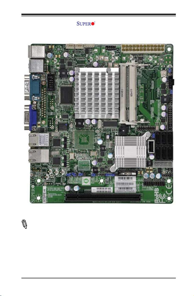
X7SPE-H
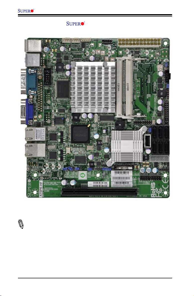
X7SPE-HF
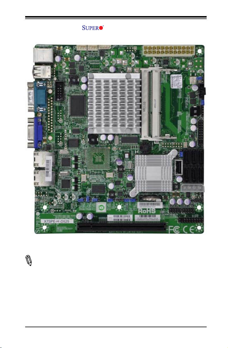
X7SPE-H-D525
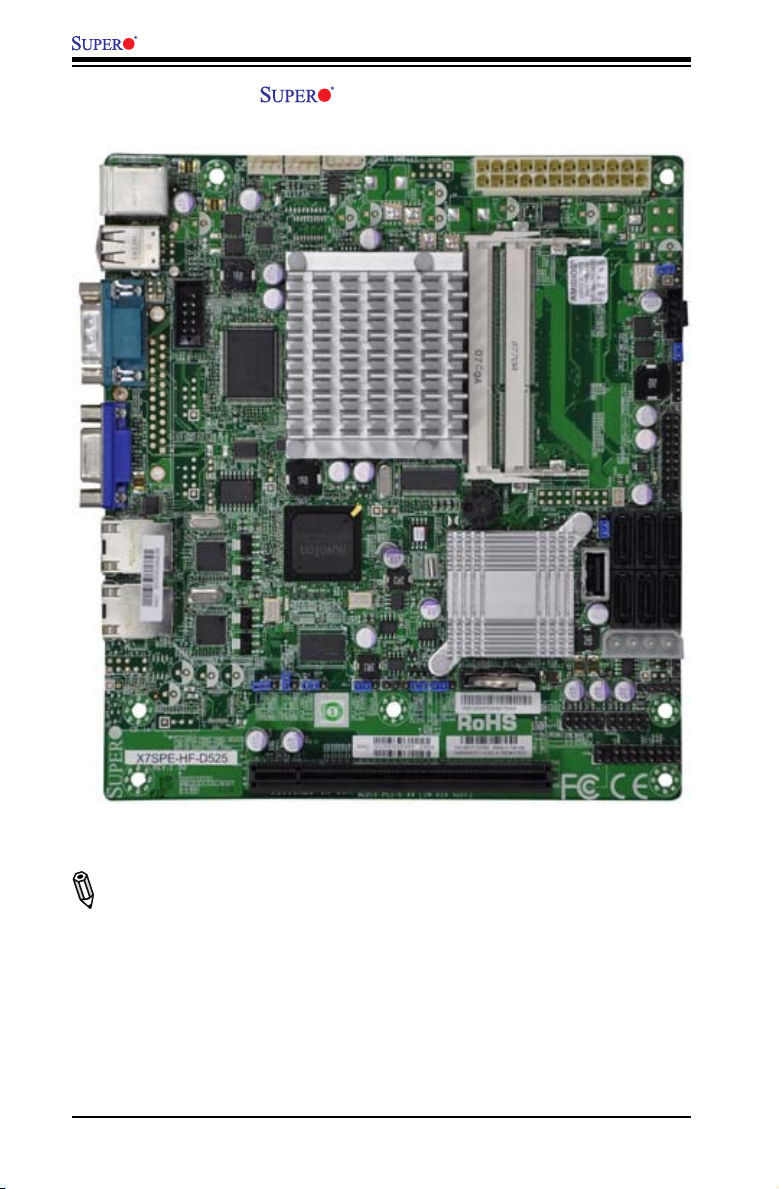
X7SPE-HF-D525
X7SPA-H-D525
X7SPA-HF-D525
USER’S MANUAL
Revision 1.2
Page 2

The information in this User’s Manual has been carefully reviewed and is believed to be accurate.
The vendor assumes no responsibility for any inaccuracies that may be contained in this document,
makes no commitment to update or to keep current the information in this manual, or to notify any
person or organization of the updates. Please Note: For the most up-to-date version of this
manual, please see our web site at www.supermicro.com.
Super Micro Computer, Inc. ("Supermicro") reserves the right to make changes to the product
described in this manual at any time and without notice. This product, including software and documentation, is the property of Supermicro and/or its licensors, and is supplied only under a license.
Any use or reproduction of this product is not allowed, except as expressly permitted by the terms
of said license.
IN NO EVENT WILL SUPER MICRO COMPUTER, INC. BE LIABLE FOR DIRECT, INDIRECT,
SPECIAL, INCIDENTAL, SPECULATIVE OR CONSEQUENTIAL DAMAGES ARISING FROM THE
USE OR INABILITY TO USE THIS PRODUCT OR DOCUMENTATION, EVEN IF ADVISED OF
THE POSSIBILITY OF SUCH DAMAGES. IN PARTICULAR, SUPER MICRO COMPUTER, INC.
SHALL NOT HAVE LIABILITY FOR ANY HARDWARE, SOFTWARE, OR DATA STORED OR USED
WITH THE PRODUCT, INCLUDING THE COSTS OF REPAIRING, REPLACING, INTEGRATING,
INSTALLING OR RECOVERING SUCH HARDWARE, SOFTWARE, OR DATA.
Any disputes arising between manufacturer and customer shall be governed by the laws of Santa
Clara County in the State of California, USA. The State of California, County of Santa Clara shall
be the exclusive venue for the resolution of any such disputes. Supermicro's total liability for all
claims will not exceed the price paid for the hardware product.
FCC Statement: This equipment has been tested and found to comply with the limits for a Class B
digital device pursuant to Part 15 of the FCC Rules. These limits are designed to provide reasonable
protection against harmful interference in a residential installation. This equipment generates,
uses, and can radiate radio frequency energy and, if not installed and used in accordance with the
manufacturer’s instruction manual, may cause interference with radio communications. However,
there is no guarantee that interference will not occur in a particular installation. If this equipment
does cause harmful interference to radio or television reception, which can be determined by
turning the equipment off and on, you are encouraged to try to correct the interference by one
or more of the following measures:
Reorient or relocate the receiving antenna.
Increase the separation between the equipment and the receiver.
Connect the equipment into an outlet on a circuit different from that to which the receiver is
connected.
Consult the dealer or an experienced radio/television technician for help.
California Best Management Practices Regulations for Perchlorate Materials: This Perchlorate
warning applies only to products containing CR (Manganese Dioxide) Lithium coin cells. “Perchlorate
Material-special handling may apply. See www.dtsc.ca.gov/hazardouswaste/perchlorate”.
WARNING: Handling of lead solder materials used in this
product may expose you to lead, a chemical known to
the State of California to cause birth defects and other
reproductive harm.
Manual Revision 1.2
Release Date: December 8, 2010
Unless you request and receive written permission from Super Micro Computer, Inc., you may not
copy any part of this document. Information in this document is subject to change without notice.
Other products and companies referred to herein are trademarks or registered trademarks of their
respective companies or mark holders.
Copyright © 2010-2011 by Super Micro Computer, Inc.
All rights reserved.
Printed in the United States of America
Page 3

Preface
About This Manual
Thi s m a n ual is w r itten f o r s ystem i n t e g r a tors, P C technic i a n s and
knowledgeable PC users. It provides information for the installation and use of the
X7SPA and X7SPE motherboard product series. This product is intended
to be professionally installed and serviced by a technician.
About This Motherboard
The X7SPA and X7SPE motherboard product series are value-driven products
aimed at users who demand a reduced-cost, low-power motherboard for PC or
storage server applications.
The X7SPA and X7SPE series come in different model variations with different
CPU support. The X7SPA-L features a single-core Intel® ATOMTM D410 (1.66GHz,
10.0W) processor, while the X7SPA-H, X7SPA-HF, X7SPE-H, and X7SPE-HF sup-
ports the Intel ATOM D510 (Dual Core, 1.66GHz, 13.0W) processor. In addition,
four other models, the X7SPE-H-D525, X7SPA-HF-D525, X7SPA-H-D525 and the
X7SPE-HF-D525 are equipped with the Intel ATOM D525 (Dual Core, 1.8GHz,
13W) processor. Depending on the particular model, X7SPA and X7SPE series
also offer several conguration choices, including memory up to 4GB (non-ECC
SO-DIMM), up to 6 SATA ports, an on-board VGA, and up to 10 USB 2.0 ports.
These enable the X7SPA and X7SPE series to deliver cost-effective performance
in a small form- factor package.
This wide selection of processors and options make the X7SPA and X7SPE series
an excellent choice for system builders looking to standardize on a particular moth-
erboard line, at cost-effective price points.
Preface
Manual Organization
Chapter 1 describes the features, specications and performance of the mainboard
and provides detailed information about the chipset. Chapter 2 provides hardware
installation instructions. Read this chapter when installing the processor, memory
modules and other hardware components into the system. If you encounter any
problems, see Chapter 3, which describes troubleshooting procedures for video,
memory and system setup stored in the CMOS. Chapter 4 includes an introduction
to the BIOS and provides detailed information on running the CMOS Setup utility.
Appendix A provides BIOS Error Beep Codes. Appendix B lists Driver Installa-
tion Instructions.
iii
Page 4

X7SPA and X7SPE Motherboard Series User’s Manual
Conventions Used in the Manual:
Special attention should be given to the following symbols for proper installation and
to prevent damage done to the components or injury to yourself:
Danger/Caution: Instructions to be strictly followed to prevent catastrophic
system failure or to avoid bodily injury
Warning: Critical information to prevent damage to the components or
data loss.
Important: Important information given to ensure proper system installa-
tion or to relay safety precautions.
Note: Additional Information given to differentiate various models or pro-
vides information for correct system setup.
iv
Page 5

Contacting Supermicro
Headquarters
Address: Super Micro Computer, Inc.
980 Rock Ave.
San Jose, CA 95131 U.S.A.
Tel: +1 (408) 503-8000
Fax: +1 (408) 503-8008
Email: marketing@supermicro.com (General Information)
support@supermicro.com (Technical Support)
Web Site: www.supermicro.com
Europe
Address: Super Micro Computer B.V.
Het Sterrenbeeld 28, 5215 ML
's-Hertogenbosch, The Netherlands
Tel: +31 (0) 73-6400390
Fax: +31 (0) 73-6416525
Email: sales@supermicro.nl (General Information)
support@supermicro.nl (Technical Support)
rma@supermicro.nl (Customer Support)
Contacting Supermicro
Asia-Pacic
Address: Super Micro Computer, Inc.
4F, No. 232-1, Liancheng Rd.
Chung-Ho 235, Taipei County
Taiwan, R.O.C.
Tel: +886-(2) 8226-3990
Fax: +886-(2) 8226-3991
Web Site: www.supermicro.com.tw
Technical Support:
Email: support@supermicro.com.tw
Tel: 886-2-8228-1366, ext.132 or 139
v
Page 6
X7SPA and X7SPE Motherboard Series User’s Manual
Table of Contents
Preface
About This Manual ........................................................................................................iii
About This Motherboard ................................................................................................ iii
Manual Organization .....................................................................................................iii
Conventions Used in the Manual: ................................................................................. iv
Contacting Supermicro ...................................................................................................v
Chapter 1 Introduction
1-1 Overview ......................................................................................................... 1-1
Checklist .......................................................................................................... 1-1
Motherboard Layout (X7SPA-L, X7SPA-H, X7SPA-HF, X7SPA-H-D525,
X7SPA-HF-D525) ...........................................................................................1-11
Motherboard Layout (X7SPE-H, X7SPE-HF, X7SPE-H-D525, X7SPE-
HF-D525) ....................................................................................................... 1-12
X7SPA-L, X7SPA-H, X7SPA-HF, X7SPA-H-D525, X7SPA-HF-D525 Quick
Reference ...................................................................................................... 1-13
X7SPE-H/X7SPE-HF, X7SPE-H-D525, X7SPE-HF-D525, Quick Reference 1-14
Motherboard Features ................................................................................. 1-18
X7SPA/X7SPE Series Block Diagram .......................................................... 1-21
1-2 Chipset Overview ......................................................................................... 1-22
I/O Controller Hub: ICH9R (X7SPA-H/X7SPA-HF, X7SPE-H/X7SPE-HF,
X7SPE-H-D525, X7SPE-HF-D525, X7SPA-H-D525, X7SPA-HF-D525) ...... 1-22
I/O Controller Hub: ICH9 (X7SPA-L) ............................................................. 1-22
1-3 PC Health Monitoring .................................................................................... 1-23
Recovery from AC Power Loss ..................................................................... 1-23
Onboard Voltage Monitoring ........................................................................ 1-23
Fan Status Monitor with Software ................................................................. 1-23
CPU Overheat LED and Control .................................................................. 1-23
1-4 Power Conguration Settings........................................................................ 1-24
X7SPA-L Image ........................................................................... 1-2
X7SPA-H Image .......................................................................... 1-3
X7SPA-HF Image ........................................................................ 1-4
X7SPE-H Image .......................................................................... 1-5
X7SPE-HF Image ......................................................................... 1-6
X7SPE-H-D525 Image ................................................................. 1-7
X7SPE-HF-D525 Image ............................................................... 1-8
X7SPA-H-D525 Image .................................................................. 1-9
X7SPA-HF-D525 Image ............................................................. 1-10
vi
Page 7

Table of Contents
Slow Blinking LED for Suspend-State Indicator ........................................... 1-24
BIOS Support for USB Keyboard.................................................................. 1-24
Main Switch Override Mechanism ................................................................ 1-24
1-5 Power Supply ................................................................................................ 1-24
1-6 Super I/O ....................................................................................................... 1-25
1-7 Overview of the Nuvoton BMC Controller (X7SPA-HF/X7SPE-HF/X7SPE-
HF-D525/X7SPA-HF-D525 only) .............................................................................. 1-25
1-8 LVDS (X7SPA-L only).................................................................................... 1-26
Chapter 2 Installation
2-1 Static-Sensitive Devices .................................................................................. 2-1
Precautions ..................................................................................................... 2-1
Unpacking ....................................................................................................... 2-1
Tools Needed .................................................................................................. 2-2
Location of Mounting Holes ............................................................................ 2-2
2-2 Motherboard Installation .................................................................................. 2-2
Installation Instructions .................................................................................... 2-3
2-3 System Memory .............................................................................................. 2-4
How to Install SO DIMMs ............................................................................... 2-4
Memory Support .............................................................................................. 2-4
The SO DIMM Socket ..................................................................................... 2-5
2-4 Connectors/I/O Ports ....................................................................................... 2-6
Back Panel Connectors and I/O Ports ............................................................ 2-6
ATX PS/2 Keyboard and PS/2 Mouse Ports .............................................. 2-7
Universal Serial Bus (USB) ........................................................................ 2-8
Serial Ports ................................................................................................. 2-9
VGA Connector ........................................................................................ 2-10
LAN Ports / IPMI .......................................................................................2-11
Front Control Panel ....................................................................................... 2-12
JF1 Header Pins ...................................................................................... 2-12
Front Control Panel Pin Denitions............................................................... 2-13
Power LED .............................................................................................. 2-13
HDD LED .................................................................................................. 2-13
NIC1/NIC2 LED Indicators ....................................................................... 2-13
Overheat (OH)/Fan Fail LED.................................................................... 2-14
Power Fail LED ........................................................................................2-14
Reset Button ........................................................................................... 2-15
Power Button ........................................................................................... 2-15
NMI Button .............................................................................................. 2-15
2-5 Connecting Cables ........................................................................................ 2-16
vii
Page 8

X7SPA and X7SPE Motherboard Series User’s Manual
ATX Main PWR & CPU PWR Connectors .............................................. 2-16
External Power Connector ...................................................................... 2-16
Fan Headers ............................................................................................. 2-17
Overheat/Fan Fail LED (JOH) .................................................................. 2-18
Front Panel Audio Header (X7SPA-L Only) ............................................. 2-18
Chassis Intrusion ..................................................................................... 2-19
SATA DOM Power .................................................................................... 2-19
2
Power SMB I
C Connector ...................................................................... 2-19
CD Header (X7SPA-L Only) ..................................................................... 2-20
SMB .......................................................................................................... 2-20
T-SGPIO 0/1 Headers .............................................................................. 2-20
LVDS Connector (X7SPA-L Only) ............................................................ 2-21
Inverter Power Connector (X7SPA-L Only) ........................................ 2-21
TPM Header(X7SPE-H-D525, X7SPE-HF-D525 Only)............................ 2-22
2-6 Jumper Settings ............................................................................................ 2-23
Explanation of Jumpers ............................................................................ 2-23
LAN Port Enable/Disable ......................................................................... 2-24
SMB (I2C) Bus to PCI Slots...................................................................... 2-24
CMOS Clear ............................................................................................. 2-25
USB Wake-Up (Not Available on the X7SPE-H-D525, X7SPA-H-D525,
X7SPA-HF-D525 and X7SPE-HF-D525) .................................................. 2-26
TPM Support Enable (Not available on X7SPA-H-D525, X7SPA-HF-D525,
X7SPE-H-D525, X7SPE-HF-D525) .......................................................... 2-27
Watch Dog Enable/Disable ...................................................................... 2-27
COM3 Redirection Select (OEM Option) .................................................2-27
Power LED/Speaker ................................................................................. 2-28
BMC (X7SPA-HF, X7SPE-HF, X7SPE-HF-D525, X7SPA-H-D525, X7SPA-
HF-D525 Only) ........................................................................................ 2-28
VGA Enable (X7SPA-HF, X7SPE-HF, X7SPE-HF-D525, X7SPA-HF-D525
only) .......................................................................................................... 2-29
HDA/AC97 Select (X7SPA-L Only) ......................................................... 2-29
Power Force On Enable/Disable .............................................................. 2-30
DCD / P5V Select .................................................................................. 2-30
2-7 Onboard Indicators ........................................................................................ 2-31
LAN Port LEDs ......................................................................................... 2-31
2-8 Serial ATA and HDD Connections ................................................................. 2-32
SATA Connectors ..................................................................................... 2-32
viii
Page 9

Table of Contents
Chapter 3 Troubleshooting
3-1 Troubleshooting Procedures ...........................................................................3-1
Before Power On ............................................................................................ 3-1
No Power ........................................................................................................ 3-1
No Video ......................................................................................................... 3-1
Memory Errors ...............................................................................................3-2
Losing the System’s Setup Conguration ....................................................... 3-2
3-2 Technical Support Procedures ........................................................................ 3-2
3-3 Frequently Asked Questions ...........................................................................3-3
3-4 Returning Merchandise for Service................................................................. 3-5
Chapter 4 BIOS
4-1 Introduction ...................................................................................................... 4-1
Starting BIOS Setup Utility .............................................................................. 4-1
How To Change the Conguration Data ......................................................... 4-1
How to Start the Setup Utility ......................................................................... 4-2
4-2 Main Setup ...................................................................................................... 4-2
System Overview: The following BIOS information will be displayed: ....... 4-3
System Time/System Date ........................................................................ 4-3
Processor ................................................................................................... 4-3
System Memory ........................................................................................4-3
4-3 Advanced Setup Congurations...................................................................... 4-4
BOOT Feature .............................................................................................. 4-4
Quick Boot .................................................................................................. 4-4
Quiet Boot .................................................................................................. 4-4
AddOn ROM Display Mode ........................................................................ 4-4
Bootup Num-Lock ....................................................................................... 4-5
PS/2 Mouse Support .................................................................................. 4-5
Wait For 'F1' If Error ................................................................................... 4-5
Hit 'Del' Message Display .......................................................................... 4-5
Watch Dog Function ................................................................................... 4-5
Power Button Function ............................................................................... 4-5
Restore on AC Power Loss ........................................................................ 4-5
Interrupt 19 Capture ................................................................................... 4-5
Standby Power in S5 ................................................................................. 4-6
CPU Conguration ....................................................................................... 4-6
Clock Spread Spectrum .............................................................................4-6
Max CPUID Value Limit.............................................................................. 4-6
ix
Page 10

X7SPA and X7SPE Motherboard Series User’s Manual
Execute-Disable Bit Capability (Available when supported by the OS and
the CPU) ..................................................................................................... 4-6
Hyper-threading Technology ....................................................................... 4-6
Advanced Chipset Control............................................................................ 4-7
Northbridge Conguration ............................................................................ 4-7
DRAM Frequency ....................................................................................... 4-7
Congure DRAM Timing by SPD ............................................................... 4-7
DRAM CAS# Latency ............................................................................... 4-7
DRAM RAS# to CAS# Delay .................................................................... 4-7
DRAM RAS# Precharge ............................................................................. 4-7
DRAM RAS# Activate to Precharge .......................................................... 4-7
Initiate Graphics Adapter ............................................................................ 4-7
Internal Graphics Mode Select ................................................................... 4-7
Video Function Conguration (X7SPA-L, X7SPE-H, X7SPA-H-D525 and
X7SPE-H-D525 only) ...................................................................................... 4-8
DVMT Mode Select .................................................................................... 4-8
DVMT/Fixed Memory ................................................................................. 4-8
Boot Display Device ................................................................................... 4-8
Alternate Video BIOS ................................................................................. 4-8
Active State Power Management ............................................................... 4-8
Reserved Page Route ................................................................................ 4-8
USB Functions ........................................................................................... 4-8
Legacy USB Support (available if USB Functions above is Enabled)....... 4-8
USB Controller ........................................................................................... 4-9
IDE/SATA Conguration ............................................................................... 4-9
SATA#1 Conguration ................................................................................ 4-9
SATA#2 Conguration (Available if IDE is enabled under "Congure
SATA#1 as" above) .................................................................................... 4-9
IDE Detect Timeout (sec) ........................................................................... 4-9
Primary IDE Master/Slave,Secondary IDE Master/Slave,Third IDE
Master,Fourth IDE Master ..........................................................................4-9
PCI/PnP Conguration ...............................................................................4-11
Clear NVRAM ............................................................................................4-11
Plug & Play OS ........................................................................................ 4-12
PCI Latency Timer .................................................................................... 4-12
PCI IDE Bus Master ................................................................................. 4-12
ROM Scan Ordering ................................................................................. 4-12
PCI Slot 1 ................................................................................................. 4-12
Load Onboard LAN 1 Option ROM/ Load Onboard LAN 2 Option ROM 4-12
x
Page 11

Table of Contents
Super IO Device Conguration ................................................................. 4-12
Serial Port1 Address/ Serial Port2 Address ............................................. 4-12
Remote Access Conguration ................................................................... 4-13
Remote Access ....................................................................................... 4-13
Hardware Health Conguration ........................................................ 4-14
CPU Overheat Alarm ................................................................................ 4-14
CPU Temperature ..................................................................................... 4-14
System Temperature ................................................................................ 4-14
CPUFAN / SYSFAN Speed ...................................................................... 4-15
Fan Speed Control Modes ....................................................................... 4-16
CPU Vcore, AVCC, 3.3Vcc, 12V, V_DIMM, 5V, -12V, 3.3Vsb, and Vbat 4-16
ACPI Conguration ..................................................................................... 4-16
High Performance Event Timer ................................................................ 4-16
USB Device Wakeup ................................................................................ 4-16
PS/2 KB/MS WakeUp ............................................................................... 4-16
ACPI Aware O/S ....................................................................................... 4-17
Suspend Mode ......................................................................................... 4-17
AMI OEMB Table ...................................................................................... 4-17
ACPI APIC Support .................................................................................. 4-17
APIC ACPI SCI IRQ ................................................................................. 4-17
Headless Mode ........................................................................................ 4-17
ACPI Version Features ............................................................................. 4-17
IPMI Conguration (X7SPA-HF, X7SPE-HF, X7SPE-HF-D525 & X7SPA-
HF-D525 Only) ............................................................................................. 4-17
IPMI Firmware Revision ........................................................................... 4-17
Status of BMC .......................................................................................... 4-18
IPMI Function ........................................................................................... 4-18
View BMC System Event Log .................................................................. 4-18
Clear BMC System Event Log ................................................................. 4-18
Set LAN Conguration ............................................................................. 4-18
BMC Watch Dog Timer Action ................................................................. 4-19
Event Log Conguration ............................................................................. 4-19
View Event Log ........................................................................................4-19
Mark all events as read ............................................................................ 4-19
Clear event log ......................................................................................... 4-19
PCIE Error Log ......................................................................................... 4-19
4-4 Security Settings ........................................................................................... 4-20
Supervisor Password ..............................................................................4-20
User Password: ........................................................................................ 4-20
xi
Page 12

X7SPA and X7SPE Motherboard Series User’s Manual
Change Supervisor Password .................................................................. 4-20
Change User Password ........................................................................... 4-21
Boot Sector Virus Protection .................................................................... 4-21
4-5 Boot Settings ................................................................................................ 4-22
Boot Device Priority .................................................................................... 4-22
Hard Disk Drives ........................................................................................4-22
Removable Drives ......................................................................................4-23
Retry Boot Devices .................................................................................. 4-23
4-6 Exit Options ................................................................................................... 4-23
Save Changes and Exit ........................................................................... 4-23
Discard Changes and Exit ...................................................................... 4-24
Discard Changes ...................................................................................... 4-24
Load Optimal Defaults .............................................................................. 4-24
Load Fail-Safe Defaults ............................................................................ 4-24
Appendix A POST Error Beep Codes
Recoverable POST Error Beep Codes ......................................................................A-1
Appendix B Software Installation Instructions
B-1 Installing Drivers ..............................................................................................B-1
B-2 Conguring Supero Doctor III .........................................................................B-2
xii
Page 13

Chapter 1: Introduction
Chapter 1
Introduction
1-1 Overview
Checklist
Congratulations on purchasing your computer motherboard from an acknowledged
leader in the industry. Supermicro boards are designed with the utmost attention to
detail and to provide you with the highest standards in quality and performance.
Please check that the following items have all been included with your motherboard.
If anything listed here is damaged or missing, contact your retailer.
All the following items are included in the retail box only.
One (1) Supermicro Mainboard•
Two (2) SATA cables (CBL-0044L)•
One (1) I/O shield (MCP-260-00039-0N) •
One (1) Supermicro CD containing drivers and utilities (CDR-X7-UP)•
One (1) User's/BIOS Manual (MNL-1166)•
1-1
Page 14
X7SPA and X7SPE Motherboard Series User's Manual
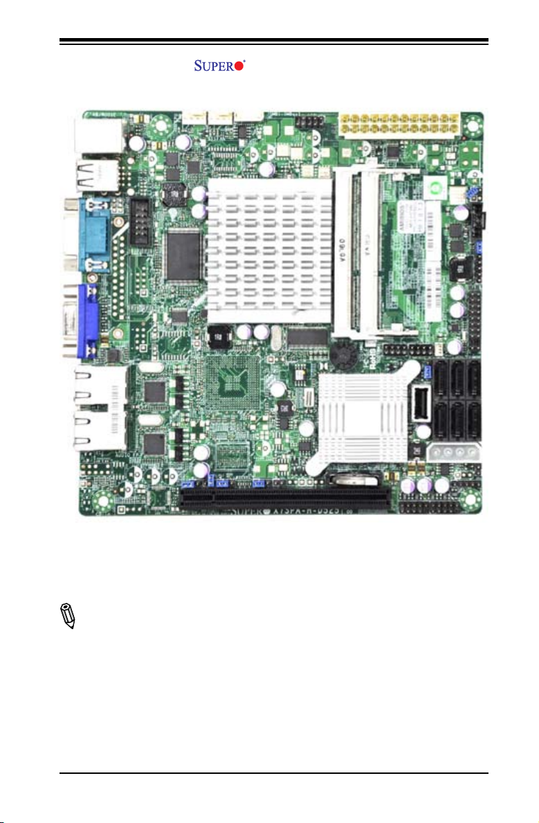
X7SPA-L Image
Note: All graphics and images shown in this manual were based upon the latest
PCB Revision available at the time of publishing of the manual. The motherboard
you've received may or may not look exactly the same as the image shown in
this manual.
1-2
Page 15
X7SPA-H Image
Chapter 1: Introduction
Note: All graphics and images shown in this manual were based upon the latest
PCB Revision available at the time of publishing of the manual. The motherboard
you've received may or may not look exactly the same as the image shown in
this manual.
1-3
Page 16
X7SPA and X7SPE Motherboard Series User's Manual
X7SPA-HF Image
Note: All graphics shown in this manual were based upon the latest PCB Revision
available at the time of publishing of the manual. The motherboard you've received
may or may not look exactly the same as the graphics shown in this manual.
1-4
Page 17
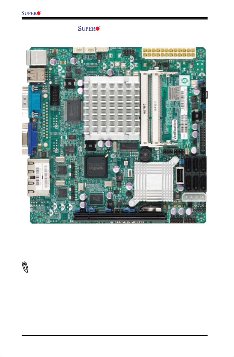
X7SPE-H Image
Chapter 1: Introduction
Note: All graphics shown in this manual were based upon the latest PCB Revision
available at the time of publishing of the manual. The motherboard you've received
may or may not look exactly the same as the graphics shown in this manual.
1-5
Page 18
X7SPA and X7SPE Motherboard Series User's Manual
X7SPE-HF Image
Note: All graphics and images shown in this manual were based upon the latest
PCB Revision available at the time of publishing of the manual. The motherboard
you've received may or may not look exactly the same as the image shown in
this manual.
1-6
Page 19
Chapter 1: Introduction
X7SPE-H-D525 Image
Note: All graphics and images shown in this manual were based upon the latest
PCB Revision available at the time of publishing of the manual. The motherboard
you've received may or may not look exactly the same as the image shown in
this manual.
1-7
Page 20
X7SPA and X7SPE Motherboard Series User's Manual
X7SPE-HF-D525 Image
Note: All graphics and images shown in this manual were based upon the latest
PCB Revision available at the time of publishing of the manual. The motherboard
you've received may or may not look exactly the same as the image shown in
this manual.
1-8
Page 21
Chapter 1: Introduction
X7SPA-H-D525 Image
Note: All graphics and images shown in this manual were based upon the latest
PCB Revision available at the time of publishing of the manual. The motherboard
you've received may or may not look exactly the same as the image shown in
this manual.
1-9
Page 22
X7SPA and X7SPE Motherboard Series User's Manual
X7SPA-HF-D525 Image
Note: All graphics and images shown in this manual were based upon the latest
PCB Revision available at the time of publishing of the manual. The motherboard
you've received may or may not look exactly the same as the image shown in
this manual.
1-10
Page 23
Chapter 1: Introduction
MH2
MH3MH4
D17
JPW1
JUSB1
JD1
JPC3
JPUSB1
JWD1
JPG1
JBMC1
JPL1
JPT1
JPL2
JDIMM2
1
JDIMM1
JI2C2
JI2C1
JOH1
JL1
JL2
SP1
+
J2
J3
JBT1
JBAT1
JPCIE1
JUSB5
JUSB4
JUSB3
JUSB2
JLPC80
R1050
JSMB1
FAN1 FAN2
JCOM2
JCOM4
JPI2C1
JWF1
J8
JVGA1
CD1
JPB
FA N
FAN
COMS CLEAR
2-3 DISABLE
1-2 ENABLE
JPB:BMC ENABLE/DISABLE
CD-in
JPT1:TPM ENABLE/DISABLE
1-2 ENABLE
2-3 DISABLE
AUDIO FP
T-SGPIO2
T-SGPIO1
JPI2C:PWR I2C
JSMB1:SMBus1
JPUSB1:USB WAKE UP
2-3 DISABLE
1-2 ENABLE
JWF1:DOM PWR
JD1:1-3 PWR LED
4-7 SPEAKER
ON:ENABLEJI2C2
OFF:DISABLE
JI2C1
OFF:DISABLE
ON:ENABLE
JL2:AUDIO FRONT PANEL SELECT
ON:AC'97 FRONT PANEL
OFF:HD AUDIO FRONT PANEL
JPG1:VGA
2-3 DISABLE
1-2 ENABLE
2-3 DISABLE
JPL2:1-2 ENABLE
JPL1:1-2 ENABLE
2-3 DISABLE
JL1:CHASISS INTRUSION
JF1 PWR ON RST X OH/FF NIC2 NIC1 HDD LED PWR LED X NMI
2-3 NMI
JWD1:1-2 RST
JBT1:
LAN2
LAN1
I-SATA5
I-SATA2
I-SATA4
I-SATA1
I-SATA3
I-SATA0
SLOT1 PCI-E X4 (IN X16 SLOT)
SYS
CPU
KB/MOUSE
COM4
COM3
COM2
COM1
SODIMM2
SODIMM1
CPU
J6
J5
J10
J11
J12
J13
J14
JPF
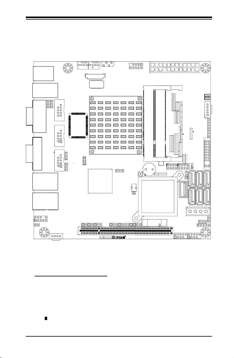
Motherboard Layout (X7SPA-L, X7SPA-H, X7SPA-HF,
X7SPA-H-D525, X7SPA-HF-D525)
1-11
Important Notes to the User
Jumpers not indicated are for testing only. •
See Chapter 2 for detailed information on jumpers, I/O ports and JF1 front •
panel connections.
" " indicates the location of "Pin 1". •
Page 24
X7SPA and X7SPE Motherboard Series User's Manual
MH2
MH3MH4
D17
JPW1
JUSB1
JD1
JWD1
JPG1
JBMC1
JPL1
JPL2
JDIMM2
1
JDIMM1
JI2C2
JI2C1
JOH1
JL1
SP1
+
J2
J3
JBT1
JBAT1
JPCIE1
JUSB5
JUSB4
JUSB3
JUSB2
JLPC80
R1050
JSMB1
FAN1 FAN2
JCOM2
JPI2C1
JWF1
J8
JVGA1
JPB
FA N
FAN
COMS CLEAR
2-3 DISABLE
1-2 ENABLE
JPB:BMC ENABLE/DISABLE
JPT1:TPM ENABLE/DISABLE
1-2 ENABLE
2-3 DISABLE
T-SGPIO2
T-SGPIO1
JPI2C:PWR I2C
JSMB1:SMBus1
JPUSB1:USB WAKE UP
2-3 DISABLE
1-2 ENABLE
JWF1:DOM PWR
JD1:1-3 PWR LED
4-7 SPEAKER
ON:ENABLEJI2C2
OFF:DISABLE
JL2:AUDIO FRONT PANEL SELECT
ON:AC'97 FRONT PANEL
OFF:HD AUDIO FRONT PANEL
JPG1:VGA
2-3 DISABLE
1-2 ENABLE
2-3 DISABLE
JPL2:1-2 ENABLE
JPL1:1-2 ENABLE
2-3 DISABLE
JL1:CHASISS INTRUSION
JF1 PWR ON RST X OH/FF NIC2 NIC1 HDD LED PWR LED X NMI
2-3 NMI
JWD1:1-2 RST
JBT1:
LAN2
LAN1
I-SATA5
I-SATA2
I-SATA4
I-SATA1
I-SATA3
I-SATA0
SYS
CPU
KB/MOUSE
COM2
COM1
SODIMM2
SODIMM1
CPU
JPF
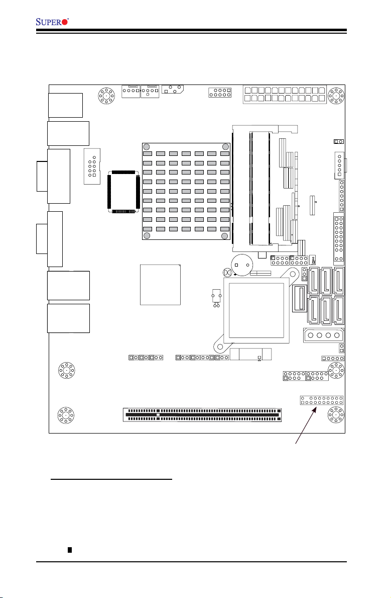
Motherboard Layout (X7SPE-H, X7SPE-HF, X7SPE-H-D525,
X7SPE-HF-D525)
Important Notes to the User
Jumpers not indicated are for testing only. •
See Chapter 2 for detailed information on jumpers, I/O ports and JF1 front •
panel connections.
X7SPE-H-D525 and X7SPE-HF-D525 Only.
" " indicates the location of "Pin 1". •
1-12
Page 25
Chapter 1: Introduction
MH2
MH3MH4
D17
JPW1
JUSB1
JD1
JPC3
JPUSB1
JWD1
JPG1
JBMC1
JPL1
JPT1
JPL2
JDIMM2
1
JDIMM1
JI2C2
JI2C1
JOH1
JL1
JL2
SP1
+
J2
J3
JBT1
JBAT1
JPCIE1
JUSB5
JUSB4
JUSB3
JUSB2
JLPC80
R1050
JSMB1
FAN1 FAN2
JCOM2
JCOM4
JPI2C1
JWF1
J8
JVGA1
CD1
JPB
FA N
FAN
COMS CLEAR
2-3 DISABLE
1-2 ENABLE
JPB:BMC ENABLE/DISABLE
CD-in
JPT1:TPM ENABLE/DISABLE
1-2 ENABLE
2-3 DISABLE
AUDIO FP
T-SGPIO2
T-SGPIO1
JPI2C:PWR I2C
JSMB1:SMBus1
JPUSB1:USB WAKE UP
2-3 DISABLE
1-2 ENABLE
JWF1:DOM PWR
JD1:1-3 PWR LED
4-7 SPEAKER
ON:ENABLEJI2C2
OFF:DISABLE
JI2C1
OFF:DISABLE
ON:ENABLE
JL2:AUDIO FRONT PANEL SELECT
ON:AC'97 FRONT PANEL
OFF:HD AUDIO FRONT PANEL
JPG1:VGA
2-3 DISABLE
1-2 ENABLE
2-3 DISABLE
JPL2:1-2 ENABLE
JPL1:1-2 ENABLE
2-3 DISABLE
JL1:CHASISS INTRUSION
JF1 PWR ON RST X OH/FF NIC2 NIC1 HDD LED PWR LED X NMI
2-3 NMI
JWD1:1-2 RST
JBT1:
LAN2
LAN1
I-SATA5
I-SATA2
I-SATA4
I-SATA1
I-SATA3
I-SATA0
SLOT1 PCI-E X4 (IN X16 SLOT)
SYS
CPU
KB/MOUSE
COM4
COM3
COM2
COM1
SODIMM2
SODIMM1
CPU
J6
J5
J10
J11
J12
J13
J14
JPF
X7SPA-L, X7SPA-H, X7SPA-HF, X7SPA-H-D525, X7SPA-
HF-D525 Quick Reference
(not drawn to scale)
38
37
1
1
343536
1
43
14
49
48
47
46
15
50
44
16
45
17
18
19
52
53
33
32
31
30
29
28
27
26
25
22
24
23
20 21
2
39
1
3
4
40
1
5
11
42
13
12
6
41
7
8
9
Note 1: USB 3/4, COM3/4 are available on the X7SPA-L only. LAN2 and
SATA 2/3 are available on the X7SPA-H, X7SPA-HF, X7SPE-H, X7SPE-
HF, X7SPA-H-D525, X7SPA-HF-D525, X7SPE-H-D525 and X7SPE-HF-
D525 only.
Note 2: Jumpers that are not indicated are used for factory testing only.
10
1-13
Page 26
X7SPA and X7SPE Motherboard Series User's Manual
MH2
MH3MH4
D17
JPW1
JUSB1
JD1
JWD1
JPG1
JBMC1
JPL1
JPL2
JDIMM2
1
JDIMM1
JI2C2
JI2C1
JOH1
JL1
SP1
+
J2
J3
JBT1
JBAT1
JPCIE1
JUSB5
JUSB4
JUSB3
JUSB2
JLPC80
R1050
JSMB1
FAN1 FAN2
JCOM2
JPI2C1
JWF1
J8
JVGA1
JPB
FA N
FAN
COMS CLEAR
2-3 DISABLE
1-2 ENABLE
JPB:BMC ENABLE/DISABLE
JPT1:TPM ENABLE/DISABLE
1-2 ENABLE
2-3 DISABLE
T-SGPIO2
T-SGPIO1
JPI2C:PWR I2C
JSMB1:SMBus1
JPUSB1:USB WAKE UP
2-3 DISABLE
1-2 ENABLE
JWF1:DOM PWR
JD1:1-3 PWR LED
4-7 SPEAKER
ON:ENABLEJI2C2
OFF:DISABLE
JL2:AUDIO FRONT PANEL SELECT
ON:AC'97 FRONT PANEL
OFF:HD AUDIO FRONT PANEL
JPG1:VGA
2-3 DISABLE
1-2 ENABLE
2-3 DISABLE
JPL2:1-2 ENABLE
JPL1:1-2 ENABLE
2-3 DISABLE
JL1:CHASISS INTRUSION
JF1 PWR ON RST X OH/FF NIC2 NIC1 HDD LED PWR LED X NMI
2-3 NMI
JWD1:1-2 RST
JBT1:
LAN2
LAN1
I-SATA5
I-SATA2
I-SATA4
I-SATA1
I-SATA3
I-SATA0
SYS
CPU
KB/MOUSE
COM2
COM1
SODIMM2
SODIMM1
CPU
JPF
X7SPE-H/X7SPE-HF, X7SPE-H-D525, X7SPE-HF-D525,
Quick Reference
38
37
1
1
343536
1
2
39
1
50
52
3
33
4
32
5
45
44
31
30
29
28
6
27
7
11
12
14
16
13
15
17
Note 1: USB 3/4, COM3/4 are available on the X7SPA-L only. LAN2 and
SATA 2/3 are available on the X7SPA-H, X7SPA-HF, X7SPE-H, X7SPE-
HF, X7SPA-H-D525, X7SPA-HF-D525, X7SPE-H-D525 and X7SPE-HF-
D525 only.
Note 2: Jumpers that are not indicated are used for factory testing only.
18
26
25
22
20
23
21
19
1-14
Page 27
Chapter 1: Introduction
Ports and Connectors
Number Connectors Description
1 KB/Mouse PS/2 Keyboard/Mouse
2, 3 USB 1/2, USB 3/4 Back Panel USB Ports (USB 3/4: X7SPA-L only)
4 COM1 Back Panel Serial Port
5 VGA
Video/Graphics Connector
6 LAN1 RJ45 Connector for LAN1
7 LAN2 RJ45 Connector for LAN2 (Not available on the X7SPA-L)
8 J5
10 CD1
Front Panel Audio Header Connector (Not available on the X7SPE
series)
CD/DVD Drive Audio Input Header (Not available on the X7SPE
series)
15 JL1 Chassis Intrusion Header
18 JBAT1 Onboard Battery
19 JPCIE1
PCI-E 1.1 x4 Gen1 (in x16 physical) Slot 7 (Slot 6 on X7SPE
series)
20 USB 5/6, 7/8 Front Panel USB headers
21 JTPM TPM Header (X7SPE-H-D525/X7SPE-HF-D525 Only)
22 USB 10 Type A on-board USB Port
23 USB 9 Front Panel USB header
25 JOH Overheat Warning LED header
26 J8
Power Connector for Add-on devices (Note: Do NOT plug the
power supply into this socket).
27 SATA 0,1,2,3,4,5 SATA Connectors (SATA 2/3 is not available on the X7SPA-L)
29 JWF1 SATA Disk on Module (DOM) Power
30 T-SGPIO-0/1 Serial General Purpose IO headers (for SATA)
31 JF1 FP Control Panel Header
32 JD1
33 JPI2C PWR supply (I
External Buzzer/Speaker/Power LED
Pins 1-3 (Power LED), Pins 4-7 (External Speaker)
2
C) System Management Bus
34 JPW1 ATX 24-Pin Power Connector
35 Unused Factory Test Point
36 JSMB1 System Management Bus header
38, 37 Fans 1, 2 Fan 1: CPU Fan, Fan 2: Chassis Fan Header
39, 40, 41
COM2, COM4,
COM3
Serial Port 2, 4 and 3 Headers (COM 3/4 X7SPA-L only)
45 SPK Onboard Speaker/Buzzer
48 J5 18-bpp LVDS LCD Monitor Port
49 J6 Inverter Connector
50 DIMM 1, DIMM 2 SO-DIMM Memory Slots
1-15
Page 28
X7SPA and X7SPE Motherboard Series User's Manual
Jumper Descriptions
Number Jumper Description Default Setting
9 JL2
12, 11 JI
AC97/HD Audio Selector
(Front Panel)
2
C1/JI2C2 SMB to PCI Slots Open/Open (Disabled)
Open (HD Audio)
Closed (AC97)
13 JPL2 LAN2 Enable/Disable Pins 1-2 (Enabled)
14 JPL1 LAN1 Enable/Disable Pins 1-2 (Enabled)
Pins 1-2 (Enabled, use
on-board VGA device)
Pins 2-3 (Disabled, use
add-on VGA card)
Pins 1-2 (Enabled)
Pins 2-3 (Disabled)
16 JPG1
17 JPB
On-board VGA Enable/Disable
(X7SPA-HF, X7SPE-HF and X7SPEHF-D525 only)
BMC Enable/Disable (X7SPA-HF,
X7SPE-HF, and X7SPE-HF-D525 only)
24 JPUSB1 USB Wake-up Enable Pins 1-2 (Enabled)
28 JWD1 Watch Dog Timer
42 JPT1 Trusted Platform Module Enable
COM3 Selection (OEM option for the
43 JPC3
X7SPA-H, X7SPA-HF and X7SPE
series)
Pins 1-2 (Reset)
Pins 1-2 (Enabled)
Pins 2-3 (Disabled)
Pins 1-2 (RS232)
Pins 2-3 (TTL)
44 JBT1 CMOS Clear (See Chapter 2)
46 J12/J13
47 J10/J11
Pin 1 DCD/P5V Select (COM3/COM4)
(OEM option for the X7SPA-H, X7SPA-
HF, and X7SPE series)
Pin 1 DCD/P5V Select (COM1/COM2)
(OEM option for the X7SPA-H, X7SPA-
HF, and X7SPE series)
Pins 1-2 (DCD )
Pins 2-3 (P5V)
Pins 1-2 (DCD)
Pins 2-3 (P5V)
52 JPF Power Force On Open (Disabled)
53 J14 Reserved (Unused) Reserved (Unused)
1-16
Page 29
Chapter 1: Introduction
Features
Model CPU Chipset VGA Graphics
X7SPA-L Intel ATOM D410 Intel ICH9 Intel Graphics Media Accelerator GMA3150
X7SPA-H Intel ATOM D510 Intel ICH9R Intel Graphics Media Accelerator GMA3150
X7SPA-HF Intel ATOM D510 Intel ICH9R Matrox G200eW Graphics Accelerator
X7SPE-H Intel ATOM D510 Intel ICH9R Intel Graphics Media Accelerator GMA3150
X7SPE-HF Intel ATOM D510 Intel ICH9R Matrox G200eW Graphics Accelerator
X7SPE-H-D525 Intel ATOM D525 Intel ICH9R Intel Graphics Media Accelerator GMA3150
X7SPE-HF-D525 Intel ATOM D525 Intel ICH9R Matrox G200eW Graphics Accelerator
X7SPA-H-D525 Intel ATOM D525 Intel ICH9R Intel Graphics Media Accelerator GMA3150
X7SPA-HF-D525 Intel ATOM D525 Intel ICH9R Matrox G200eW Graphics Accelerator
Model USB Serial LAN Audio LVDS SATA IPMI RAID TPM
X7SPA-L
X7SPA-H
X7SPAHF
X7SPE-H
X7SPEHF
X7SPEH-D525
X7SPEHF-D525
X7SPA-HD525
X7SPAHF-D525
4 (rear)
1 (type A)
5 (header)
2 (rear)
1 (type A)
5 (header)
2 (rear)
1 (type A)
5 (header)
2 (rear)
1 (type A)
5 (header)
2 (rear)
1 (type A)
5 (header
2 (rear)
1 (type A)
5 (header)
2 (rear)
1 (type A)
5 (header)
2 (rear)
1 (type A)
5 (header)
2 (rear)
1 (type A)
5 (header)
1 (rear)
3 (header)
1 (rear)
1 (header)
1 (rear)
1 (header)
1 (rear)
1 (header)
1 (rear)
1 (header)
1 (rear)
1 (header)
1 (rear)
1 (header)
1 (rear)
1 (header)
1 (rear)
1 (header)
Front
LAN1
Panel
Header
LAN1/
None None 6 No
LAN2
LAN1/
None None 6
LAN2
LAN1/
None None 6 No
LAN2
LAN1/
None None 6
LAN2
LAN1/
None None 6 No
LAN2
LAN1/
None None 6
LAN2
LAN1/
None None 6 No
LAN2
LAN1/
None None 6
LAN2
1 4 No No No
Windows
(0,1,5,10)
Linux
(0,1,10)
Yes
(shared on
LAN1)
Yes
(shared on
LAN1)
Yes
(shared on
LAN1)
Yes
(shared on
LAN1)
Windows
(0,1,5,10)
Linux
(0,1,10)
Windows
(0,1,5,10)
Linux
(0,1,10)
Windows
(0,1,5,10)
Linux
(0,1,10)
Windows
(0,1,5,10)
Linux
(0,1,10)
Windows
(0,1,5,10)
Linux
(0,1,10)
Windows
(0,1,5,10)
Linux
(0,1,10)
Windows
(0,1,5,10)
Linux
(0,1,10)
No
No
No
No
Yes
Yes
No
No
1-17
Page 30
X7SPA and X7SPE Motherboard Series User's Manual
Motherboard Features
Processor
X7SPA-L
Single Integrated Intel® ATOM™ D410 processor, 1.66 GHz, 10 Watts, 512KB
L2 cache, Single Core, Dual Threads.
X7SPA-H, X7SPA-HF, X7SPE-H, X7SPE-HF
Single Integrated Dual-Core Intel® ATOM™ D510 processor, 1.66 GHz, 13
Watts, 2 x 512KB L2 cache, Dual Core, 4 Threads.
X7SPE-H-D525, X7SPE-HF-D525, X7SPA-H-D525, X7SPA-HF-D525
Single Integrated Dual-Core Intel® ATOM™ D525 processor, 1.8 GHz, 13
Watts, 2 x 512KB L2 cache, Dual Core, 4 Threads.
Memory
X7SPA-L, X7SPA-H, X7SPA-HF, X7SPE-H, X7SPE-HF
Supports up to 4GB of unbuffered 667/800 MHz Non-ECC DDR2 SO-DIMMs
in 2 sockets (1.8V, 256MB, 512MB, 1GB, 2GB)
X7SPE-H-D525, X7SPE-HF-D525, X7SPA-HF-D525, X7SPA-H-D525
Supports up to 4GB of unbuffered 800 MHz Non-ECC DDR3 SO-DIMMs in
2 sockets (1.5V, 256MB, 512MB, 1GB, 2GB)
Note: 1666 MHz and 1333 MHz memory may be used, but will operate at
800 MHz.
Chipset
X7SPA-L Only
Intel® ICH9
X7SPA & X7SPE Series
Intel® ICH9R
Integrated Graphics
X7SPA-L, X7SPA-H, X7SPE-H, X7SPE-H-D525, X7SPA-H-D525
Intel Graphics Media Accelerator GMA3150
X7SPA-HF, X7SPE-HF, X7SPE-HF-D525, X7SPA-HF-D525
Matrox G200eW Graphics Accelerator
Expansion Slots
One (1) PCI-E 1.1 x4 Gen1 (in x16 physical) slot•
BIOS
32 Mb AMI BIOS•
®
, SPI Flash BIOS
1-18
Page 31

Chapter 1: Introduction
PC Health Monitoring
Onboard voltage monitors for CPU Cores, Chipset Voltage, Memory Voltage •
+1.8V, +3.3V, +5V, +/- 12V, +3.3V standby, +5V standby, VBat, HT
Tachometer monitoring •
Status monitor for speed control, on/off control•
Supports 3-pin fans (w/o speed control)•
Low-noise fan speed control•
Temperature monitor for chassis, CPU environments•
CPU thermal trip support•
Supero Doctor III, Watch Dog/NMI•
CPU/System overheat LED, Suspend state LED•
PowerConguration
ACPI/ACPM Power Management
•
Wake-On-Ring, Wake-On-LAN headers•
Keyboard wake-up from soft off•
CPU fan auto-off in sleep mode•
Power on mode for AC power recovery•
I/O Controllers and Ports
Built-in ICH9/9R SATA Controller •
Winbond Super I/O controller 83627DHG-P •
One PS/2 mouse and one PS/2 keyboard port•
One back panel VGA port•
X7SPA-L Only
4 SATA connectors for 4 devices•
Single 10/100/1000 LAN (Intel 82574L)•
Four Fast 16550-compatible UART serial ports (one on back panel, three •
internal headers)
Realtek ALC888-VC2-GR HD Audio•
Ten (10) USB 2.0 ports & headers (USB1~USB10): Four ports on the back •
panel, ve USB headers for front panel access, and one on-board Type A
USB port.
Front panel HD audio header, 18-bpp LVDS connector•
Optimized for the Supermicro 1U SC512 & SC731 chassis.•
1-19
Page 32

X7SPA and X7SPE Motherboard Series User's Manual
X7SPA-H/X7SPE-H/X7SPE-H-D525/X7SPA-H-D525 Only
6 SATA connectors for 6 devices •
RAID support: RAID 0, 1, 5, 10 (Windows OS), RAID 0, 1, 10 (Linux OS)•
Dual 10/100/1000 LAN (Intel 82574L)•
Two Fast UART 16550-compatible serial ports (one back panel, one •
header)
Eight (8) USB 2.0 ports & headers (USB1/2, USB5~10): Two ports on the •
back panel, ve USB headers for front panel access, and one on-board
Type A USB port.
Optimized for the Supermicro 1U (502, 503, 510, 512) & SC731 chassis.•
20-pin TPM header (X7SPE-H-D525 only)•
X7SPA-HF/X7SPE-HF/X7SPE-HF-D525, X7SPA-HF-D525 Only
All the features of the X7SPA-H/X7SPE-H/X7SPE-H-D525/X7SPA-H-D525•
Nuvoton WPCM450 BMC (Integrated IPMI 2.0, shared with LAN1)•
Other
Chassis Intrusion Header and Detection
•
Lead free•
CD Utilities
BIOS ash upgrade utility, Drivers and utilities for Intel® ICH9/9R chipset
•
Dimensions
Mini ITX form factor, 6.75" x 6.75" (X7SPA Series)•
Flex ITX form factor, 7.5" x 6.75" (X7SPE Series) •
1-20
Page 33

Chapter 1: Introduction
*SC/DC
Intel ATOM
SODIMM 1
SODIMM 2
DDR2 667
VGA
LVDS
Connector
Connector
Intel
ICH9: X7SPA-L
ICH9R: X7SPA-H,
X7SPA-HF, X7SPE-H,
X7SPE-HF, X7SPE-H-D525,
X7SPE-HF-D525
DMI
Intel 82574L
GbE(LAN2)
Intel 82574L
GbE(LAN1)
PCI-E x1
PCI-E x1
PCI-E x4
PCI-E x16
Slot
RJ45
RJ45
MDI
MDI
RMII
X7SPA/X7SPE Series
LPC
SATA GEN2
*x4/x6
USB 2.0 x10
WPCM450
BMC**
HD AU DIO
128MB
DDR2
PCI 33
USB x2
SDRAM
W83627DHG
SIO
IT8760E
LPC I/O
KB/MS
CONN
COM 1
CONN
COM 2
Header
COM 3
Header
COM 4
Header
ALC888
CODEC
FP
Header
SATA Port 4
*D410/D510/D525
SATA Port 2
SATA Port 1
SATA Port 3
SATA Port 5
SATA Port 6
USB
Vertical
CONN x1
USB
Headerx3
(5Ports)
USB
Rear
CONN
*x4/x2
BLOCK DIAGRAM
PRT
PORT
12V DC PSU
4-PIN CONN
SLB9635TT_1.2
TPM
FROM BMC
ATX PSU
24PIN CONN
X7SPA-HF/X7SPE-HF/X7SPE-HF-D525/X7SPA-HF-D525
Only. **No BMC is Installed on the X7SPA-L, X7SPA-H,
X7SPE-H, X7SPE-H-D525 or X7SPA-H-D525
X7SPA-H/X7SPA-HF/
X7SPE-H/X7SPE-HF/
X7SPE-H-D525/X7SPE-HF-D525
Only
X7SPA-H/X7SPA-HF/
X7SPE-H/X7SPE-HF/
X7SPE-H-D525/
X7SPE-HF-D525/
X7SPA-H-D525/
X7SPA-HF-D525
Only
X7SPA-L Only
X7SPA-L Only
Factory
Option
Factory
Option
*x4
X7SPA-L
Only
DDR3 800
(X7SPE-H-D525,
X7SPE-HF-D525,
X7SPA-H-D525,
X7SPA-HF-D525)
X7SPE-H-D525,
X7SPE-HF-D525
Note: This is a general block diagram. Please see the Motherboard Features pages
for details on the features of the motherboard.
X7SPA/X7SPE Series Block Diagram
1-21
Page 34

X7SPA and X7SPE Motherboard Series User's Manual
1-2 Chipset Overview
I/O Controller Hub: ICH9R (X7SPA-H/X7SPA-HF, X7SPE-H/
X7SPE-HF, X7SPE-H-D525, X7SPE-HF-D525, X7SPAH-D525, X7SPA-HF-D525)
The I/O Controller ICH9R provides the data buffering and interface arbitration re-
quired for the system to operate efciently. It also provides the bandwidth needed
for the system to maintain its peak performance. The Direct Media Interface (DMI)
provides the connection between the MCH and the ICH9R. The ICH9R supports
up to six PCI-Express lanes, six Serial ATA (SATA) ports and twelve USB 2.0 ports.
In addition, the ICH9R offers the Intel Matrix Storage Technology which provides
various RAID options for data protection and rapid data access. It also supports the
next generation of client management through the use of PROActive technology in
conjunction with Intel's next generation Gigabit Ethernet controller.
Intel ICH9R System Features
The I/O Controller Hub provides the I/O subsystem with access to the rest of the
system. Functions and capabilities include:
Advanced Power Management•
2
SMBus 2.0 (I•
SST/PECI Fan Speed Control•
SPI Flash•
Low Pin Count (LPC) Interface •
C)
I/O Controller Hub: ICH9 (X7SPA-L)
The ICH9 I/O Controller offers all features of the ICH9R controller, however it will
only support up to 4 Serial ATA, & no RAID feature.
1-22
Page 35

Chapter 1: Introduction
1-3 PC Health Monitoring
This section describes the PC health monitoring features of the X7SPA and X7SPE
series. The motherboard has an onboard System Hardware Monitor chip that sup-
ports PC health monitoring.
Recovery from AC Power Loss
BIOS provides a setting for you to determine how the system will respond when
AC power is lost and then restored to the system. You can choose for the system
to remain powered off (in which case you must hit the power switch to turn it back
on) or for it to automatically return to a power on state. See the Power Lost Control
setting in the BIOS chapter of this manual to change this setting. The default set-
ting is Last State.
Onboard Voltage Monitoring
The onboard voltage monitor will scan the following voltages continuously: CPU
Cores, Chipset Voltage, Memory Voltage (+1.8V), +3.3V, +3.3V standby, +5V, +12V,
and Vbat. Once a voltage becomes unstable, it will give a warning or send an error
message to the screen. The User can adjust the voltage thresholds to dene the
sensitivity of the voltage monitor by using SD III.
Fan Status Monitor with Software
The PC health monitor can check the RPM status of the cooling fans via Supero
Doctor III.
CPU Overheat LED and Control
This feature is available when the user enables the CPU overheat warning function
in the BIOS. This allows the user to dene an overheat temperature. When this
temperature reaches the pre-dened threshold, the CPU thermal trip feature will be
activated and it will send a signal to the Speaker LED and, at the same time, the
CPU speed will be decreased.
1-23
Page 36

X7SPA and X7SPE Motherboard Series User's Manual
1-4 PowerCongurationSettings
This section describes features of your motherboard that deal with power and
power settings.
Slow Blinking LED for Suspend-State Indicator
When the CPU goes into a suspend state, the chassis power LED will start blinking
to indicate that the CPU is in suspend mode. When the user presses any key, the
CPU will wake up and the LED will automatically stop blinking and remain on.
BIOS Support for USB Keyboard
If the USB keyboard is the only keyboard in the system, it will function like a normal
keyboard during system boot-up.
Main Switch Override Mechanism
When an ATX power supply is used, the power button can function as a system
suspend button. When the user presses the power button, the system will enter
a SoftOff state. The monitor will be suspended and the hard drive will spin down.
Pressing the power button again will cause the whole system to wake up. During the
SoftOff state, the ATX power supply provides power to keep the required circuitry
in the system "alive." In case the system malfunctions and you want to turn off the
power, just press and hold the power button for 4 seconds. The power will turn off
and no power will be provided to the motherboard.
1-5 Power Supply
As with all computer products, a stable power source is necessary for proper and
reliable operation. It is even more important for processors that have high CPU
clock rates of 1 GHz and faster.
The X7SPA and X7SPE series accomodates 12V ATX power supplies.
Although most power supplies generally meet the specications required by the
CPU, some are inadequate. A 2-Amp of current supply on a 5V Standby rail is
strongly recommended.
1-24
Page 37

Chapter 1: Introduction
1-6 Super I/O
The Super I/O provides two high-speed, 16550 compatible serial communication
ports (UARTs). Each UART includes a 16-byte send/receive FIFO, a programmable
baud rate generator, complete modem control capability and a processor interrupt
system. Both UARTs provide legacy speed with baud rate of up to 115.2 Kbps as
well as an advanced speed with baud rates of 250 K, 500 K, or 1 Mb/s, which sup-
port higher speed modems.
The Super I/O provides functions that comply with ACPI (Advanced Conguration
and Power Interface), which includes support of legacy and ACPI power manage-
ment through a SMI or SCI function pin. It also features auto power management
to reduce power consumption.
1-7 Overview of the Nuvoton BMC Controller (X7SPAHF/X7SPE-HF/X7SPE-HF-D525/X7SPA-HF-D525 only)
The NuvotonSM Baseboard Management Controller (BMC), supports the 2D/VGA-
compatible Graphics Core with the PCI interface, Virtual Media, and Keyboard/
Video/Mouse (KVM) Redirection modules.
The Nuvoton BMC interfaces with the host system via a PCI interface to commu-
nicate with the graphics core. It supports USB 2.0 and 1.1 for remote keyboard/
mouse/virtual media emulation. It also provides LPC interface to control Super I/O
functions and is connected to the network via an external Ethernet PHY module. It
also communicates with onboard components via six SMBus interfaces, fan control,
Platform Environment Control Interface (PECI) buses, and General Purpose I/O
(T-SGPIO) ports.
The Nuvoton WPCM450 (Manufacturer P/N WPCM450RA0BX) has all the features
as described above plus IPMI 2.0 support. This particular chip is installed in the
X7SPA-HF/X7SPE-HF/X7SPE-HF-D525/X7SPA-HF-D525 motherboard model.
Note: For the X7SPA-HF/X7SPE-HF/X7SPE-HF-D525/X7SPA-HF-D525,
IPMI is supported (shared) using LAN1. Please refer to the Embedded
IPMI User's Guide posted on our website at http://www.supermicro.com/
support/manuals/. You may also nd information about IPMI by visiting
Intel's website at http://www.intel.com/design/servers/ipmi/
1-25
Page 38

X7SPA and X7SPE Motherboard Series User's Manual
Differential Clock
Pair A
Differential Data
Pair A0
Differential Data
Pair A1
Differential Data
Pair A2
18-bpp Connector
Differential Clock
Pair B
Differential Data
Pair B0
Differential Data
Pair B1
Differential Data
Pair B2
Differential Clock
Pair A
Differential Data
Pair A0
Differential Data
Pair A1
Differential Data
Pair A2
Differential Clock
Pair B
Differential Data
Pair B0
Differential Data
Pair B1
Differential Data
Pair B2
Differential Data
Pair A3
Differential Data
Pair B3
24-bpp LVDS Panel
1-8 LVDS (X7SPA-L only)
Low-Voltage Differential Signaling (LVDS) is an industry-standard electrical signal-
ing system. This signaling system can run at very high speeds over inexpensive
copper wires using low power.
The LVDS bus on the X7SPA-L motherboard is used to transport video data from
the built-in graphics adapter to a computer monitor, such as a user-supplied external
LCD display. This motherboard's 18-bpp LVDS connector (6 bits/color) is located
on J5 and the inverter connector for the LCD/back light control is located on J6. It
is possible for certain types of 24-bpp LCD panels (8 bits/color) to be connected to
the 18-bpp interface. Please refer to the following illustration:
Note: The full 24-bpp range will not be available on the 24-bpp LVDS panel because
the Differential Data Pair A3/B3 is not being driven by the 18-bpp connector. The
LVDS panel will in effect operate as an 18-bpp device. For an in-depth explanation
on this particular subject, go to www.intel.com and search for document 315975.
pdf.
1-26
Page 39

Chapter 2: Installation
Chapter 2
Installation
2-1 Static-Sensitive Devices
Electrostatic-Discharge (ESD) can damage electronic com ponents. To pre-
vent damage to your system board, it is important to handle it very carefully.
The following measures are generally sufcient to protect your equipment
from ESD.
Precautions
• Use a grounded wrist strap designed to prevent static discharge.
• Touch a grounded metal object before removing the board from the antistatic
bag.
• Handle the board by its edges only; do not touch its components, peripheral
chips, memory modules or gold contacts.
• When handling chips or modules, avoid touching their pins.
• Put the motherboard and peripherals back into their antistatic bags when not in
use.
• For grounding purposes, make sure your computer chassis provides excellent
conductivity between the power supply, the case, the mounting fasteners and
the motherboard.
• Use only the correct type of onboard CMOS battery. Do not install the onboard
upside down battery to avoid possible explosion.
Unpacking
The motherboard is shipped in antistatic packaging to avoid static damage. When
unpacking the board, make sure the person handling it is static protected.
2-1
Page 40

X7SPA and X7SPE Motherboard Series User's Manual
MH2
MH3MH4
D17
JPW1
JUSB1
JD1
JPC3
JPUSB1
JWD1
JPG1
JBMC1
JPL1
JPT1
JPL2
JDIMM2
1
JDIMM1
JI2C2
JI2C1
JOH1
JL1
JL2
SP1
+
J2
J3
JBT1
JBAT1
JPCIE1
JUSB5
JUSB4
JUSB3
JUSB2
JLPC80
R1050
JSMB1
FAN1 FAN2
JCOM2
JCOM4
JPI2C1
JWF1
J8
JVGA1
CD1
JPB
FA N
FAN
COMS CLEAR
2-3 DISABLE
1-2 ENABLE
JPB:BMC ENABLE/DISABLE
CD-in
JPT1:TPM ENABLE/DISABLE
1-2 ENABLE
2-3 DISABLE
AUDIO FP
T-SGPIO2
T-SGPIO1
JPI2C:PWR I2C
JSMB1:SMBus1
JPUSB1:USB WAKE UP
2-3 DISABLE
1-2 ENABLE
JWF1:DOM PWR
JD1:1-3 PWR LED
4-7 SPEAKER
ON:ENABLEJI2C2
OFF:DISABLE
JI2C1
OFF:DISABLE
ON:ENABLE
JL2:AUDIO FRONT PANEL SELECT
ON:AC'97 FRONT PANEL
OFF:HD AUDIO FRONT PANEL
JPG1:VGA
2-3 DISABLE
1-2 ENABLE
2-3 DISABLE
JPL2:1-2 ENABLE
JPL1:1-2 ENABLE
2-3 DISABLE
JL1:CHASISS INTRUSION
JF1 PWR ON RST X OH/FF NIC2 NIC1 HDD LED PWR LED X NMI
2-3 NMI
JWD1:1-2 RST
JBT1:
LAN2
LAN1
I-SATA5
I-SATA2
I-SATA4
I-SATA1
I-SATA3
I-SATA0
SLOT1 PCI-E X4 (IN X16 SLOT)
SYS
CPU
KB/MOUSE
COM4
COM3
COM2
COM1
SODIMM2
SODIMM1
CPU
J6
J5
J10
J11
J12
J13
J14
JPF
2-2 Motherboard Installation
All motherboards have standard mounting holes to t different types of chassis.
Make sure that the locations of all the mounting holes for both motherboard and
chassis match. Although a chassis may have both plastic and metal mounting fas-
teners, metal ones are highly recommended because they ground the motherboard
to the chassis. Make sure that the metal standoffs click in or are screwed in tightly.
Then use a screwdriver to secure the motherboard onto the motherboard tray.
Caution: Some components are very close to the mounting holes. Please
take precautionary measures to prevent damage to these components
when installing the motherboard to the chassis.
Tools Needed
Philips Screwdriver
Pan head screws (4-6 pieces)
Stand Offs (4-6 pieces)
(Only if needed)
Note: The above items are not provided with this motherboard.
Location of Mounting Holes
There are four (4) mounting holes on the X7SPA series, and six (6) on the X7SPE
series motherboard.
X7SPE Series Only
2-2
Page 41

Chapter 2: Installation
Caution: To avoid damaging the motherboard and its components, please
do not use a force greater than 8 lb/inch on each mounting screw during
motherboard installation.
Installation Instructions
Install the I/O shield into the chassis.
1
I/O Shield
Locate the mounting holes on the motherboard. Refer to the layout on the
previous page for mounting hole locations.
2
Locate the matching mounting holes on the chassis. Install standoffs in the
chassis as needed. Align the mounting holes on the motherboard against the
3
mounting holes on the chassis.
Stand Off
Install the motherboard into the chassis carefully to avoid damage to mother-
board components.
4
Insert a Pan head #6 screw into a mounting hole on the motherboard and its
matching mounting hole on the chassis, using the Philips screwdriver.
5
Repeat Step 4 to insert #6 screws to all mounting holes.
6
Make sure that the motherboard is securely placed on the chassis.
7
2-3
Page 42

X7SPA and X7SPE Motherboard Series User's Manual
MH2
MH3MH4
D17
JPW1
JUSB1
JD1
JPC3
JPUSB1
JWD1
JPG1
JBMC1
JPL1
JPT1
JPL2
JDIMM2
1
JDIMM1
JI2C2
JI2C1
JOH1
JL1
JL2
SP1
+
J2
J3
JBT1
JBAT1
JPCIE1
JUSB5
JUSB4
JUSB3
JUSB2
JLPC80
R1050
JSMB1
FAN1 FAN2
JCOM2
JCOM4
JPI2C1
JWF1
J8
JVGA1
CD1
JPB
FA N
FAN
COMS CLEAR
2-3 DISABLE
1-2 ENABLE
JPB:BMC ENABLE/DISABLE
CD-in
JPT1:TPM ENABLE/DISABLE
1-2 ENABLE
2-3 DISABLE
AUDIO FP
T-SGPIO2
T-SGPIO1
JPI2C:PWR I2C
JSMB1:SMBus1
JPUSB1:USB WAKE UP
2-3 DISABLE
1-2 ENABLE
JWF1:DOM PWR
JD1:1-3 PWR LED
4-7 SPEAKER
ON:ENABLEJI2C2
OFF:DISABLE
JI2C1
OFF:DISABLE
ON:ENABLE
JL2:AUDIO FRONT PANEL SELECT
ON:AC'97 FRONT PANEL
OFF:HD AUDIO FRONT PANEL
JPG1:VGA
2-3 DISABLE
1-2 ENABLE
2-3 DISABLE
JPL2:1-2 ENABLE
JPL1:1-2 ENABLE
2-3 DISABLE
JL1:CHASISS INTRUSION
JF1 PWR ON RST X OH/FF NIC2 NIC1 HDD LED PWR LED X NMI
2-3 NMI
JWD1:1-2 RST
JBT1:
LAN2
LAN1
I-SATA5
I-SATA2
I-SATA4
I-SATA1
I-SATA3
I-SATA0
SLOT1 PCI-E X4 (IN X16 SLOT)
SYS
CPU
KB/MOUSE
COM4
COM3
COM2
COM1
SODIMM2
SODIMM1
CPU
J6
J5
J10
J11
J12
J13
J14
JPF
MH3MH4
JPW1
JD1
JDIMM2
1
JDIMM1
R1050
JPI2C1
2-3 DISABLE
1-2 ENABLE
JPB:BMC ENABLE/DISABLE
JPT1:TPM ENABLE/DISABLE
1-2 ENABLE
2-3 DISABLE
JPI2C:PWR I2C
JPUSB1:USB WAKE UP
2-3 DISABLE
1-2 ENABLE
JD1:1-3 PWR LED
4-7 SPEAKER
JL2:AUDIO FRONT PANEL SELECT
ON:AC'97 FRONT PANEL
OFF:HD AUDIO FRONT PANEL
JPG1:VGA
2-3 DISABLE
1-2 ENABLE
2-3 DISABLE
JPL2:1-2 ENABLE
JPL1:1-2 ENABLE
2-3 DISABLE
JL1:CHASISS INTRUSION
JF1 PWR ON RST X OH/FF NIC2 NIC1 HDD LED PWR LED X NMI
2-3 NMI
J14
JPF
2-3 System Memory
CAUTION
Exercise extreme care when installing or removing
DIMM modules to prevent any possible damage.
Note: Check the Supermicro website for a list of memory modules that
have been validated with the X7SPA and X7SPE motherboard series.
How to Install SO DIMMs
Insert the desired number of SO DIMMs into the memory slots, starting with 1.
DIMM1, then DIMM2. Pay attention to the notch along the bottom of the mod-
ule to prevent incorrect DIMM module installation.
Insert each DIMM module at an angle vertically and snap it into place. Repeat 2.
step 1 to install DIMM2 if needed. See instructions on the next page.
Memory Support
The X7SPA-L, X7SPA-H, X7SPA-HF, X7SPE-H and X7SPE-HF supports up to
4GB of unbuffered Non-ECC DDR2 SODIMMs (667/800 MHz in 2 SO DIMM
slots) while the X7SPE-H-D525, X7SPA-H-D525, X7SPA-HF-D525 and X7SPE-
HF-D525 supports up to 4GB of unbuffered Non-ECC DDR3 SODIMMs (800MHz
in 2 SO DIMM slots).
Installing and Removing DIMMs
Memory
Bank
DIMM1
DIMM2
2-4
Page 43

The SO DIMM Socket
Position the SO DIMM
module's bottom key
1
so it aligns with the
receptive point on the
slot.
Insert the SO DIMM
module vertically at
2
about a 45 degree
angle.
Press down until the
module locks into
3
place. The side clips
will automatically
secure the SO DIMM
module, locking it into
place.
Insert this end rst
Locking clip
Align
Chapter 2: Installation
Press down until the module
locks into place.
Locking clip
4
To Remove:
Use your thumbs to
gently push the side
clips near both ends
away from the module.
This should release
it from the slot. Pull
the SO DIMM module
upwards.
2-5
Page 44
X7SPA and X7SPE Motherboard Series User's Manual
247
1
3
5
6
8
MH2
MH3MH4
D17
JPW1
JUSB1
JD1
JPC3
JPUSB1
JWD1
JPG1
JBMC1
JPL1
JPT1
JPL2
JDIMM2
1
JDIMM1
JI2C2
JI2C1
JOH1
JL1
JL2
SP1
+
J2
J3
JBT1
JBAT1
JPCIE1
JUSB5
JUSB4
JUSB3
JUSB2
JLPC80
R1050
JSMB1
FAN1 FAN2
JCOM2
JCOM4
JPI2C1
JWF1
J8
JVGA1
CD1
JPB
FA N
FAN
COMS CLEAR
2-3 DISABLE
1-2 ENABLE
JPB:BMC ENABLE/DISABLE
CD-in
JPT1:TPM ENABLE/DISABLE
1-2 ENABLE
2-3 DISABLE
AUDIO FP
T-SGPIO2
T-SGPIO1
JPI2C:PWR I2C
JSMB1:SMBus1
JPUSB1:USB WAKE UP
2-3 DISABLE
1-2 ENABLE
JWF1:DOM PWR
JD1:1-3 PWR LED
4-7 SPEAKER
ON:ENABLEJI2C2
OFF:DISABLE
JI2C1
OFF:DISABLE
ON:ENABLE
JL2:AUDIO FRONT PANEL SELECT
ON:AC'97 FRONT PANEL
OFF:HD AUDIO FRONT PANEL
JPG1:VGA
2-3 DISABLE
1-2 ENABLE
2-3 DISABLE
JPL2:1-2 ENABLE
JPL1:1-2 ENABLE
2-3 DISABLE
JL1:CHASISS INTRUSION
JF1 PWR ON RST X OH/FF NIC2 NIC1 HDD LED PWR LED X NMI
2-3 NMI
JWD1:1-2 RST
JBT1:
LAN2
LAN1
I-SATA5
I-SATA2
I-SATA4
I-SATA1
I-SATA3
I-SATA0
SLOT1 PCI-E X4 (IN X16 SLOT)
SYS
CPU
KB/MOUSE
COM4
COM3
COM2
COM1
SODIMM2
SODIMM1
CPU
J6
J5
J10
J11
J12
J13
J14
JPF
2-4 Connectors/I/O Ports
The I/O ports are color coded in conformance with the PC 99 specication. See the
gure below for the colors and locations of the various I/O ports.
Back Panel Connectors and I/O Ports
I/OPortLocations andDenitions
X7SPA-L Only
1. Keyboard (Purple)
2. PS/2 Mouse (Green)
3. USB Port 1/2
4. USB Port 3/4 (Supported on the X7SPA-L only)
5. COM 1 (Green)
6. VGA (Blue)
7. LAN1
8. LAN 2 (NOT supported on the X7SPA-L)
Back Panel Connectors
2-6
L A N2 i s n o t
availa ble on the
X7SPA-L
Page 45

Chapter 2: Installation
1
2
MH2
MH3MH4
D17
JPW1
JUSB1
JD1
JPC3
JPUSB1
JWD1
JPG1
JBMC1
JPL1
JPT1
JPL2
JDIMM2
1
JDIMM1
JI2C2
JI2C1
JOH1
JL1
JL2
SP1
+
J2
J3
JBT1
JBAT1
JPCIE1
JUSB5
JUSB4
JUSB3
JUSB2
JLPC80
R1050
JSMB1
FAN1 FAN2
JCOM2
JCOM4
JPI2C1
JWF1
J8
JVGA1
CD1
JPB
FA N
FAN
COMS CLEAR
2-3 DISABLE
1-2 ENABLE
JPB:BMC ENABLE/DISABLE
CD-in
JPT1:TPM ENABLE/DISABLE
1-2 ENABLE
2-3 DISABLE
AUDIO FP
T-SGPIO2
T-SGPIO1
JPI2C:PWR I2C
JSMB1:SMBus1
JPUSB1:USB WAKE UP
2-3 DISABLE
1-2 ENABLE
JWF1:DOM PWR
JD1:1-3 PWR LED
4-7 SPEAKER
ON:ENABLEJI2C2
OFF:DISABLE
JI2C1
OFF:DISABLE
ON:ENABLE
JL2:AUDIO FRONT PANEL SELECT
ON:AC'97 FRONT PANEL
OFF:HD AUDIO FRONT PANEL
JPG1:VGA
2-3 DISABLE
1-2 ENABLE
2-3 DISABLE
JPL2:1-2 ENABLE
JPL1:1-2 ENABLE
2-3 DISABLE
JL1:CHASISS INTRUSION
JF1 PWR ON RST X OH/FF NIC2 NIC1 HDD LED PWR LED X NMI
2-3 NMI
JWD1:1-2 RST
JBT1:
LAN2
LAN1
I-SATA5
I-SATA2
I-SATA4
I-SATA1
I-SATA3
I-SATA0
SLOT1 PCI-E X4 (IN X16 SLOT)
SYS
CPU
KB/MOUSE
COM4
COM3
COM2
COM1
SODIMM2
SODIMM1
CPU
J6
J5
J10
J11
J12
J13
J14
JPF
1
2
ATX PS/2 Keyboard and PS/2
Mouse Ports
The ATX PS/2 keyboard and PS/2
mouse are located next to the Back
Panel USB Ports 0/1 on the mother-
board. See the table at right for pin
denitions.
PS/2 Keyboard/Mouse Pin
Denitions
PS2 Keyboard PS2 Mouse
Pin# Denition Pin# Denition
1 KB Data 1 Mouse Data
2 No Connection 2 No Connection
3 Ground 3 Ground
4 Mouse/KB VCC
(+5V)
4 Mouse/KB VCC
(+5V)
5 KB Clock 5 Mouse Clock
6 No Connection 6 No Connection
VCC: with 1.5A PTC (current limit)
Keyboard (Purple)
Mouse (Green)
X7SPA-L Only
Back Panel Connectors
2-7
L A N2 i s n o t
availa ble on the
X7SPA-L
Page 46

X7SPA and X7SPE Motherboard Series User's Manual
4
3
1
2
5
1
2
MH2
MH3MH4
D17
JPW1
JUSB1
JD1
JPC3
JPUSB1
JWD1
JPG1
JBMC1
JPL1
JPT1
JPL2
JDIMM2
1
JDIMM1
JI2C2
JI2C1
JOH1
JL1
JL2
SP1
+
J2
J3
JBT1
JBAT1
JPCIE1
JUSB5
JUSB4
JUSB3
JUSB2
JLPC80
R1050
JSMB1
FAN1 FAN2
JCOM2
JCOM4
JPI2C1
JWF1
J8
JVGA1
CD1
JPB
FA N
FAN
COMS CLEAR
2-3 DISABLE
1-2 ENABLE
JPB:BMC ENABLE/DISABLE
CD-in
JPT1:TPM ENABLE/DISABLE
1-2 ENABLE
2-3 DISABLE
AUDIO FP
T-SGPIO2
T-SGPIO1
JPI2C:PWR I2C
JSMB1:SMBus1
JPUSB1:USB WAKE UP
2-3 DISABLE
1-2 ENABLE
JWF1:DOM PWR
JD1:1-3 PWR LED
4-7 SPEAKER
ON:ENABLEJI2C2
OFF:DISABLE
JI2C1
OFF:DISABLE
ON:ENABLE
JL2:AUDIO FRONT PANEL SELECT
ON:AC'97 FRONT PANEL
OFF:HD AUDIO FRONT PANEL
JPG1:VGA
2-3 DISABLE
1-2 ENABLE
2-3 DISABLE
JPL2:1-2 ENABLE
JPL1:1-2 ENABLE
2-3 DISABLE
JL1:CHASISS INTRUSION
JF1 PWR ON RST X OH/FF NIC2 NIC1 HDD LED PWR LED X NMI
2-3 NMI
JWD1:1-2 RST
JBT1:
LAN2
LAN1
I-SATA5
I-SATA2
I-SATA4
I-SATA1
I-SATA3
I-SATA0
SLOT1 PCI-E X4 (IN X16 SLOT)
SYS
CPU
KB/MOUSE
COM4
COM3
COM2
COM1
SODIMM2
SODIMM1
CPU
J6
J5
J10
J11
J12
J13
J14
JPF
4
3
5
2
Universal Serial Bus (USB)
Four Universal Serial Bus ports
(USB 1/2/3/4) are located on the I/O
backpanel. Additionally, one Type A
Internal USB port (USB 10) and ve
USB headers (USB 5/6, 7/8, 9) are
also located on the motherboard to
provide front chassis access. (Cables
are not included). See the tables on
the right for pin denitions.
Note: USB 3/4 is available only on
the X7SPA-L motherboard.
Back Panel USB 1/2/3/4,
TypeAUSB10PinDenitions
Pin# Denition Pin# Denition
1 +5V 5 +5V
2 USB_PN 6 USB_PN
3 USB_PP 7 USB_PP
4 Ground 8 Ground
Front Panel USB 5/6/7/8/9
PinDenitions
Pin # Denition Pin # Denition
1 +5V 6 +5V
2 USB_PN 7 USB_PN
3 USB_PP 8 USB_PP
4 Ground 9 Ground
5 NA 10 Key
Backpanel USB 1/2/3/4
(USB 3/4 is for the
X7SPA-L only)
USB 5/6 header
USB 7/8 header
USB 9 header
Internal USB 10 (Type A)
X7SPA-L Only
Back Panel Connectors
2-8
L A N2 i s n o t
availa ble on the
X7SPA-L
Page 47

Chapter 2: Installation
1
1
2
MH2
MH3MH4
D17
JPW1
JUSB1
JD1
JPC3
JPUSB1
JWD1
JPG1
JBMC1
JPL1
JPT1
JPL2
JDIMM2
1
JDIMM1
JI2C2
JI2C1
JOH1
JL1
JL2
SP1
+
J2
J3
JBT1
JBAT1
JPCIE1
JUSB5
JUSB4
JUSB3
JUSB2
JLPC80
R1050
JSMB1
FAN1 FAN2
JCOM2
JCOM4
JPI2C1
JWF1
J8
JVGA1
CD1
JPB
FA N
FAN
COMS CLEAR
2-3 DISABLE
1-2 ENABLE
JPB:BMC ENABLE/DISABLE
CD-in
JPT1:TPM ENABLE/DISABLE
1-2 ENABLE
2-3 DISABLE
AUDIO FP
T-SGPIO2
T-SGPIO1
JPI2C:PWR I2C
JSMB1:SMBus1
JPUSB1:USB WAKE UP
2-3 DISABLE
1-2 ENABLE
JWF1:DOM PWR
JD1:1-3 PWR LED
4-7 SPEAKER
ON:ENABLEJI2C2
OFF:DISABLE
JI2C1
OFF:DISABLE
ON:ENABLE
JL2:AUDIO FRONT PANEL SELECT
ON:AC'97 FRONT PANEL
OFF:HD AUDIO FRONT PANEL
JPG1:VGA
2-3 DISABLE
1-2 ENABLE
2-3 DISABLE
JPL2:1-2 ENABLE
JPL1:1-2 ENABLE
2-3 DISABLE
JL1:CHASISS INTRUSION
JF1 PWR ON RST X OH/FF NIC2 NIC1 HDD LED PWR LED X NMI
2-3 NMI
JWD1:1-2 RST
JBT1:
LAN2
LAN1
I-SATA5
I-SATA2
I-SATA4
I-SATA1
I-SATA3
I-SATA0
SLOT1 PCI-E X4 (IN X16 SLOT)
SYS
CPU
KB/MOUSE
COM4
COM3
COM2
COM1
SODIMM2
SODIMM1
CPU
J6
J5
J10
J11
J12
J13
J14
JPF
4
3
2
4
3
Serial Ports
Two COM connections (COM1, COM2)
are located on the motherboard. COM1
is located on the back I/O panel. COM2
is located just behind the back panel
connectors to provide additional on-
board serial connection support. See
the table on the right for pin deni-
tions.
Note: Additional COM3 and COM4
headers are available on the X7S-
PA-L motherboard only.
Serial Ports-COM1/COM2/COM3/COM4
PinDenitions
Pin # Denition Pin # Denition
1 DCD 6 DSR
2 RXD 7 RTS
3 TXD 8 CTS
4 DTR 9 RI
5 Ground 10 N/A
(Backpanel) COM1
COM2
COM3 (X7SPA-L Only)
COM4 (X7SPA-L Only)
X7SPA-L Only
Back Panel Connectors
2-9
L A N2 i s n o t
availa ble on the
X7SPA-L
Page 48

X7SPA and X7SPE Motherboard Series User's Manual
1
1
MH2
MH3MH4
D17
JPW1
JUSB1
JD1
JPC3
JPUSB1
JWD1
JPG1
JBMC1
JPL1
JPT1
JPL2
JDIMM2
1
JDIMM1
JI2C2
JI2C1
JOH1
JL1
JL2
SP1
+
J2
J3
JBT1
JBAT1
JPCIE1
JUSB5
JUSB4
JUSB3
JUSB2
JLPC80
R1050
JSMB1
FAN1 FAN2
JCOM2
JCOM4
JPI2C1
JWF1
J8
JVGA1
CD1
JPB
FA N
FAN
COMS CLEAR
2-3 DISABLE
1-2 ENABLE
JPB:BMC ENABLE/DISABLE
CD-in
JPT1:TPM ENABLE/DISABLE
1-2 ENABLE
2-3 DISABLE
AUDIO FP
T-SGPIO2
T-SGPIO1
JPI2C:PWR I2C
JSMB1:SMBus1
JPUSB1:USB WAKE UP
2-3 DISABLE
1-2 ENABLE
JWF1:DOM PWR
JD1:1-3 PWR LED
4-7 SPEAKER
ON:ENABLEJI2C2
OFF:DISABLE
JI2C1
OFF:DISABLE
ON:ENABLE
JL2:AUDIO FRONT PANEL SELECT
ON:AC'97 FRONT PANEL
OFF:HD AUDIO FRONT PANEL
JPG1:VGA
2-3 DISABLE
1-2 ENABLE
2-3 DISABLE
JPL2:1-2 ENABLE
JPL1:1-2 ENABLE
2-3 DISABLE
JL1:CHASISS INTRUSION
JF1 PWR ON RST X OH/FF NIC2 NIC1 HDD LED PWR LED X NMI
2-3 NMI
JWD1:1-2 RST
JBT1:
LAN2
LAN1
I-SATA5
I-SATA2
I-SATA4
I-SATA1
I-SATA3
I-SATA0
SLOT1 PCI-E X4 (IN X16 SLOT)
SYS
CPU
KB/MOUSE
COM4
COM3
COM2
COM1
SODIMM2
SODIMM1
CPU
J6
J5
J10
J11
J12
J13
J14
JPF
VGA Connector
A VGA connector is located next to the
COM1 Port on the I/O back panel. This
connector is used to provide video dis-
play. Refer to the board layout below
for the location.
15-pin VGA Connector
VGA Port/Connector
PinDenitions
Pin # Denition Pin # Denition
1 Red Video 9 +5V DC
2 Green Video 10 Ground (Vsync, DDC)
3 Blue Video 11 Reserved
4 Reserved 12 I
2
C Data
5 Ground 13 H Sync
6 Red Return 14 V Sync
7 Green Return 15 I
2
C Clock
8 Blue Return
VGA Port/Connector
X7SPA-L Only
Back Panel Connectors
2-10
L A N2 i s n o t
availa ble on the
X7SPA-L
Page 49

Chapter 2: Installation
1
1
2
2
MH2
MH3MH4
D17
JPW1
JUSB1
JD1
JPC3
JPUSB1
JWD1
JPG1
JBMC1
JPL1
JPT1
JPL2
JDIMM2
1
JDIMM1
JI2C2
JI2C1
JOH1
JL1
JL2
SP1
+
J2
J3
JBT1
JBAT1
JPCIE1
JUSB5
JUSB4
JUSB3
JUSB2
JLPC80
R1050
JSMB1
FAN1 FAN2
JCOM2
JCOM4
JPI2C1
JWF1
J8
JVGA1
CD1
JPB
FA N
FAN
COMS CLEAR
2-3 DISABLE
1-2 ENABLE
JPB:BMC ENABLE/DISABLE
CD-in
JPT1:TPM ENABLE/DISABLE
1-2 ENABLE
2-3 DISABLE
AUDIO FP
T-SGPIO2
T-SGPIO1
JPI2C:PWR I2C
JSMB1:SMBus1
JPUSB1:USB WAKE UP
2-3 DISABLE
1-2 ENABLE
JWF1:DOM PWR
JD1:1-3 PWR LED
4-7 SPEAKER
ON:ENABLEJI2C2
OFF:DISABLE
JI2C1
OFF:DISABLE
ON:ENABLE
JL2:AUDIO FRONT PANEL SELECT
ON:AC'97 FRONT PANEL
OFF:HD AUDIO FRONT PANEL
JPG1:VGA
2-3 DISABLE
1-2 ENABLE
2-3 DISABLE
JPL2:1-2 ENABLE
JPL1:1-2 ENABLE
2-3 DISABLE
JL1:CHASISS INTRUSION
JF1 PWR ON RST X OH/FF NIC2 NIC1 HDD LED PWR LED X NMI
2-3 NMI
JWD1:1-2 RST
JBT1:
LAN2
LAN1
I-SATA5
I-SATA2
I-SATA4
I-SATA1
I-SATA3
I-SATA0
SLOT1 PCI-E X4 (IN X16 SLOT)
SYS
CPU
KB/MOUSE
COM4
COM3
COM2
COM1
SODIMM2
SODIMM1
CPU
J6
J5
J10
J11
J12
J13
J14
JPF
LAN Ports / IPMI
LAN ports are located on the I/O back
panel. These ports accept RJ45 type
cables. There are two Ethernet ports on the
X7SPA-H, X7SPA-HF, X7SPE-H, X7SPE-
HF, X7SPE-H-D525, X7SPE-HF-D525,
X7SPA-H-D525, X7SPA-HF-D525 and one
on the X7SPA-L motherboard
Note: IPMI on the X7SPA-HF, X7SPE-HF,
X7SPE-HF-D525, X7SPA-HF-D525 is sup-
ported through the same network connec-
tion as LAN1.
Note: Please refer to the LED Indicator
Section for LAN LED information.
RJ45/LAN
PinDenitions
Pin # Denition Pin # Denition
1 TX_D1+ 5 BI_D3-
2 TX_D1- 6 RX_D2-
3 RX_D2+ 7 BI_D4+
4 BI_D3+ 8 BI_D4-
L A N 1 (S h a r ed wi t h
IPMI on the X7SPA-HF,
X7SPE-HF, X7SPA-HFD525 and X7SPE-HFD525)
LAN2 (Not available on
the X7SPA-L)
X7SPA-L Only
Back Panel Connectors
2-11
L A N2 i s n o t
availa ble on the
X7SPA-L
Shared LAN1 / IPMI port
(X7SPA-HF/X7SPE-HF/X7SPE-
HF-D525/X7SPA-HF-D525)
Page 50

X7SPA and X7SPE Motherboard Series User's Manual
MH2
MH3MH4
D17
JPW1
JUSB1
JD1
JPC3
JPUSB1
JWD1
JPG1
JBMC1
JPL1
JPT1
JPL2
JDIMM2
1
JDIMM1
JI2C2
JI2C1
JOH1
JL1
JL2
SP1
+
J2
J3
JBT1
JBAT1
JPCIE1
JUSB5
JUSB4
JUSB3
JUSB2
JLPC80
R1050
JSMB1
FAN1 FAN2
JCOM2
JCOM4
JPI2C1
JWF1
J8
JVGA1
CD1
JPB
FA N
FAN
COMS CLEAR
2-3 DISABLE
1-2 ENABLE
JPB:BMC ENABLE/DISABLE
CD-in
JPT1:TPM ENABLE/DISABLE
1-2 ENABLE
2-3 DISABLE
AUDIO FP
T-SGPIO2
T-SGPIO1
JPI2C:PWR I2C
JSMB1:SMBus1
JPUSB1:USB WAKE UP
2-3 DISABLE
1-2 ENABLE
JWF1:DOM PWR
JD1:1-3 PWR LED
4-7 SPEAKER
ON:ENABLEJI2C2
OFF:DISABLE
JI2C1
OFF:DISABLE
ON:ENABLE
JL2:AUDIO FRONT PANEL SELECT
ON:AC'97 FRONT PANEL
OFF:HD AUDIO FRONT PANEL
JPG1:VGA
2-3 DISABLE
1-2 ENABLE
2-3 DISABLE
JPL2:1-2 ENABLE
JPL1:1-2 ENABLE
2-3 DISABLE
JL1:CHASISS INTRUSION
JF1 PWR ON RST X OH/FF NIC2 NIC1 HDD LED PWR LED X NMI
2-3 NMI
JWD1:1-2 RST
JBT1:
LAN2
LAN1
I-SATA5
I-SATA2
I-SATA4
I-SATA1
I-SATA3
I-SATA0
SLOT1 PCI-E X4 (IN X16 SLOT)
SYS
CPU
KB/MOUSE
COM4
COM3
COM2
COM1
SODIMM2
SODIMM1
CPU
J6
J5
J10
J11
J12
J13
J14
JPF
Power Button
OH/Fan Fail LED
1
NIC1 LED
Reset Button
2
HDD LED
Power LED
Vcc
Vcc
Vcc
Vcc
Ground
Ground
19 20
Vcc
X
Ground
NMI
X
Vcc
NIC2 LED
Power Fail LED
Front Control Panel
JF1 contains header pins for various buttons and indicators that are normally lo-
cated on a control panel at the front of the chassis. These connectors are designed
specically for use with Supermicro server chassis. See the gure below for the
descriptions of the various control panel buttons and LED indicators. Refer to the
following section for descriptions and pin denitions.
JF1 Header Pins
Pin 1
Pin 19
2-12
Pin 2
Pin 20
Page 51

Power Button
OH/Fan Fail LED
1
NIC1 LED
Reset Button
2
HDD LED
Power LED
Vcc
Vcc
Vcc
Vcc
Ground
Ground
19 20
Vcc
X
Ground
NMI
X
Vcc
NIC2 LED
Power Fail LED
MH2
MH3MH4
D17
JPW1
JUSB1
JD1
JPC3
JPUSB1
JWD1
JPG1
JBMC1
JPL1
JPT1
JPL2
JDIMM2
1
JDIMM1
JI2C2
JI2C1
JOH1
JL1
JL2
SP1
+
J2
J3
JBT1
JBAT1
JPCIE1
JUSB5
JUSB4
JUSB3
JUSB2
JLPC80
R1050
JSMB1
FAN1 FAN2
JCOM2
JCOM4
JPI2C1
JWF1
J8
JVGA1
CD1
JPB
FA N
FAN
COMS CLEAR
2-3 DISABLE
1-2 ENABLE
JPB:BMC ENABLE/DISABLE
CD-in
JPT1:TPM ENABLE/DISABLE
1-2 ENABLE
2-3 DISABLE
AUDIO FP
T-SGPIO2
T-SGPIO1
JPI2C:PWR I2C
JSMB1:SMBus1
JPUSB1:USB WAKE UP
2-3 DISABLE
1-2 ENABLE
JWF1:DOM PWR
JD1:1-3 PWR LED
4-7 SPEAKER
ON:ENABLEJI2C2
OFF:DISABLE
JI2C1
OFF:DISABLE
ON:ENABLE
JL2:AUDIO FRONT PANEL SELECT
ON:AC'97 FRONT PANEL
OFF:HD AUDIO FRONT PANEL
JPG1:VGA
2-3 DISABLE
1-2 ENABLE
2-3 DISABLE
JPL2:1-2 ENABLE
JPL1:1-2 ENABLE
2-3 DISABLE
JL1:CHASISS INTRUSION
JF1 PWR ON RST X OH/FF NIC2 NIC1 HDD LED PWR LED X NMI
2-3 NMI
JWD1:1-2 RST
JBT1:
LAN2
LAN1
I-SATA5
I-SATA2
I-SATA4
I-SATA1
I-SATA3
I-SATA0
SLOT1 PCI-E X4 (IN X16 SLOT)
SYS
CPU
KB/MOUSE
COM4
COM3
COM2
COM1
SODIMM2
SODIMM1
CPU
J6
J5
J10
J11
J12
J13
J14
JPF
FrontControlPanelPinDenitions
Chapter 2: Installation
Power LED
The Power LED connection is located
on pins 15 and 16 of JF1. Refer to the
table on the right for pin denitions.
HDD LED
The HDD LED connection is located
on pins 13 and 14 of JF1. Attach a
hard drive LED cable here to display
disk activity (for any hard drive ac-
tivities on the system, including Serial
ATA and IDE). See the table on the
right for pin denitions.
NIC1/NIC2 LED Indicators
The NIC (Network Interface Controller
or Ethernet Controller) LED connec-
tion for LAN port 1 is located on pins
11 and 12 of JF1, and the LED con-
nection for LAN Port 2 is on Pins 9
and 10. Attach the NIC LED cables to
display network activity. Refer to the
table on the right for pin denitions.
Power LED
PinDenitions(JF1)
Pin# Denition
15 +3.3V
16 Ground
HDD LED
PinDenitions(JF1)
Pin# Denition
13 +3.3V
14 HD Active
NIC 1/2 LED
PinDenitions(JF1)
Pin# Denition
11/9 Vcc
12/10 Ground
A
POWER LED
HDD LED
B
C
NIC1
NIC2
D
D
C
B
A
2-13
JF1 Header Pins
Page 52

X7SPA and X7SPE Motherboard Series User's Manual
MH2
MH3MH4
D17
JPW1
JUSB1
JD1
JPC3
JPUSB1
JWD1
JPG1
JBMC1
JPL1
JPT1
JPL2
JDIMM2
1
JDIMM1
JI2C2
JI2C1
JOH1
JL1
JL2
SP1
+
J2
J3
JBT1
JBAT1
JPCIE1
JUSB5
JUSB4
JUSB3
JUSB2
JLPC80
R1050
JSMB1
FAN1 FAN2
JCOM2
JCOM4
JPI2C1
JWF1
J8
JVGA1
CD1
JPB
FA N
FAN
COMS CLEAR
2-3 DISABLE
1-2 ENABLE
JPB:BMC ENABLE/DISABLE
CD-in
JPT1:TPM ENABLE/DISABLE
1-2 ENABLE
2-3 DISABLE
AUDIO FP
T-SGPIO2
T-SGPIO1
JPI2C:PWR I2C
JSMB1:SMBus1
JPUSB1:USB WAKE UP
2-3 DISABLE
1-2 ENABLE
JWF1:DOM PWR
JD1:1-3 PWR LED
4-7 SPEAKER
ON:ENABLEJI2C2
OFF:DISABLE
JI2C1
OFF:DISABLE
ON:ENABLE
JL2:AUDIO FRONT PANEL SELECT
ON:AC'97 FRONT PANEL
OFF:HD AUDIO FRONT PANEL
JPG1:VGA
2-3 DISABLE
1-2 ENABLE
2-3 DISABLE
JPL2:1-2 ENABLE
JPL1:1-2 ENABLE
2-3 DISABLE
JL1:CHASISS INTRUSION
JF1 PWR ON RST X OH/FF NIC2 NIC1 HDD LED PWR LED X NMI
2-3 NMI
JWD1:1-2 RST
JBT1:
LAN2
LAN1
I-SATA5
I-SATA2
I-SATA4
I-SATA1
I-SATA3
I-SATA0
SLOT1 PCI-E X4 (IN X16 SLOT)
SYS
CPU
KB/MOUSE
COM4
COM3
COM2
COM1
SODIMM2
SODIMM1
CPU
J6
J5
J10
J11
J12
J13
J14
JPF
Power Button
OH/Fan Fail LED
1
NIC1 LED
Reset Button
2
HDD LED
Power LED
Vcc
Vcc
Vcc
Vcc
Ground
Ground
19 20
Vcc
X
Ground
NMI
X
Vcc
NIC2 LED
Power Fail LED
Overheat (OH)/Fan Fail LED
Connect an LED Cable to the OH/
Fan Fail connection on pins 7 and 8
of JF1 to provide advanced warnings
of chassis overheat or fan failure.
Refer to the table on the right for pin
denitions.
Power Fail LED
The Power Fail LED connection is
located on pins 5 and 6 of JF1. Refer
to the table on the right for pin deni-
tions.
OH/Fan Fail LED
PinDenitions(JF1)
Pin# Denition
7 Vcc
8 Ground
OH/Fan Fail Indicator
Status
State Denition
Off Normal
On Overheat
Flash-
Fan Fail
ing
PWR Fail LED
PinDenitions(JF1)
Pin# Denition
5 Vcc
6 Ground
OH/Fan Fail LED
A
Power Fail LED
B
B
2-14
JF1 Header Pins
A
Page 53

Chapter 2: Installation
MH2
MH3MH4
D17
JPW1
JUSB1
JD1
JPC3
JPUSB1
JWD1
JPG1
JBMC1
JPL1
JPT1
JPL2
JDIMM2
1
JDIMM1
JI2C2
JI2C1
JOH1
JL1
JL2
SP1
+
J2
J3
JBT1
JBAT1
JPCIE1
JUSB5
JUSB4
JUSB3
JUSB2
JLPC80
R1050
JSMB1
FAN1 FAN2
JCOM2
JCOM4
JPI2C1
JWF1
J8
JVGA1
CD1
JPB
FA N
FAN
COMS CLEAR
2-3 DISABLE
1-2 ENABLE
JPB:BMC ENABLE/DISABLE
CD-in
JPT1:TPM ENABLE/DISABLE
1-2 ENABLE
2-3 DISABLE
AUDIO FP
T-SGPIO2
T-SGPIO1
JPI2C:PWR I2C
JSMB1:SMBus1
JPUSB1:USB WAKE UP
2-3 DISABLE
1-2 ENABLE
JWF1:DOM PWR
JD1:1-3 PWR LED
4-7 SPEAKER
ON:ENABLEJI2C2
OFF:DISABLE
JI2C1
OFF:DISABLE
ON:ENABLE
JL2:AUDIO FRONT PANEL SELECT
ON:AC'97 FRONT PANEL
OFF:HD AUDIO FRONT PANEL
JPG1:VGA
2-3 DISABLE
1-2 ENABLE
2-3 DISABLE
JPL2:1-2 ENABLE
JPL1:1-2 ENABLE
2-3 DISABLE
JL1:CHASISS INTRUSION
JF1 PWR ON RST X OH/FF NIC2 NIC1 HDD LED PWR LED X NMI
2-3 NMI
JWD1:1-2 RST
JBT1:
LAN2
LAN1
I-SATA5
I-SATA2
I-SATA4
I-SATA1
I-SATA3
I-SATA0
SLOT1 PCI-E X4 (IN X16 SLOT)
SYS
CPU
KB/MOUSE
COM4
COM3
COM2
COM1
SODIMM2
SODIMM1
CPU
J6
J5
J10
J11
J12
J13
J14
JPF
Power Button
OH/Fan Fail LED
1
NIC1 LED
Reset Button
2
HDD LED
Power LED
Vcc
Vcc
Vcc
Vcc
Ground
Ground
19 20
Vcc
X
Ground
NMI
X
Vcc
NIC2 LED
Power Fail LED
Reset Button
The Reset Button connection is located
on pins 3 and 4 of JF1. Attach it to a
hardware reset switch on the computer
case. Refer to the table on the right for
pin denitions.
Power Button
The Power Button connection is located
on pins 1 and 2 of JF1. Momentarily
contacting both pins will power on/off the
system. To turn off the power when set
to suspend mode, press the button for at
least 4 seconds. Refer to the table on the
right for pin denitions.
NMI Button
The non-maskable interrupt button head-
er is located on pins 19 and 20 of JF1.
Refer to the table on the right for pin
denitions.
Reset Button
PinDenitions(JF1)
Pin# Denition
3 Reset
4 Ground
Power Button
PinDenitions(JF1)
Pin# Denition
1 Signal
2 Ground
NMI Button
PinDenitions(JF1)
Pin# Denition
1 Signal
2 Ground
Reset Button
A
PWR Button
B
NMI Button
C
B
A
C
JF1 Header Pins
2-15
Page 54

X7SPA and X7SPE Motherboard Series User's Manual
MH2
MH3MH4
D17
JPW1
JUSB1
JD1
JPC3
JPUSB1
JWD1
JPG1
JBMC1
JPL1
JPT1
JPL2
JDIMM2
1
JDIMM1
JI2C2
JI2C1
JOH1
JL1
JL2
SP1
+
J2
J3
JBT1
JBAT1
JPCIE1
JUSB5
JUSB4
JUSB3
JUSB2
JLPC80
R1050
JSMB1
FAN1 FAN2
JCOM2
JCOM4
JPI2C1
JWF1
J8
JVGA1
CD1
JPB
FA N
FAN
COMS CLEAR
2-3 DISABLE
1-2 ENABLE
JPB:BMC ENABLE/DISABLE
CD-in
JPT1:TPM ENABLE/DISABLE
1-2 ENABLE
2-3 DISABLE
AUDIO FP
T-SGPIO2
T-SGPIO1
JPI2C:PWR I2C
JSMB1:SMBus1
JPUSB1:USB WAKE UP
2-3 DISABLE
1-2 ENABLE
JWF1:DOM PWR
JD1:1-3 PWR LED
4-7 SPEAKER
ON:ENABLEJI2C2
OFF:DISABLE
JI2C1
OFF:DISABLE
ON:ENABLE
JL2:AUDIO FRONT PANEL SELECT
ON:AC'97 FRONT PANEL
OFF:HD AUDIO FRONT PANEL
JPG1:VGA
2-3 DISABLE
1-2 ENABLE
2-3 DISABLE
JPL2:1-2 ENABLE
JPL1:1-2 ENABLE
2-3 DISABLE
JL1:CHASISS INTRUSION
JF1 PWR ON RST X OH/FF NIC2 NIC1 HDD LED PWR LED X NMI
2-3 NMI
JWD1:1-2 RST
JBT1:
LAN2
LAN1
I-SATA5
I-SATA2
I-SATA4
I-SATA1
I-SATA3
I-SATA0
SLOT1 PCI-E X4 (IN X16 SLOT)
SYS
CPU
KB/MOUSE
COM4
COM3
COM2
COM1
SODIMM2
SODIMM1
CPU
J6
J5
J10
J11
J12
J13
J14
JPF
2-5 Connecting Cables
This section provides brief descriptions and pin-out denitions for onboard power
connectors. Be sure to use the correct cable for each header or connector.
ATX Main PWR & CPU PWR
Connectors
The 24-pin main power connector
(JPW1) is used to provide power to the
motherboard. This connector meets
the SSI EPS 12V specication. See the
table on the right for pin denitions.
ATX Power 24-pin Connector
PinDenitions(JPW1)
Pin# Denition Pin # Denition
13 +3.3V 1 +3.3V
14 -12V 2 +3.3V
15 COM 3 COM
16 PS_ON 4 +5V
17 COM 5 COM
External Power Connector
In addition to the 24-pin main power con-
nector and 4-pin CPU power connectors,
the 4-pin External Power connector at
J8 is used to provide power to external
devices such as hard disks & CD-ROM
drives. This power connector supports
12V and 5V devices.
24-pin ATX Main PWR
A
4-pin External PWR
B
18 COM 6 +5V
19 COM 7 COM
20 Res (NC) 8 PWR_OK
21 +5V 9 5VSB
22 +5V 10 +12V
23 +5V 11 +12V
24 COM 12 +3.3V
(Required)
4-Pin External Power
Connector
A
PinDenitions
Pin Denition
1 +12V
2 Ground 1
3 Ground 2
4 +5V
(Optional)
Do NOT connect the powe r
supply to this connector. Its
purpose is to supply power to
devices such as CD drives, hard
drives and similar devices, it's
B
not meant to receive power from
the power supply.
2-16
Page 55
MH2
MH3MH4
D17
JPW1
JUSB1
JD1
JPC3
JPUSB1
JWD1
JPG1
JBMC1
JPL1
JPT1
JPL2
JDIMM2
1
JDIMM1
JI2C2
JI2C1
JOH1
JL1
JL2
SP1
+
J2
J3
JBT1
JBAT1
JPCIE1
JUSB5
JUSB4
JUSB3
JUSB2
JLPC80
R1050
JSMB1
FAN1 FAN2
JCOM2
JCOM4
JPI2C1
JWF1
J8
JVGA1
CD1
JPB
FA N
FAN
COMS CLEAR
2-3 DISABLE
1-2 ENABLE
JPB:BMC ENABLE/DISABLE
CD-in
JPT1:TPM ENABLE/DISABLE
1-2 ENABLE
2-3 DISABLE
AUDIO FP
T-SGPIO2
T-SGPIO1
JPI2C:PWR I2C
JSMB1:SMBus1
JPUSB1:USB WAKE UP
2-3 DISABLE
1-2 ENABLE
JWF1:DOM PWR
JD1:1-3 PWR LED
4-7 SPEAKER
ON:ENABLEJI2C2
OFF:DISABLE
JI2C1
OFF:DISABLE
ON:ENABLE
JL2:AUDIO FRONT PANEL SELECT
ON:AC'97 FRONT PANEL
OFF:HD AUDIO FRONT PANEL
JPG1:VGA
2-3 DISABLE
1-2 ENABLE
2-3 DISABLE
JPL2:1-2 ENABLE
JPL1:1-2 ENABLE
2-3 DISABLE
JL1:CHASISS INTRUSION
JF1 PWR ON RST X OH/FF NIC2 NIC1 HDD LED PWR LED X NMI
2-3 NMI
JWD1:1-2 RST
JBT1:
LAN2
LAN1
I-SATA5
I-SATA2
I-SATA4
I-SATA1
I-SATA3
I-SATA0
SLOT1 PCI-E X4 (IN X16 SLOT)
SYS
CPU
KB/MOUSE
COM4
COM3
COM2
COM1
SODIMM2
SODIMM1
CPU
J6
J5
J10
J11
J12
J13
J14
JPF
Fan Headers
The X7SPA and X7SPE series has two fan
headers. Fan1 is the CPU fan and Fan2
is for the system cooling fan. These fans
are 4-pin fan headers. However, Pins 1~3
of the fan headers are backward compat-
ible with the traditional 3-pin fans. (Note:
Please use all 3-pin fans or all 4-pin fans
on a motherboard. Please do not use
3-pin fans and 4-pin fans on the same
board. Refer to the table on the right for
pin denitions.
Note: The speeds of 4-pin (PWM)
fans are controlled by Thermal Man-
agement via BIOS Hardware Moni-
toring in the Advanced Setting. (The
default setting is Disabled.)
B
A
Chapter 2: Installation
Fan Header
PinDenitions
Pin# Denition
1 Ground
2 +12V
3 Tachometer
4 PWM_Control
Fan1 (CPU)
A
Fan2
B
2-17
Page 56

X7SPA and X7SPE Motherboard Series User's Manual
MH2
MH3MH4
D17
JPW1
JUSB1
JD1
JPC3
JPUSB1
JWD1
JPG1
JBMC1
JPL1
JPT1
JPL2
JDIMM2
1
JDIMM1
JI2C2
JI2C1
JOH1
JL1
JL2
SP1
+
J2
J3
JBT1
JBAT1
JPCIE1
JUSB5
JUSB4
JUSB3
JUSB2
JLPC80
R1050
JSMB1
FAN1 FAN2
JCOM2
JCOM4
JPI2C1
JWF1
J8
JVGA1
CD1
JPB
FA N
FAN
COMS CLEAR
2-3 DISABLE
1-2 ENABLE
JPB:BMC ENABLE/DISABLE
CD-in
JPT1:TPM ENABLE/DISABLE
1-2 ENABLE
2-3 DISABLE
AUDIO FP
T-SGPIO2
T-SGPIO1
JPI2C:PWR I2C
JSMB1:SMBus1
JPUSB1:USB WAKE UP
2-3 DISABLE
1-2 ENABLE
JWF1:DOM PWR
JD1:1-3 PWR LED
4-7 SPEAKER
ON:ENABLEJI2C2
OFF:DISABLE
JI2C1
OFF:DISABLE
ON:ENABLE
JL2:AUDIO FRONT PANEL SELECT
ON:AC'97 FRONT PANEL
OFF:HD AUDIO FRONT PANEL
JPG1:VGA
2-3 DISABLE
1-2 ENABLE
2-3 DISABLE
JPL2:1-2 ENABLE
JPL1:1-2 ENABLE
2-3 DISABLE
JL1:CHASISS INTRUSION
JF1 PWR ON RST X OH/FF NIC2 NIC1 HDD LED PWR LED X NMI
2-3 NMI
JWD1:1-2 RST
JBT1:
LAN2
LAN1
I-SATA5
I-SATA2
I-SATA4
I-SATA1
I-SATA3
I-SATA0
SLOT1 PCI-E X4 (IN X16 SLOT)
SYS
CPU
KB/MOUSE
COM4
COM3
COM2
COM1
SODIMM2
SODIMM1
CPU
J6
J5
J10
J11
J12
J13
J14
JPF
Overheat/Fan Fail LED (JOH)
The JOH header is used to connect an LED
to provide warnings of chassis overheat.
This LED will also blink to indicate a fan
failure. Refer to the table on right for pin
denitions.
Front Panel Audio Header (X7SPA-L
Only)
The Front Panel Audio header is used to
connect the chassis' front panel High Denition
Audio (HDA) controls to the motherboard. See
the table on the right for pin denitions.
Overheat LED
PinDenitions
Pin# Denition
1 5vDC
2 OH Active
OH/Fan Fail LED
Status Message
State Message
Solid Overheat
Blinking Fan Fail
HighDenitionFrontPanel
Audio
Pin# Signal
1 MC_L
2 AUD_GND
3 MC_R
4 FP_Audio-Detect
5 Line_2_R
6 Ground
7 FP_Jack-Detect
8 Key
9 Line_2_L
10 Ground
A
OH/FF LED (JOH)
Front Panel Audio
B
(X7SPA-L Only)
2-18
A
B
Page 57

MH2
MH3MH4
D17
JPW1
JUSB1
JD1
JPC3
JPUSB1
JWD1
JPG1
JBMC1
JPL1
JPT1
JPL2
JDIMM2
1
JDIMM1
JI2C2
JI2C1
JOH1
JL1
JL2
SP1
+
J2
J3
JBT1
JBAT1
JPCIE1
JUSB5
JUSB4
JUSB3
JUSB2
JLPC80
R1050
JSMB1
FAN1 FAN2
JCOM2
JCOM4
JPI2C1
JWF1
J8
JVGA1
CD1
JPB
FA N
FAN
COMS CLEAR
2-3 DISABLE
1-2 ENABLE
JPB:BMC ENABLE/DISABLE
CD-in
JPT1:TPM ENABLE/DISABLE
1-2 ENABLE
2-3 DISABLE
AUDIO FP
T-SGPIO2
T-SGPIO1
JPI2C:PWR I2C
JSMB1:SMBus1
JPUSB1:USB WAKE UP
2-3 DISABLE
1-2 ENABLE
JWF1:DOM PWR
JD1:1-3 PWR LED
4-7 SPEAKER
ON:ENABLEJI2C2
OFF:DISABLE
JI2C1
OFF:DISABLE
ON:ENABLE
JL2:AUDIO FRONT PANEL SELECT
ON:AC'97 FRONT PANEL
OFF:HD AUDIO FRONT PANEL
JPG1:VGA
2-3 DISABLE
1-2 ENABLE
2-3 DISABLE
JPL2:1-2 ENABLE
JPL1:1-2 ENABLE
2-3 DISABLE
JL1:CHASISS INTRUSION
JF1 PWR ON RST X OH/FF NIC2 NIC1 HDD LED PWR LED X NMI
2-3 NMI
JWD1:1-2 RST
JBT1:
LAN2
LAN1
I-SATA5
I-SATA2
I-SATA4
I-SATA1
I-SATA3
I-SATA0
SLOT1 PCI-E X4 (IN X16 SLOT)
SYS
CPU
KB/MOUSE
COM4
COM3
COM2
COM1
SODIMM2
SODIMM1
CPU
J6
J5
J10
J11
J12
J13
J14
JPF
Chassis Intrusion
A Chassis Intrusion header is located
at JL1 on the motherboard. Attach the
appropriate cable from the chassis to
inform you of a chassis intrusion when
the chassis is opened.
Chapter 2: Installation
Chassis Intrusion
PinDenitions(JL1)
Pin# Denition
1 Intrusion Input
2 Ground
SATA DOM Power
The SATA DOM Power on JWF1 is used
to supply power to SATA Disk-on-Module
(DOM) solid-state storage devices.
PWR Supply I2C
PinDenitions
Pin# Denition
1 Clock
2 Data
Power SMB I2C Connector
Po wer Sy ste m Ma nag ement Bus
(I2C) Connector monitors the status
3 PWR Fail
4 Ground
5 +3.3V
of the power supply, fan and system
temperature. See the table on the right
for pin denitions.
A
Chassis Intrusion
SATA DOM Power
B
I2C Connector
C
C
2-19
B
A
Page 58

X7SPA and X7SPE Motherboard Series User's Manual
MH2
MH3MH4
D17
JPW1
JUSB1
JD1
JPC3
JPUSB1
JWD1
JPG1
JBMC1
JPL1
JPT1
JPL2
JDIMM2
1
JDIMM1
JI2C2
JI2C1
JOH1
JL1
JL2
SP1
+
J2
J3
JBT1
JBAT1
JPCIE1
JUSB5
JUSB4
JUSB3
JUSB2
JLPC80
R1050
JSMB1
FAN1 FAN2
JCOM2
JCOM4
JPI2C1
JWF1
J8
JVGA1
CD1
JPB
FA N
FAN
COMS CLEAR
2-3 DISABLE
1-2 ENABLE
JPB:BMC ENABLE/DISABLE
CD-in
JPT1:TPM ENABLE/DISABLE
1-2 ENABLE
2-3 DISABLE
AUDIO FP
T-SGPIO2
T-SGPIO1
JPI2C:PWR I2C
JSMB1:SMBus1
JPUSB1:USB WAKE UP
2-3 DISABLE
1-2 ENABLE
JWF1:DOM PWR
JD1:1-3 PWR LED
4-7 SPEAKER
ON:ENABLEJI2C2
OFF:DISABLE
JI2C1
OFF:DISABLE
ON:ENABLE
JL2:AUDIO FRONT PANEL SELECT
ON:AC'97 FRONT PANEL
OFF:HD AUDIO FRONT PANEL
JPG1:VGA
2-3 DISABLE
1-2 ENABLE
2-3 DISABLE
JPL2:1-2 ENABLE
JPL1:1-2 ENABLE
2-3 DISABLE
JL1:CHASISS INTRUSION
JF1 PWR ON RST X OH/FF NIC2 NIC1 HDD LED PWR LED X NMI
2-3 NMI
JWD1:1-2 RST
JBT1:
LAN2
LAN1
I-SATA5
I-SATA2
I-SATA4
I-SATA1
I-SATA3
I-SATA0
SLOT1 PCI-E X4 (IN X16 SLOT)
SYS
CPU
KB/MOUSE
COM4
COM3
COM2
COM1
SODIMM2
SODIMM1
CPU
J6
J5
J10
J11
J12
J13
J14
JPF
CD Header (X7SPA-L Only)
A 4-pin CD header located at CD1 is avail-
able on the X7SPA-L. This header allows
you to use the onboard sound for audio CD
playback. Connect an audio cable from your
CD drive to the header that ts your cable's
connector. See the table at right for pin de-
nitions.
SMB
A System Management Bus (SMB) header
is located at JSMB. Connect the appropriate
cable here to use the SMB I2C connection
on your system.
T-SGPIO 0/1 Headers
Two T-SGPIO (Serial-Link General Pur-
pose Input/Output) headers are located
near the SATA connectors on the moth-
erboard. These headers are used to
communicate with the enclosure manage-
ment chip in the system. See the table on
the right for pin denitions. Refer to the
board layout below for the locations of
the headers.
B
CD Header
PinDenitions
Pin# Denition
1 Left Stereo Signal
2 Ground
3 Ground
4 Right Stereo Signal
SMB Header
PinDenition
Pin# Denition
1 Data
2 Ground
3 Clock
4 No Connection
Serial_Link-SGPIO
PinDenitions
Pin# Denition Pin Denition
1 NC 2 NC
3 Ground 4 DATA Out
5 Load 6 Ground
7 Clock 8 NC
NC: No Connections
A
CD Header
SMBr
B
T-SGPIO Headers
C
C
2-20
A
Page 59

Chapter 2: Installation
MH2
MH3MH4
D17
JPW1
JUSB1
JD1
JPC3
JPUSB1
JWD1
JPG1
JBMC1
JPL1
JPT1
JPL2
JDIMM2
1
JDIMM1
JI2C2
JI2C1
JOH1
JL1
JL2
SP1
+
J2
J3
JBT1
JBAT1
JPCIE1
JUSB5
JUSB4
JUSB3
JUSB2
JLPC80
R1050
JSMB1
FAN1 FAN2
JCOM2
JCOM4
JPI2C1
JWF1
J8
JVGA1
CD1
JPB
FA N
FAN
COMS CLEAR
2-3 DISABLE
1-2 ENABLE
JPB:BMC ENABLE/DISABLE
CD-in
JPT1:TPM ENABLE/DISABLE
1-2 ENABLE
2-3 DISABLE
AUDIO FP
T-SGPIO2
T-SGPIO1
JPI2C:PWR I2C
JSMB1:SMBus1
JPUSB1:USB WAKE UP
2-3 DISABLE
1-2 ENABLE
JWF1:DOM PWR
JD1:1-3 PWR LED
4-7 SPEAKER
ON:ENABLEJI2C2
OFF:DISABLE
JI2C1
OFF:DISABLE
ON:ENABLE
JL2:AUDIO FRONT PANEL SELECT
ON:AC'97 FRONT PANEL
OFF:HD AUDIO FRONT PANEL
JPG1:VGA
2-3 DISABLE
1-2 ENABLE
2-3 DISABLE
JPL2:1-2 ENABLE
JPL1:1-2 ENABLE
2-3 DISABLE
JL1:CHASISS INTRUSION
JF1 PWR ON RST X OH/FF NIC2 NIC1 HDD LED PWR LED X NMI
2-3 NMI
JWD1:1-2 RST
JBT1:
LAN2
LAN1
I-SATA5
I-SATA2
I-SATA4
I-SATA1
I-SATA3
I-SATA0
SLOT1 PCI-E X4 (IN X16 SLOT)
SYS
CPU
KB/MOUSE
COM4
COM3
COM2
COM1
SODIMM2
SODIMM1
CPU
J6
J5
J10
J11
J12
J13
J14
JPF
LVDS Connector (X7SPA-L Only)
An LVDS connector (J5) is available on the
X7SPA-L only. This connector provides 18-bit
LVDS (Low Voltage Differential Signaling) for
an LCD panel or other similar devices. Refer
to the table on the right for pin denitions.
Inverter Power Connector (X7SPA-L
Only)
The inver ter connector on J6 is a 7-pin
connector and is used in conjunction with
the LVDS connector. Connect the backlight
module of the LCD panel to this socket. This
controls the backlight lamp, PWM control
signals, and inverter power..
A
LVDS Connector
Inverter Connector
B
B
LVDS
PinDenitions
Pin# Denition Pin Denition
1 3.3V 11 3.3V
2 LDATAP0 12 LDATAN0
3 GND 13 GND
4 LDATAP1 14 LDATAN1
5 GND 15 GND
6 LDATAP2 16 LDATAN2
7 GND 17 GND
8 NC 18 NC
9 LVDDEN 19 NC
10 LCLKP 20 LCLKN
Inverter Power
PinDenitions
Pin# Denition
1 12V
2 12V
3 GND
4 GND
5 3.3V
6 3.3V
7 GND
8 GND
9 BKLTEN
10 BKLTCTL
A
2-21
Page 60

X7SPA and X7SPE Motherboard Series User's Manual
MH2
MH3MH4
D17
JPW1
JUSB1
JD1
JWD1
JPG1
JBMC1
JPL1
JPL2
JDIMM2
1
JDIMM1
JI2C2
JI2C1
JOH1
JL1
SP1
+
J2
J3
JBT1
JBAT1
JPCIE1
JUSB5
JUSB4
JUSB3
JUSB2
JLPC80
R1050
JSMB1
FAN1 FAN2
JCOM2
JPI2C1
JWF1
J8
JVGA1
JPB
FA N
FAN
COMS CLEAR
2-3 DISABLE
1-2 ENABLE
JPB:BMC ENABLE/DISABLE
JPT1:TPM ENABLE/DISABLE
1-2 ENABLE
2-3 DISABLE
T-SGPIO2
T-SGPIO1
JPI2C:PWR I2C
JSMB1:SMBus1
JPUSB1:USB WAKE UP
2-3 DISABLE
1-2 ENABLE
JWF1:DOM PWR
JD1:1-3 PWR LED
4-7 SPEAKER
ON:ENABLEJI2C2
OFF:DISABLE
JL2:AUDIO FRONT PANEL SELECT
ON:AC'97 FRONT PANEL
OFF:HD AUDIO FRONT PANEL
JPG1:VGA
2-3 DISABLE
1-2 ENABLE
2-3 DISABLE
JPL2:1-2 ENABLE
JPL1:1-2 ENABLE
2-3 DISABLE
JL1:CHASISS INTRUSION
JF1 PWR ON RST X OH/FF NIC2 NIC1 HDD LED PWR LED X NMI
2-3 NMI
JWD1:1-2 RST
JBT1:
LAN2
LAN1
I-SATA5
I-SATA2
I-SATA4
I-SATA1
I-SATA3
I-SATA0
SYS
CPU
KB/MOUSE
COM2
COM1
SODIMM2
SODIMM1
CPU
JPF
TPM Header
(X7SPE-H-D525, X7SPE-HF-D525
Only)
This header is used to connect a Trusted
Platform Module (TPM), available from
a third-party vendor. A TPM is a secu-
rity device that allows encryption and
authentication of hard drives. It enables
the motherboard to deny access if the
TPM associated with the hard drive is not
installed in the system. See the table on
the right for pin denitions.
A
TPM Header
Trusted Platform Module Header
PinDenitions
Pin # Denition Pin # Denition
1 LCLK 2 GND
3 LFRAME 4 No Pin
5 LRESET 6 VCC5
7 LAD3 8 LAD2
9 VCC3 10 LAD1
11 LAD0 12 GND
13 RSV0 14 RSV1
15 SB3V 16 SERIRQ
17 GND 18 CLKRUN
19 LPCPD 20 RSV2
A
2-22
Page 61
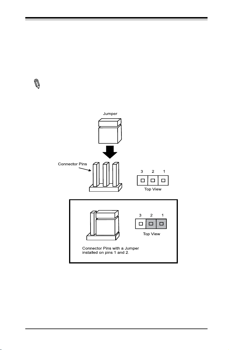
Chapter 2: Installation
2-6 Jumper Settings
Explanation of Jumpers
To modify the operation of the motherboard, jumpers can be used to choose between
optional settings. Jumpers create shorts between two pins to change the function
of the connector. Pin 1 is identied with a square solder pad on the printed circuit
board.
Note: On two pin jumpers, "Closed" means the jumper is on and "Open" means
the jumper is off the pins.
2-23
Page 62

X7SPA and X7SPE Motherboard Series User's Manual
MH2
MH3MH4
D17
JPW1
JUSB1
JD1
JPC3
JPUSB1
JWD1
JPG1
JBMC1
JPL1
JPT1
JPL2
JDIMM2
1
JDIMM1
JI2C2
JI2C1
JOH1
JL1
JL2
SP1
+
J2
J3
JBT1
JBAT1
JPCIE1
JUSB5
JUSB4
JUSB3
JUSB2
JLPC80
R1050
JSMB1
FAN1 FAN2
JCOM2
JCOM4
JPI2C1
JWF1
J8
JVGA1
CD1
JPB
FA N
FAN
COMS CLEAR
2-3 DISABLE
1-2 ENABLE
JPB:BMC ENABLE/DISABLE
CD-in
JPT1:TPM ENABLE/DISABLE
1-2 ENABLE
2-3 DISABLE
AUDIO FP
T-SGPIO2
T-SGPIO1
JPI2C:PWR I2C
JSMB1:SMBus1
JPUSB1:USB WAKE UP
2-3 DISABLE
1-2 ENABLE
JWF1:DOM PWR
JD1:1-3 PWR LED
4-7 SPEAKER
ON:ENABLEJI2C2
OFF:DISABLE
JI2C1
OFF:DISABLE
ON:ENABLE
JL2:AUDIO FRONT PANEL SELECT
ON:AC'97 FRONT PANEL
OFF:HD AUDIO FRONT PANEL
JPG1:VGA
2-3 DISABLE
1-2 ENABLE
2-3 DISABLE
JPL2:1-2 ENABLE
JPL1:1-2 ENABLE
2-3 DISABLE
JL1:CHASISS INTRUSION
JF1 PWR ON RST X OH/FF NIC2 NIC1 HDD LED PWR LED X NMI
2-3 NMI
JWD1:1-2 RST
JBT1:
LAN2
LAN1
I-SATA5
I-SATA2
I-SATA4
I-SATA1
I-SATA3
I-SATA0
SLOT1 PCI-E X4 (IN X16 SLOT)
SYS
CPU
KB/MOUSE
COM4
COM3
COM2
COM1
SODIMM2
SODIMM1
CPU
J6
J5
J10
J11
J12
J13
J14
JPF
LAN Port Enable/Disable
JPL1/JPL2 enable or disable LAN Port
1/LAN Port 2 on the motherboard. See
the table on the right for jumper set-
tings. The default setting is enabled.
Note: LAN Port 2 is not available
on the X7SPA-L.
SMB (I2C) Bus to PCI Slots
Jumpers JI2C1 and J I2C2 allow you to con-
nect the System Management Bus (SMB)
to PCI-E and PCI slots. The default setting
is set to Disabled. See the table on the
right for jumper settings.
GLAN Enable
Jumper Settings
Pin# Denition
1-2 Enabled (default)
2-3 Disabled
I2C to PCI-Slots
Jumper Settings
Jumper Denition
On Enabled
Off Disabled (Default)
LAN Port 1 Enable
A
B
LAN Port 2 Enable
(
X7SPA-H, X7SPA-HF, X7SPE-
HF, X7SPE-H, X7SPA-H-D525,
X7SPA-HF-D525, X7SPE-H-
D525, X7SPE-HF-D525 only)
2
JI
C1/JI2C2
C
2-24
A
B
C
Page 63

MH2
MH3MH4
D17
JPW1
JUSB1
JD1
JPC3
JPUSB1
JWD1
JPG1
JBMC1
JPL1
JPT1
JPL2
JDIMM2
1
JDIMM1
JI2C2
JI2C1
JOH1
JL1
JL2
SP1
+
J2
J3
JBT1
JBAT1
JPCIE1
JUSB5
JUSB4
JUSB3
JUSB2
JLPC80
R1050
JSMB1
FAN1 FAN2
JCOM2
JCOM4
JPI2C1
JWF1
J8
JVGA1
CD1
JPB
FA N
FAN
COMS CLEAR
2-3 DISABLE
1-2 ENABLE
JPB:BMC ENABLE/DISABLE
CD-in
JPT1:TPM ENABLE/DISABLE
1-2 ENABLE
2-3 DISABLE
AUDIO FP
T-SGPIO2
T-SGPIO1
JPI2C:PWR I2C
JSMB1:SMBus1
JPUSB1:USB WAKE UP
2-3 DISABLE
1-2 ENABLE
JWF1:DOM PWR
JD1:1-3 PWR LED
4-7 SPEAKER
ON:ENABLEJI2C2
OFF:DISABLE
JI2C1
OFF:DISABLE
ON:ENABLE
JL2:AUDIO FRONT PANEL SELECT
ON:AC'97 FRONT PANEL
OFF:HD AUDIO FRONT PANEL
JPG1:VGA
2-3 DISABLE
1-2 ENABLE
2-3 DISABLE
JPL2:1-2 ENABLE
JPL1:1-2 ENABLE
2-3 DISABLE
JL1:CHASISS INTRUSION
JF1 PWR ON RST X OH/FF NIC2 NIC1 HDD LED PWR LED X NMI
2-3 NMI
JWD1:1-2 RST
JBT1:
LAN2
LAN1
I-SATA5
I-SATA2
I-SATA4
I-SATA1
I-SATA3
I-SATA0
SLOT1 PCI-E X4 (IN X16 SLOT)
SYS
CPU
KB/MOUSE
COM4
COM3
COM2
COM1
SODIMM2
SODIMM1
CPU
J6
J5
J10
J11
J12
J13
J14
JPF
CMOS Clear
MH3MH4
JPW1
JD1
JPC3
JWD1
JDIMM2
1
JDIMM1
SP1
+
J2
J3
JBT1
JUSB5
JLPC80
R1050
JPI2C1
JWF1
COMS CLEAR
2-3 DISABLE
1-2 ENABLE
JPB:BMC ENABLE/DISABLE
JPT1:TPM ENABLE/DISABLE
1-2 ENABLE
2-3 DISABLE
T-SGPIO2
T-SGPIO1
JPI2C:PWR I2C
JPUSB1:USB WAKE UP
2-3 DISABLE
1-2 ENABLE
JWF1:DOM PWR
JD1:1-3 PWR LED
4-7 SPEAKER
ON:ENABLEJI2C2
OFF:DISABLE
JL2:AUDIO FRONT PANEL SELECT
ON:AC'97 FRONT PANEL
OFF:HD AUDIO FRONT PANEL
JPG1:VGA
2-3 DISABLE
1-2 ENABLE
2-3 DISABLE
JPL2:1-2 ENABLE
JPL1:1-2 ENABLE
2-3 DISABLE
JL1:CHASISS INTRUSION
JF1 PWR ON RST X OH/FF NIC2 NIC1 HDD LED PWR LED X NMI
2-3 NMI
JWD1:1-2 RST
JBT1:
I-SATA2
I-SATA1
I-SATA0
SODIMM2
SODIMM1
J14
JPF
JBT1 is used to clear CMOS. Instead
of pins, this "jumper" consists of contact
pads to prevent accidental clearing of
CMOS. To clear CMOS, use a metal
object such as a small screwdriver to
touch both pads at the same time to short
the connection. Always remove the AC
power cord from the system before clear-
ing CMOS.
Important: For an ATX power sup-
ply, you must completely shut down
the system, remove the AC power
cord and then short JBT1 to clear
CMOS.
Motherboard
A
Chapter 2: Installation
Metal contact pads
CMOS Clear
A
2-25
Page 64
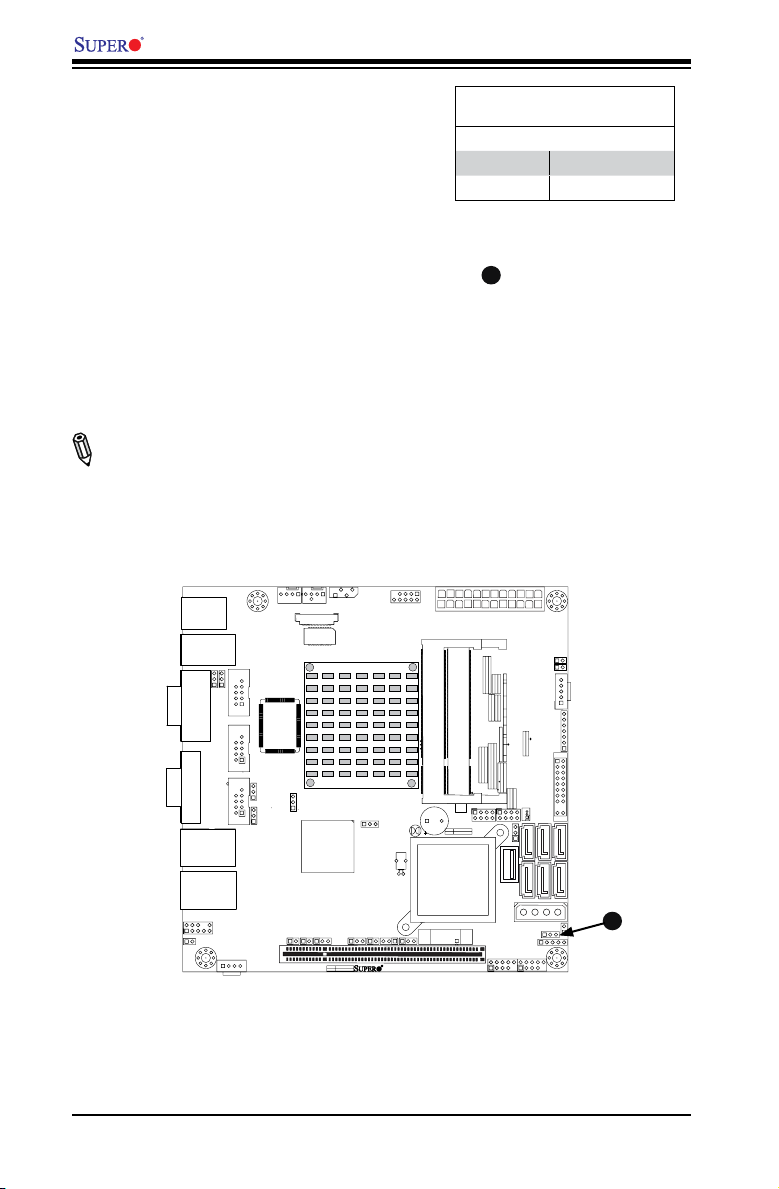
X7SPA and X7SPE Motherboard Series User's Manual
MH2
MH3MH4
D17
JPW1
JUSB1
JD1
JPC3
JPUSB1
JWD1
JPG1
JBMC1
JPL1
JPT1
JPL2
JDIMM2
1
JDIMM1
JI2C2
JI2C1
JOH1
JL1
JL2
SP1
+
J2
J3
JBT1
JBAT1
JPCIE1
JUSB5
JUSB4
JUSB3
JUSB2
JLPC80
R1050
JSMB1
FAN1 FAN2
JCOM2
JCOM4
JPI2C1
JWF1
J8
JVGA1
CD1
JPB
FA N
FAN
COMS CLEAR
2-3 DISABLE
1-2 ENABLE
JPB:BMC ENABLE/DISABLE
CD-in
JPT1:TPM ENABLE/DISABLE
1-2 ENABLE
2-3 DISABLE
AUDIO FP
T-SGPIO2
T-SGPIO1
JPI2C:PWR I2C
JSMB1:SMBus1
JPUSB1:USB WAKE UP
2-3 DISABLE
1-2 ENABLE
JWF1:DOM PWR
JD1:1-3 PWR LED
4-7 SPEAKER
ON:ENABLEJI2C2
OFF:DISABLE
JI2C1
OFF:DISABLE
ON:ENABLE
JL2:AUDIO FRONT PANEL SELECT
ON:AC'97 FRONT PANEL
OFF:HD AUDIO FRONT PANEL
JPG1:VGA
2-3 DISABLE
1-2 ENABLE
2-3 DISABLE
JPL2:1-2 ENABLE
JPL1:1-2 ENABLE
2-3 DISABLE
JL1:CHASISS INTRUSION
JF1 PWR ON RST X OH/FF NIC2 NIC1 HDD LED PWR LED X NMI
2-3 NMI
JWD1:1-2 RST
JBT1:
LAN2
LAN1
I-SATA5
I-SATA2
I-SATA4
I-SATA1
I-SATA3
I-SATA0
SLOT1 PCI-E X4 (IN X16 SLOT)
SYS
CPU
KB/MOUSE
COM4
COM3
COM2
COM1
SODIMM2
SODIMM1
CPU
J6
J5
J10
J11
J12
J13
J14
JPF
USB Wake-Up (Not Available on the
X7SPE-H-D525, X7SPA-H-D525, X7SPAHF-D525 and X7SPE-HF-D525)
Use JPUSB jumper to enable the function
of "System Waking-Up via USB devices".
This jumper allows you to "wake-up" the
system by pressing a key on the USB
keyboard or by clicking the USB mouse of
your system. The JPUSB jumper is used
together with the USB Wake-Up function in
the BIOS. Enable both the jumper and the
BIOS setting to activate this function. See
the table on the right for jumper settings
and jumper connections.
Note: The default jumper setting is "Dis-
abled". When the "USB Wake-Up" function
is enabled, it will be active on all USB
ports.
USB Wake-Up
Jumper Settings
Jumper Setting Denition
Pins 1-2 Enabled
Pins 2-3 Disabled (Default)
USB Wake-up
A
2-26
A
Page 65

TPM Support Enable (Not available
MH2
MH3MH4
D17
JPW1
JUSB1
JD1
JPC3
JPUSB1
JWD1
JPG1
JBMC1
JPL1
JPT1
JPL2
JDIMM2
1
JDIMM1
JI2C2
JI2C1
JOH1
JL1
JL2
SP1
+
J2
J3
JBT1
JBAT1
JPCIE1
JUSB5
JUSB4
JUSB3
JUSB2
JLPC80
R1050
JSMB1
FAN1 FAN2
JCOM2
JCOM4
JPI2C1
JWF1
J8
JVGA1
CD1
JPB
FA N
FAN
COMS CLEAR
2-3 DISABLE
1-2 ENABLE
JPB:BMC ENABLE/DISABLE
CD-in
JPT1:TPM ENABLE/DISABLE
1-2 ENABLE
2-3 DISABLE
AUDIO FP
T-SGPIO2
T-SGPIO1
JPI2C:PWR I2C
JSMB1:SMBus1
JPUSB1:USB WAKE UP
2-3 DISABLE
1-2 ENABLE
JWF1:DOM PWR
JD1:1-3 PWR LED
4-7 SPEAKER
ON:ENABLEJI2C2
OFF:DISABLE
JI2C1
OFF:DISABLE
ON:ENABLE
JL2:AUDIO FRONT PANEL SELECT
ON:AC'97 FRONT PANEL
OFF:HD AUDIO FRONT PANEL
JPG1:VGA
2-3 DISABLE
1-2 ENABLE
2-3 DISABLE
JPL2:1-2 ENABLE
JPL1:1-2 ENABLE
2-3 DISABLE
JL1:CHASISS INTRUSION
JF1 PWR ON RST X OH/FF NIC2 NIC1 HDD LED PWR LED X NMI
2-3 NMI
JWD1:1-2 RST
JBT1:
LAN2
LAN1
I-SATA5
I-SATA2
I-SATA4
I-SATA1
I-SATA3
I-SATA0
SLOT1 PCI-E X4 (IN X16 SLOT)
SYS
CPU
KB/MOUSE
COM4
COM3
COM2
COM1
SODIMM2
SODIMM1
CPU
J6
J5
J10
J11
J12
J13
J14
JPF
on X7SPA-H-D525, X7SPA-HF-D525,
X7SPE-H-D525, X7SPE-HF-D525)
JPT1 allows the user to enable TPM (Trust-
ed Platform Modules) support to enhance
data integrity and system security. See the
table on the right for jumper settings. The
default setting is enabled.
Chapter 2: Installation
TPM Support Enable
Jumper Settings
Jumper Setting Denition
1-2 Enabled
2-3 Disabled
(Default)
Watch Dog Enable/Disable
Watch Dog (JWD) is a system monitor that
can reboot the system when a software ap-
plication hangs. Close pins 1~2 to reset the
system if an application hangs. Close pins
2~3 to generate a non-maskable interrupt
Watch Dog
Jumper Settings (JWD)
Jumper Setting Denition
Pins 1-2 Reset
(default)
Pins 2-3 NMI
Open Disabled
signal for the application that hangs. See
the table on the right for jumper settings.
COM3 Select (JPC3)
Watch Dog must also be enabled in the
BIOS.
COM3 Redirection Select (OEM
Option)
This is an OEM option for the X7SPA-H,
Jumper Setting Denition
Pins 1-2 RS232
(default)
Pins 2-3 TTL
Open Disabled
X7SPA-HF, X7SPE-H, X7SPE-HF, X7SPE-
H-D525, X7SPA-H-D525, X7SPA-HF-D525
and X7SPE-HF-D525 only.
TPM Enable
A
Watch Dog Enable
B
COM3 Redirect
C
(OEM option for the
X7SPA-H, X7SPA-HF,
X7SPE-H, X7SPEHF, X7SPA-H-D525,
X 7 S PA - H F- D5 25 ,
X7SPE-H-D525, and
X 7 S P E- H F -D 5 25
only).
B
2-27
A
C
Page 66

X7SPA and X7SPE Motherboard Series User's Manual
MH2
MH3MH4
D17
JPW1
JUSB1
JD1
JPC3
JPUSB1
JWD1
JPG1
JBMC1
JPL1
JPT1
JPL2
JDIMM2
1
JDIMM1
JI2C2
JI2C1
JOH1
JL1
JL2
SP1
+
J2
J3
JBT1
JBAT1
JPCIE1
JUSB5
JUSB4
JUSB3
JUSB2
JLPC80
R1050
JSMB1
FAN1 FAN2
JCOM2
JCOM4
JPI2C1
JWF1
J8
JVGA1
CD1
JPB
FA N
FAN
COMS CLEAR
2-3 DISABLE
1-2 ENABLE
JPB:BMC ENABLE/DISABLE
CD-in
JPT1:TPM ENABLE/DISABLE
1-2 ENABLE
2-3 DISABLE
AUDIO FP
T-SGPIO2
T-SGPIO1
JPI2C:PWR I2C
JSMB1:SMBus1
JPUSB1:USB WAKE UP
2-3 DISABLE
1-2 ENABLE
JWF1:DOM PWR
JD1:1-3 PWR LED
4-7 SPEAKER
ON:ENABLEJI2C2
OFF:DISABLE
JI2C1
OFF:DISABLE
ON:ENABLE
JL2:AUDIO FRONT PANEL SELECT
ON:AC'97 FRONT PANEL
OFF:HD AUDIO FRONT PANEL
JPG1:VGA
2-3 DISABLE
1-2 ENABLE
2-3 DISABLE
JPL2:1-2 ENABLE
JPL1:1-2 ENABLE
2-3 DISABLE
JL1:CHASISS INTRUSION
JF1 PWR ON RST X OH/FF NIC2 NIC1 HDD LED PWR LED X NMI
2-3 NMI
JWD1:1-2 RST
JBT1:
LAN2
LAN1
I-SATA5
I-SATA2
I-SATA4
I-SATA1
I-SATA3
I-SATA0
SLOT1 PCI-E X4 (IN X16 SLOT)
SYS
CPU
KB/MOUSE
COM4
COM3
COM2
COM1
SODIMM2
SODIMM1
CPU
J6
J5
J10
J11
J12
J13
J14
JPF
Power LED/Speaker
On the JD1 header, pins 1~3 are used
for a power LED and pins 4~7 are
used for an external speaker. If you
wish to use the onboard speaker, you
should close pins 6-7 with a jumper.
Speaker Connector
Pin Setting Denition
Pins 6-7 Internal Speaker
Pins 4-7 External Speaker
See the table on the right for speaker
pin denitions.
PinDenitions
BMC (X7SPA-HF, X7SPE-HF,
X7SPE-HF-D525, X7SPA-H-D525,
X7SPA-HF-D525 Only)
The JPB jumper is used to enable or
disable the on-board Baseboard Man-
Pin Setting Denition
Pins 1-2 Enabled (Default)
Pins 2-3 Disabled
BMC
PinDenitions
agement Controller (BMC) and the
Power LED/Speaker
on-board IPMI feature. This jumper is
used together with the IPMI settings in
A
BMC Enable
B
the BIOS. The default position is pins
1 and 2 to enable BMC. See the table
on the right for jumper settings.
A
B
2-28
Page 67

Chapter 2: Installation
MH2
MH3MH4
D17
JPW1
JUSB1
JD1
JPC3
JPUSB1
JWD1
JPG1
JBMC1
JPL1
JPT1
JPL2
JDIMM2
1
JDIMM1
JI2C2
JI2C1
JOH1
JL1
JL2
SP1
+
J2
J3
JBT1
JBAT1
JPCIE1
JUSB5
JUSB4
JUSB3
JUSB2
JLPC80
R1050
JSMB1
FAN1 FAN2
JCOM2
JCOM4
JPI2C1
JWF1
J8
JVGA1
CD1
JPB
FA N
FAN
COMS CLEAR
2-3 DISABLE
1-2 ENABLE
JPB:BMC ENABLE/DISABLE
CD-in
JPT1:TPM ENABLE/DISABLE
1-2 ENABLE
2-3 DISABLE
AUDIO FP
T-SGPIO2
T-SGPIO1
JPI2C:PWR I2C
JSMB1:SMBus1
JPUSB1:USB WAKE UP
2-3 DISABLE
1-2 ENABLE
JWF1:DOM PWR
JD1:1-3 PWR LED
4-7 SPEAKER
ON:ENABLEJI2C2
OFF:DISABLE
JI2C1
OFF:DISABLE
ON:ENABLE
JL2:AUDIO FRONT PANEL SELECT
ON:AC'97 FRONT PANEL
OFF:HD AUDIO FRONT PANEL
JPG1:VGA
2-3 DISABLE
1-2 ENABLE
2-3 DISABLE
JPL2:1-2 ENABLE
JPL1:1-2 ENABLE
2-3 DISABLE
JL1:CHASISS INTRUSION
JF1 PWR ON RST X OH/FF NIC2 NIC1 HDD LED PWR LED X NMI
2-3 NMI
JWD1:1-2 RST
JBT1:
LAN2
LAN1
I-SATA5
I-SATA2
I-SATA4
I-SATA1
I-SATA3
I-SATA0
SLOT1 PCI-E X4 (IN X16 SLOT)
SYS
CPU
KB/MOUSE
COM4
COM3
COM2
COM1
SODIMM2
SODIMM1
CPU
J6
J5
J10
J11
J12
J13
J14
JPF
VGA Enable (X7SPA-HF, X7SPE-HF,
X7SPE-HF-D525, X7SPA-HF-D525 only)
JPG1 allows the user to enable or disable
the onboard VGA adapter on the X7SPA-HF,
X7SPE-HF, X7SPA-HF-D525 and X7SPE-
HF-D525. The default setting is Enabled.
HDA/AC97 Select (X7SPA-L Only)
JL2 allows the user to select between High
Denition Audio (HDA) or legacy AC97 audio.
The default setting is HD Audio.
VGA Enable
Jumper Settings
Pin# Denition
1-2 Enabled (default)
2-3 Disabled
HDA/AC97
Jumper Settings
Pin# 1-2 Denition
Open HD Audio (default)
Closed AC97
VGA Enable
A
HDA/AC97 Select
B
A
B
2-29
Page 68

X7SPA and X7SPE Motherboard Series User's Manual
MH2
MH3MH4
D17
JPW1
JUSB1
JD1
JPC3
JPUSB1
JWD1
JPG1
JBMC1
JPL1
JPT1
JPL2
JDIMM2
1
JDIMM1
JI2C2
JI2C1
JOH1
JL1
JL2
SP1
+
J2
J3
JBT1
JBAT1
JPCIE1
JUSB5
JUSB4
JUSB3
JUSB2
JLPC80
R1050
JSMB1
FAN1 FAN2
JCOM2
JCOM4
JPI2C1
JWF1
J8
JVGA1
CD1
JPB
FA N
FAN
COMS CLEAR
2-3 DISABLE
1-2 ENABLE
JPB:BMC ENABLE/DISABLE
CD-in
JPT1:TPM ENABLE/DISABLE
1-2 ENABLE
2-3 DISABLE
AUDIO FP
T-SGPIO2
T-SGPIO1
JPI2C:PWR I2C
JSMB1:SMBus1
JPUSB1:USB WAKE UP
2-3 DISABLE
1-2 ENABLE
JWF1:DOM PWR
JD1:1-3 PWR LED
4-7 SPEAKER
ON:ENABLEJI2C2
OFF:DISABLE
JI2C1
OFF:DISABLE
ON:ENABLE
JL2:AUDIO FRONT PANEL SELECT
ON:AC'97 FRONT PANEL
OFF:HD AUDIO FRONT PANEL
JPG1:VGA
2-3 DISABLE
1-2 ENABLE
2-3 DISABLE
JPL2:1-2 ENABLE
JPL1:1-2 ENABLE
2-3 DISABLE
JL1:CHASISS INTRUSION
JF1 PWR ON RST X OH/FF NIC2 NIC1 HDD LED PWR LED X NMI
2-3 NMI
JWD1:1-2 RST
JBT1:
LAN2
LAN1
I-SATA5
I-SATA2
I-SATA4
I-SATA1
I-SATA3
I-SATA0
SLOT1 PCI-E X4 (IN X16 SLOT)
SYS
CPU
KB/MOUSE
COM4
COM3
COM2
COM1
SODIMM2
SODIMM1
CPU
J6
J5
J10
J11
J12
J13
J14
JPF
Power Force On Enable/Disable
Jumper JPF allows you to enable (force on) or
disable the Power Force On function. If enabled,
the power will always stay on automatically. If
this function is disabled (the normal setting), the
Power Force On
Enable/Disable
Jumper Settings
Jumper Setting Denition
Open Normal
Closed Force On
user needs to press the power button to power
on the system.
DCD / P5V Select
This is an OEM option for the X7SPA-H, X7SPA-
HF, X7SPE-H, X7SPE-HF, X7SPE-H-D5 25 ,
X7SPE-HF-D525, X7SPA-H-D525, and X7SPA-
HF-D525 only.
A
B
C
D
E
DCD / P5V Select
Jumper Settings
Jumper Setting Denition
Pins 1-2 DCD
Pins 2-3 P5V
Power Force On
DCD / P5V Select (COM1)
DCD / P5V Select (COM2)
DCD / P5V Select (COM3)
DCD / P5V Select (COM4)
C
B
E
D
A
2-30
Page 69

Chapter 2: Installation
MH2
MH3MH4
D17
JPW1
JUSB1
JD1
JPC3
JPUSB1
JWD1
JPG1
JBMC1
JPL1
JPT1
JPL2
JDIMM2
1
JDIMM1
JI2C2
JI2C1
JOH1
JL1
JL2
SP1
+
J2
J3
JBT1
JBAT1
JPCIE1
JUSB5
JUSB4
JUSB3
JUSB2
JLPC80
R1050
JSMB1
FAN1 FAN2
JCOM2
JCOM4
JPI2C1
JWF1
J8
JVGA1
CD1
JPB
FA N
FAN
COMS CLEAR
2-3 DISABLE
1-2 ENABLE
JPB:BMC ENABLE/DISABLE
CD-in
JPT1:TPM ENABLE/DISABLE
1-2 ENABLE
2-3 DISABLE
AUDIO FP
T-SGPIO2
T-SGPIO1
JPI2C:PWR I2C
JSMB1:SMBus1
JPUSB1:USB WAKE UP
2-3 DISABLE
1-2 ENABLE
JWF1:DOM PWR
JD1:1-3 PWR LED
4-7 SPEAKER
ON:ENABLEJI2C2
OFF:DISABLE
JI2C1
OFF:DISABLE
ON:ENABLE
JL2:AUDIO FRONT PANEL SELECT
ON:AC'97 FRONT PANEL
OFF:HD AUDIO FRONT PANEL
JPG1:VGA
2-3 DISABLE
1-2 ENABLE
2-3 DISABLE
JPL2:1-2 ENABLE
JPL1:1-2 ENABLE
2-3 DISABLE
JL1:CHASISS INTRUSION
JF1 PWR ON RST X OH/FF NIC2 NIC1 HDD LED PWR LED X NMI
2-3 NMI
JWD1:1-2 RST
JBT1:
LAN2
LAN1
I-SATA5
I-SATA2
I-SATA4
I-SATA1
I-SATA3
I-SATA0
SLOT1 PCI-E X4 (IN X16 SLOT)
SYS
CPU
KB/MOUSE
COM4
COM3
COM2
COM1
SODIMM2
SODIMM1
CPU
J6
J5
J10
J11
J12
J13
J14
JPF
2-7 Onboard Indicators
LAN Port LEDs
Two LAN ports are loc ated on the I/O
Backplane. Each Ethernet LAN port has
two LEDs. The yellow Activity LED (right,
see below) indicates activity, while the Link/
Speed LED (left) may be green, amber or off
to indicate the speed of the connection. See
the tables at right for more information.
Link/Speed LED
Rear View (when facing the
rear side of the chassis)
Activity LED
GLAN Link/Speed LED Indicator
LED Color Denition
Off No Connection or 10 Mbps
Green (On) 100 Mbps
Amber (On) 1 Gbps
GLAN Activity LED Indicator
Color Denition
Yellow (Flashing) ConnectionActive
A
LAN Port 1
B
LAN Port 2 (Not available on
the X7SPA-L)
A
B
2-31
Back Panel Connectors
Page 70

X7SPA and X7SPE Motherboard Series User's Manual
MH2
MH3MH4
D17
JPW1
JUSB1
JD1
JPC3
JPUSB1
JWD1
JPG1
JBMC1
JPL1
JPT1
JPL2
JDIMM2
1
JDIMM1
JI2C2
JI2C1
JOH1
JL1
JL2
SP1
+
J2
J3
JBT1
JBAT1
JPCIE1
JUSB5
JUSB4
JUSB3
JUSB2
JLPC80
R1050
JSMB1
FAN1 FAN2
JCOM2
JCOM4
JPI2C1
JWF1
J8
JVGA1
CD1
JPB
FA N
FAN
COMS CLEAR
2-3 DISABLE
1-2 ENABLE
JPB:BMC ENABLE/DISABLE
CD-in
JPT1:TPM ENABLE/DISABLE
1-2 ENABLE
2-3 DISABLE
AUDIO FP
T-SGPIO2
T-SGPIO1
JPI2C:PWR I2C
JSMB1:SMBus1
JPUSB1:USB WAKE UP
2-3 DISABLE
1-2 ENABLE
JWF1:DOM PWR
JD1:1-3 PWR LED
4-7 SPEAKER
ON:ENABLEJI2C2
OFF:DISABLE
JI2C1
OFF:DISABLE
ON:ENABLE
JL2:AUDIO FRONT PANEL SELECT
ON:AC'97 FRONT PANEL
OFF:HD AUDIO FRONT PANEL
JPG1:VGA
2-3 DISABLE
1-2 ENABLE
2-3 DISABLE
JPL2:1-2 ENABLE
JPL1:1-2 ENABLE
2-3 DISABLE
JL1:CHASISS INTRUSION
JF1 PWR ON RST X OH/FF NIC2 NIC1 HDD LED PWR LED X NMI
2-3 NMI
JWD1:1-2 RST
JBT1:
LAN2
LAN1
I-SATA5
I-SATA2
I-SATA4
I-SATA1
I-SATA3
I-SATA0
SLOT1 PCI-E X4 (IN X16 SLOT)
SYS
CPU
KB/MOUSE
COM4
COM3
COM2
COM1
SODIMM2
SODIMM1
CPU
J6
J5
J10
J11
J12
J13
J14
JPF
2-8 Serial ATA and HDD Connections
Note the following conditions when connecting the Serial ATA and hard disk drive
cables:
• Be sure to use the correct cable for each connector. Refer to Page 1-1 for cables
that came with your shipment.
SATA Connectors
Six (6) Serial ATA (SATA) connectors
(I-SATA 0~5) are located on the mother-
board, to provide serial link connections.
Serial Link connections provide faster
data transmission than those of the tra-
ditional Parallel ATA. These four SATA
connectors are supported by the Intel
ICH9/9R South Bridge. See the table on
SATA Connectors
PinDenitions
Pin# Signal
1 Ground
2 SATA_TXP
3 SATA_TXN
4 Ground
5 SATA_RXN
6 SATA_RXP
7 Ground
the right for pin denitions.
Note: There are Four (4) SATA ports on
the X7SPA-L.
2-32
I-SATA0
A
I-SATA1
B
I-SATA2*
C
I-SATA3*
D
I-SATA4
E
I-SATA5
F
*I-SATA2 and I-SATA3 are not
available on the X7SPA-L.
C
B
A
F
E
D
Page 71

Chapter 3: Troubleshooting
Chapter 3
Troubleshooting
3-1 Troubleshooting Procedures
Use the following procedures to troubleshoot your system. If you have followed all
of the procedures below and still need assistance, refer to the ‘Technical Support
Procedures’ and/or ‘Returning Merchandise for Service’ section(s) in this chapter.
Always disconnect the AC power cord before adding, changing or installing any
hardware components.
Before Power On
1. Be sure to unplug the power cable before installing or removing the compo-
nents.)
2. Make sure that there are no short circuits between the motherboard and chas-
sis.
3. Disconnect all ribbon/wire cables from the motherboard, including those for the
keyboard and mouse. Also, be sure to remove all add-on cards.
4. Connect the chassis speaker and the power LED to the motherboard. Check
all jumper settings as well.
No Power
1. Make sure that there are no short circuits between the motherboard and chas-
sis.
2. Make sure that all jumpers are set to their default positions.
3. Check if the 115V/230V switch on the power supply is properly set.
4. Turn the power switch on and off to test the system.
5. The battery on your motherboard may be old. Check to make sure that it still
supplies ~3VDC. If it does not, replace it with a new one.
No Video
1. If the power is on, but you have no video--in this case, you will need to remove
all the add-on cards and cables rst.
3-1
Page 72

X7SPA and X7SPE Motherboard Series User's Manual
2. Use the speaker to determine if any beep codes exist. (Refer to Appendix A
for details on beep codes.)
3. Remove all memory modules and turn on the system. (If the alarm is on, check
the specs of memory modules, reset the memory or try a dif ferent one.)
Memory Errors
1. Make sure that the SO- DIMM modules are properly installed and fully seated
in the slots.
2. Please ch eck Se ction 2- 3 a nd ma ke sure th at yo u a re us ing the c orrec t m emory.
Also, it is recommended that you use the memory modules of the same type
and speed for all DIMMs in the system.
3. Check for bad DIMM modules or slots by swapping modules between slots to
see if you can locate the faulty modules.
4. Check the power supply voltage 115V/230V switch.
LosingtheSystem’sSetupConguration
1. Please be sure to use a high quality power supply. A poor quality power supply
may cause the system to lose the CMOS setup information. Refer to Section
1-5 for details on recommended power supplies.
2. The batter y on your motherboard may be old. Check to verify that it still supplies
~3VDC. If it does not, replace it with a new one.
3. If the above steps do not x the Setup Conguration problem, contact your
vendor for repairs.
3-2 Technical Support Procedures
Before contacting Technical Support, please make sure that you have followed all
the steps listed below. Also, Note that as a motherboard manufacturer, Supermicro
does not sell directly to end users, so it is best to rst check with your distributor or
reseller for troubleshooting services. They should know of any possible problem(s)
with the specic system conguration that was sold to you.
1. Please go through the ‘Troubleshooting Procedures’ and 'Frequently Asked
Question' (FAQ) sections in this chapter or see the FAQs on our website
(http://www.supermicro.com/support/faqs/) befo re contacting Technica l
Suppor t.
2. BIOS upgrades can be downloaded from our website at (http://www.supermicro.
com/support/bios/).
3-2
Page 73

Chapter 3: Troubleshooting
Note: Not all BIOS can be ashed. Some cannot be ashed; it depends
on the modications to the boot block code.
3. If you've followed the instructions above to troubleshoot your system, and
still cannot resolve the problem, then contact Supermicro's technical support and
provide them with the following information:
Motherboard model and PCB revision number•
BIOS release date/version (this can be seen on the initial display when your •
system rst boots up)
System conguration (OS version, peripheral devices, power supply type, etc)•
An example of a Technical Suppor t form is on our website at (http://www.
supermicro.com/support/contact.cfm).
4. Distributors: For immediate assistance, please have your account number ready
when placing a call to our technical support department. We can be reached
by e-mail at support@supermicro.com, by phone at: (408) 503-8000, option
2, or by fax at (408)503-8019.
3-3 Frequently Asked Questions
Question: What type of memory does my motherboard support?
Answer:
The X7SPA-L, X7SPA-H, X7SPA-HF, X7SPE- H, X7SPE-HF supports up to
4GB of unbuffered Non-ECC DDR2 667/800 MHz, two-way interleaved or
non-interleaved SO DIMM SDRAM. See Section 2-4 for details on installing
memory.
The X7SPE-H-D525, X7SPA-HF-D525, X7SPA-H-D525 and X7SPE-HF-D525
supports up to 4GB of unbuffered Non-ECC DDR3 800MHz, two-way inter-
leaved or non-interleaved SO DIMM SDRAM
Question: Why does Microsoft Windows XP (SP2) and Windows Vista show
less memory than what is physically installed?
Answer: Microsoft implemented a design change in Windows XP with Service
Pack 2 (SP2) and Windows Vista. This change is specic to the Physical Ad-
dress Extension (PAE) mode behavior which improves driver compatibility. For
more information, please read the following article at Microsoft’s Knowledge
Base website at: http://support.microsoft.com/kb/888137.
3-3
Page 74

X7SPA and X7SPE Motherboard Series User's Manual
Question: How do I update my BIOS?
Answer: It is recommended that you do not upgrade your BIOS if you are not
experiencing any problems with your system. Updated BIOS les are located
on our web site at http://www.supermicro.com/support/bios/. Please check our
BIOS warning message and the information on how to update your BIOS on our
web site. Select your motherboard model and download the BIOS (.rom) le to
your computer. Also, check the current BIOS revision and make sure that it is
newer than your BIOS before downloading. You may choose the zip le or the
.exe le. If you choose the zipped BIOS le, please unzip the BIOS le onto a
bootable device or a USB pen/thumb drive. To ash the BIOS, run the batch
le named "ami.bat" with the new BIOS ROM le from your bootable device or
USB pen/thumb drive. Use the following format:
F:\> ami.bat BIOS-ROM-lename.x xx <Enter>
Notes: Always use the le named “ami.bat” to update the BIOS and insert a
space between "ami.bat" and the lename. The BIOS -ROM-lename will bear
the motherboard name (i.e., X7SPA) and build version as the extension. For
exa mp le, "X7SPA0.526".
When completed, your system will automatically reboot. If you choose the .exe
le, please run the .exe le under Windows to create the BIOS ash oppy disk.
Insert the oppy disk into the system you wish to ash the BIOS. Then, boot
the system to the oppy disk. The BIOS utility will automatically ash the BIOS
without any prompts. Please note that this process may take a few minutes to
complete. Do not be concerned if the screen is paused for a few minutes.
Warning: Do not shut down or reset the system while updating the BIOS
to prevent possible system boot failure!
When the BIOS ashing screen is completed, the system will reboot and will
show “Press F1 or F2”. At this point, you will need to load the BIOS defaults.
Press <F1> to go to the BIOS setup screen, and press <F9> to load the default
settings. Next, press <F10> to save and exit. The system will then reboot.
Note: The SPI BIOS chip installed on this motherboard is not removable. To
repair or replace a damaged BIOS chip, please send your motherboard to RMA
at Supermicro for service.
Question: What's on the CD that came with my motherboard?
Answer: The supplied compact disc has quite a few drivers and programs
that will greatly enhance your system. We recommend that you review the CD
and install the applications you need. Applications on the CD include chipset
drivers for Windows, security and audio drivers.
3-4
Page 75

Chapter 3: Troubleshooting
3-4 Returning Merchandise for Service
A receipt or copy of your invoice marked with the date of purchase is required
before any warranty ser vice will be rendered. You can obtain service by calling
your vendor for a Returned Merchandise Authorization (RMA) number. When
returning to the manufacturer, the RMA number should be prominently displayed
on the outside of the shipping carton, and mailed prepaid or hand-carried. Ship-
ping and handling charges will be applied for all orders that must be mailed when
service is complete.
This warranty only covers normal consumer use and does not cover damages
incurred in shipping or from failure due to the alteration, misuse, abuse or improper
maintenance of products.
During the warranty period, contact your distributor rst for any product prob-
lems.
3-5
Page 76

X7SPA and X7SPE Motherboard Series User's Manual
Notes
3-6
Page 77

Chapter 4: AMI BIOS
Chapter 4
BIOS
4-1 Introduction
This chapter describes the AMI BIOS Setup Utility for the X7SPA and X7SPE series.
The AMI ROM BIOS is stored in a Flash EEPROM and can be easily updated.
This chapter describes the basic navigation of the AMI BIOS Setup Utility setup
screens.
Note: For instructions on BIOS recovery, please refer to the instruction
guide posted at http://www.supermicro.com/support/manuals/.
Starting BIOS Setup Utility
To enter the AMI BIOS Setup Utility screens, press the <Delete> key while the
system is booting up.
Note: In most cases, the <Delete> key is used to invoke the AMI BIOS
setup screen. There are a few cases when other keys are used, such as
<F1>, <F2>, etc.
Each main BIOS menu option is described in this manual. The Main BIOS setup
menu screen has two main frames. The left frame displays all the options that can
be congured. Grayed-out options cannot be congured. Options in blue can be
congured by the user. The right frame displays the key legend. Above the key
legend is an area reserved for a text message. When an option is selected in the
left frame, it is highlighted in white. Often a text message will accompany it. (Note:
the AMI BIOS has default text messages built in. Supermicro retains the option to
include, omit, or change any of these text messages.)
The AMI BIOS Setup Utility uses a key-based navigation system called "hot keys".
Most of the AMI BIOS setup utility "hot keys" can be used at any time during the
setup navigation process. These keys include <F1>, <F10>, <Enter>, <ESC>, ar-
row keys, etc.
Note: Options printed in Bold are default settings.
HowToChangetheCongurationData
The conguration data that determines the system parameters may be changed by
entering the AMI BIOS Setup utility. This Setup utility can be accessed by pressing
<Del> at the appropriate time during system boot.
4-1
Page 78

X7SPA and X7SPE Motherboard Series User's Manual
How to Start the Setup Utility
Normally, the only visible Power-On Self-Test (POST) routine is the memory test.
As the memory is being tested, press the <Delete> key to enter the main menu of
the AMI BIOS Setup Utility. From the main menu, you can access the other setup
screens. An AMI BIOS identication string is displayed at the left bottom corner of
the screen, below the copyright message.
Warning! Do not upgrade the BIOS unless your system has a BIOS-related
issue. Flashing the wrong BIOS can cause irreparable damage to the
system. In no event shall Supermicro be liable for direct, indirect, special,
incidental, or consequential damages arising from a BIOS update. If you
have to update the BIOS, do not shut down or reset the system while the
BIOS is updating. This is to avoid possible boot failure.
4-2 Main Setup
When you rst enter the AMI BIOS Setup Utility, you will enter the Main setup screen.
You can always return to the Main setup screen by selecting the Main tab on the
top of the screen. The Main BIOS Setup screen is shown below.
4-2
Page 79

Chapter 4: AMI BIOS
System Overview: The following BIOS information will be displayed:
System Time/System Date
Use this option to change the system time and date. Highlight System Time or Sys-
tem Date using the arrow keys. Enter new values through the keyboard. Press the
<Tab> key or the arrow keys to move between elds. The date must be entered in
Day MM/DD/YY format. The time is entered in HH:MM:SS format. (Note: The time
is in the 24-hour format. For example, 5:30 P.M. appears as 17:30:00.)
Supermicro X7SPA-L/X7SPA-H/X7SPA-HF/X7SPE-H/X7SPE-HF/X7SPE-H-D525/
X7SPE-HF-D525/X7SPA-H-D525/X7SPA-HF-D525
Version
Build Date
Processor
The AMI BIOS will automatically display the status of processor as shown below:
Type of Processor
Speed
Physical Count
Logical Count
System Memory
This displays the size of memory available in the system:
Populated Size
Available Size
4-3
Page 80

X7SPA and X7SPE Motherboard Series User's Manual
4-3 AdvancedSetupCongurations
Use the arrow keys to select Boot Setup and hit <Enter> to access the submenu
items:
BOOT Feature
Quick Boot
If Enabled, this option will skip certain tests during POST to reduce the time needed
for system boot. The options are Enabled and Disabled.
Quiet Boot
This option allows the bootup screen options to be modied between POST mes-
sages or the OEM logo. Select Disabled to display the POST messages. Select
Enabled to display the OEM logo instead of the normal POST messages. The op-
tions are Enabled and Disabled.
AddOn ROM Display Mode
This sets the display mode for Option ROM. The options are Force BIOS and
Keep Current.
4-4
Page 81

Chapter 4: AMI BIOS
Bootup Num-Lock
This feature selects the Power-on state for Numlock key. The options are Of f
and On.
PS/2 Mouse Support
This feature enables support for the PS/2 mouse. The options are Disabled,
Enabled and Auto.
Wait For 'F1' If Error
This forces the system to wait until the 'F1' key is pressed if an error occurs. The
options are Disabled and Enabled.
Hit 'Del' Message Display
This feature displays "Press DEL to run Setup" during POST. The options are
Enabled and Disabled.
Watch Dog Function
If enabled, the Watch Dog Timer will allow the system to reboot when it is inactive
for more than 5 minutes. The options are Enabled and Disabled.
Power Button Function
This setting allows you to decide if the power button will turn off the system in-
stantly or wait for 4 seconds when it is pressed. The options are Instant Off and
4 Seconds Override.
Restore on AC Power Loss
Use this feature to set the power state after a power outage. Select Power-Off for
the system power to remain off after a power loss. Select Power-On for the system
power to be turned on after a power loss. Select Last State to allow the system to
resume its last state before a power loss. The options are Power-On, Power-Off
and Last State.
Interrupt 19 Capture
Interrupt 19 is the software interrupt that handles the boot disk function. When this
item is set to Enabled, the ROM BIOS of the host adaptors will "capture" Interrupt
19 at boot and allow the drives that are attached to these host adaptors to function
as bootable disks. If this item is set to Disabled, the ROM BIOS of the host adap-
tors will not capture Interrupt 19, and the drives attached to these adaptors will not
function as bootable devices. The options are Enabled and Disabled.
4-5
Page 82

X7SPA and X7SPE Motherboard Series User's Manual
Standby Power in S5
This feature supplies standby power while in S5 (sleep mode). Set this feature to
Disabled to comply with EuP requirements, Enable this feature to activate wake-up
capability while in sleep mode. The options are Enabled and Disabled.
CPUConguration
Warning: Take Caution when changing the Advanced settings. An incorrect
value, a very high DRAM frequency or incorrect DRAM timing may cause
system to become unstable. When this occurs, revert to the default setting.
Clock Spread Spectrum
Select Enable to use the feature of Clock Spectrum, which will allow the BIOS to
monitor and attempt to reduce the level of Electromagnetic Interference caused by
the components whenever needed. Select Disabled to enhance system stability.
The options are Disabled and Enabled.
Max CPUID Value Limit
This feature allows the user to set the maximum CPU ID value. Enable this function
to boot the legacy operating systems that cannot support processors with extended
CPUID functions. The options are Enabled and Disabled (for the Windows OS.).
Execute-Disable Bit Capability (Available when supported by the OS and
the CPU)
Set to Enabled to enable the Execute Disable Bit which will allow the processor
to designate areas in the system memory where an application code can execute
and where it cannot, thus preventing a worm or a virus from ooding illegal codes
to overwhelm the processor or damage the system during an attack. The default is
Enabled. (Refer to Intel and Microsoft Web Sites for more information.)
Hyper-threading Technology
This setting allows you to Enab le o r Di sab le h ype r- thr ead ing in t he C PU. En abl ing
hyper-threading results in increased CPU per formance.
4-6
Page 83

Chapter 4: AMI BIOS
Advanced Chipset Control
The items included in the Advanced Settings submenu are listed below.
NorthbridgeConguration
DRAM Frequency
This option allows the user to select the desired frequency setting for the onboard
memory modules. The options are Auto, 667 MHz and 800 MHz. (667 MHz is
not available on the X7SPE-H-D525, X7SPA-HF-D525 and X7SPE-HF-D525).
CongureDRAMTimingbySPD
This option allows the user to select the desired DRAM timing for the onboard
memory modules. The options are Enabled and Disabled. The following will
appear when Disabled is selected:
DRAM CAS# Latency
The options are [3], [4], [5], and [6]
DRAM RAS# to CAS# Delay
The options are 3 DRAM Clocks, 4 DRAM Clocks, 5 DRAM Clocks, and
6 DRAM Clocks.
DRAM RAS# Precharge
The options are 3 DRAM Clocks, 4 DRAM Clocks, 5 DRAM Clocks, and
6 DRAM Clocks.
DRAM RAS# Activate to Precharge
The options are 9 DRAM Clocks, 10 DRAM Clocks, 11 DRAM Clocks,
12 DRAM Clocks, 13 DRAM Clocks, 14 DRAM Clocks, and 15 DRAM
Clocks.
Initiate Graphics Adapter
This option selects which graphics adapter to use as a primary boot device. The
options are Other, Onboard VGA and Slot6.
Internal Graphics Mode Select
This option selects the amount of system memory used by the onboard graphics
adapter. The options are Enabled, 8MB.
4-7
Page 84

X7SPA and X7SPE Motherboard Series User's Manual
VideoFunctionConguration(X7SPA-L,X7SPE-H,
X7SPA-H-D525 and X7SPE-H-D525 only)
DVMT Mode Select
Select DVMT Mode to enable Dynamic Video Memory Technology (DVMT).
The options are Fixed Mode and DVMT Mode.
DVMT/Fixed Memory
This item selects the DVMT/Fixed memory size. The options are 128MB,
256MB and Maximum DVMT.
Boot Display Device
This item selects the display device the motherboard uses during system
boot. The options are CRT, LVDS and CRT + LVDS.
Alternate Video BIOS
This item selects the display BIOS used by the motherboard. The options
are Auto, Standard and Customize.
Active State Power Management
Select Enabled to start Active-State Power Management for signal transactions
between L0 and L1 Links on the PCI Express Bus. This maximizes power-saving
and transaction speed. The options are Enabled and Disabled.
Reserved Page Route
This feature allows the user to decide which bus to send debug information to. The
options are Disabled, PCI and LPC.
USB Functions
This feature allows the user to decide the number of onboard USB ports to be en-
abled. The Options are: Disabled, 2 USB ports, 4 USB ports, 6 USB ports, 8 USB
ports, 10 USB ports, and 12 USB ports.
Legacy USB Support (available if USB Functions above is Enabled)
Select Enabled to use Legacy USB devices. If this item is set to Auto, Legacy
USB support will be automatically enabled if a legacy USB device is installed
4-8
Page 85

Chapter 4: AMI BIOS
on the motherboard, and vise versa. The settings are Disabled, Enabled
and Auto.
USB Controller
This feature allows the user to Enable or Disable the onboard USB controller. The
options are Enabled and Disabled. Note: This function is grayed-out if USB Func-
tions above is set to Enabled.
IDE/SATAConguration
When this submenu is selected, the AMI BIOS automatically detects the presence
of the IDE Devices and displays the following items:
SATA#1Conguration
If Compatible is selected, it sets SATA#1 to legacy compatibility mode, while se-
lecting Enhanced sets SATA#1 to native SATA mode. The options are Disabled,
Compatible, Enhanced.
CongureSATA#1as
This feature allows the user to select the drive type for SATA#1. The options
are IDE, RAID and AHCI.
SATA#2Conguration(Available if IDE is enabled under "Congure SATA#1
as" above)
Selecting Enhanced will set SATA#2 to native SATA mode. The options are Dis-
abled and Enhanced
IDE Detect Timeout (sec)
Use this feature to set the time-out value for the BIOS to detect the ATA, ATAPI
devices installed in the system. The options are 0 (sec), 5, 10, 15, 20, 25, 30, and
35.
Primary IDE Master/Slave,
Secondary IDE Master/Slave,
Third IDE Master,
Fourth IDE Master
These settings allow the user to set the parameters of the disc storage devices at-
tached to the SATA ports. Press <Enter> to activate the following submenu screen
for detailed options of these items. Set the correct congurations accordingly. The
items included in the submenu are:
Type
Select the type of device connected to the system. The options are Not Installed,
Auto, CD/DVD and ARMD.
4-9
Page 86

X7SPA and X7SPE Motherboard Series User's Manual
LBA/Large Mode
LBA (Logical Block Addressing) is a method of addressing data on a disk drive.
In the LBA mode, the maximum drive capacity is 137 GB. For drive capacities
over 137 GB, your system must be equipped with a 48-bit LBA mode addressing.
If not, contact your manufacturer or install an ATA/133 IDE controller card that
supports 48-bit LBA mode. The options are Disabled and Auto.
Block (Multi-Sector Transfer)
Block Mode boosts the IDE drive performance by increasing the amount of data
transferred. Only 512 bytes of data can be transferred per interrupt if Block Mode
is not used. Block Mode allows transfers of up to 64 KB per interrupt. Select
Disabled to allow data to be transferred from and to the device one sector at
a time. Select Auto to allow data transfer from and to the device occur multiple
sectors at a time if the device supports it. The options are Auto and Disabled.
PIO Mode
The IDE PIO (Programmable I/O) Mode programs timing cycles between the
IDE drive and the programmable IDE controller. As the PIO mode increases, the
cycle time decreases. The options are Auto, 0, 1, 2, 3, and 4.
Select Auto to allow the AMI BIOS to automatically detect the PIO mode. Use
this value if the IDE disk drive support cannot be determined.
Select 0 to allow the AMI BIOS to use PIO mode 0. It has a data transfer rate
of 3.3 MBs.
Select 1 to allow the AMI BIOS to use PIO mode 1. It has a data transfer rate
of 5.2 MBs.
Select 2 to allow the AMI BIOS to use PIO mode 2. It has a data transfer rate
of 8.3 MBs.
Select 3 to allow the AMI BIOS to use PIO mode 3. It has a data transfer rate
of 11.1 MBs.
Select 4 to allow the AMI BIOS to use PIO mode 4. It has a data transfer band-
width of 32-Bits. Select Enabled to enable 32-Bit data transfer.
DMA Mode
Select Auto to allow the BIOS to automatically detect IDE DMA mode when the
IDE disk drive support cannot be determined.
Select SWDMA0 to allow the BIOS to use Single Word DMA mode 0. It has a
data transfer rate of 2.1 MBs.
Select SWDMA1 to allow the BIOS to use Single Word DMA mode 1. It has a
data transfer rate of 4.2 MBs.
4-10
Page 87

Chapter 4: AMI BIOS
Select SWDMA2 to allow the BIOS to use Single Word DMA mode 2. It has a
data transfer rate of 8.3 MBs.
Select MWDMA0 to allow the BIOS to use Multi Word DMA mode 0. It has a
data transfer rate of 4.2 MBs.
Select MWDMA1 to allow the BIOS to use Multi Word DMA mode 1. It has a
data transfer rate of 13.3 MBs.
Select MWDMA2 to allow the BIOS to use Multi-Word DMA mode 2. It has a
data transfer rate of 16.6 MBs.
Select UDMA0 to allow the BIOS to use Ultra DMA mode 0. It has a data transfer
rate of 16.6 MBs. It has the same transfer rate as PIO mode 4 and Multi Word
DMA mode 2.
Select UDMA1 to allow the BIOS to use Ultra DMA mode 1. It has a data transfer
rate of 25 MBs.
Select UDMA2 to allow the BIOS to use Ultra DMA mode 2. It has a data transfer
rate of 33.3 MBs.
Select UDMA3 to allow the BIOS to use Ultra DMA mode 3. It has a data transfer
rate of 66.6 MBs.
Select UDMA4 to allow the BIOS to use Ultra DMA mode 4 . It has a data
transfer rate of 100 MBs.
The options are Auto, SWDMAn, MWDMAn, and UDMAn.
S.M.A.R.T. For Hard disk drives
Self-Monitoring Analysis and Reporting Technology (SMART) can help predict
impending drive failures. Select Auto to allow the AMI BIOS to automatically de-
tect hard disk drive support. Select Disabled to prevent the AMI BIOS from using
the S.M.A.R.T. Select Enabled to allow the AMI BIOS to use the S.M.A.R.T. to
support hard drive disk. The options are Disabled, Enabled, and Auto.
32-Bit Data Transfer
Select Enable to enable the function of 32-bit IDE data transfer. The options are
Enabled and Disabled.
PCI/PnPConguration
This feature allows the user to set the PCI/PnP congurations for the following
items:
Clear NVRAM
This feature clears the NVRAM during system boot. The options are No and
Yes.
4-11
Page 88

X7SPA and X7SPE Motherboard Series User's Manual
Plug & Play OS
Selecting Yes allows the OS to congure Plug & Play devices. (This is not required
for system boot if your system has an OS that supports Plug & Play.) Select No to
allow the AMI BIOS to congure all devices in the system.
PCI Latency Timer
This feature sets the latency Timer of each PCI device installed on a PCI bus. Select
64 to set the PCI latency to 64 PCI clock cycles. The options are 32, 64, 96, 128,
160, 192, 224 and 248.
PCI IDE Bus Master
When enabled, the BIOS uses PCI bus mastering for reading/writing to IDE drives.
The options are Disabled and Enabled.
ROM Scan Ordering
This item determines what kind of option ROM activates over another. The options
are Onboard First and Add-on First.
PCI Slot 1
Use this feature to enable or disable PCI slot Option ROMs. The options are Dis-
abled and Enabled.
Load Onboard LAN 1 Option ROM/ Load Onboard LAN 2 Option ROM
Select Enabled to load the onboard LAN Option ROM for the LAN port as specied.
The options are Enabled and Disabled.
Initiate Graphics Adapter
Use this feature to select the graphics controller to be used as the primary boot
device. The options are Other, Onboard VGA and Slot 6. Select Slot 6 if a graphics
controller is installed in the CPU-controlled Slot 6 slot.
SuperIODeviceConguration
Serial Port1 Address/ Serial Port2 Address
This option species the base I/O port address and the Interrupt Request address
of Serial Port 1 and Serial Port 2. Select Disabled to prevent the serial port from
accessing any system resources. When this option is set to Disabled, the serial
port physically becomes unavailable. Select 3F8/IRQ4 to allow the serial port to
use 3F8 as its I/O port address and IRQ 4 for the interrupt address. The options
4-12
Page 89

Chapter 4: AMI BIOS
for Serial Port1 are Disabled, 3F8/IRQ4, 2E8/IRQ3. The options for Serial Port2 are
Disabled, 2F8/IRQ3, and 2E8/IRQ3.
RemoteAccessConguration
Remote Access
This allows the user to enable the Remote Access feature. The options are Dis-
abled and Enabled.
If Remote Access is set to Enabled, the following items will display:
Serial Port Number
This feature allows the user decide which serial port to be used for Console
Redirection. The options are COM 1, COM 2 and COM 3.
Serial Port Mode
This feature allows the user to set the serial port mode for Console Redirection.
The options are 115200 8, n 1; 57600 8, n, 1; 38400 8, n, 1; 19200 8, n, 1; and
9600 8, n, 1.
Flow Control
This feature allows the user to set the ow control for Console Redirection. The
options are None, Hardware, and Software.
Redirection After BIOS POST
Select Disabled to turn off Console Redirection after Power-On Self-Test
(POST). Select Always to keep Console Redirection active all the time after
POST. (Note: This setting may not be supported by some operating systems.)
Select Boot Loader to keep Console Redirection active during POST and Boot
Loader. The options are Disabled, Boot Loader, and Always.
Terminal Type
This feature allows the user to select the target terminal type for Console Redi-
rection. The options are ANSI, VT100, and VT-UTF8.
VT-UTF8 Combo Key Support
A terminal keyboard denition that provides a way to send commands from a
remote console. Available options are Enabled and Disabled.
Sredir Memory Display Delay
This feature denes the length of time in seconds to display memory information.
The options are No Delay, Delay 1 Sec, Delay 2 Sec, and Delay 4 Sec.
4-13
Page 90

X7SPA and X7SPE Motherboard Series User's Manual
Hardware Health Conguration
This feature allows the user to monitor Hardware Health of the system and review
the status of each item when displayed.
CPU Overheat Alarm
This option allows the user to select the CPU Overheat Alarm setting which de-
termines when the CPU OH alarm will be activated to provide warning of possible
CPU overheat.
Warning: Any temperature that exceeds the CPU threshold temperature
predened by the CPU manufacturer may result in CPU overheat or system
instability. When the CPU temperature reaches this predened threshold, the
CPU and system cooling fans will run at full speed.
The options are:
The Early Alarm: Select this setting if you want the CPU overheat alarm (includ-•
ing the LED and the buzzer) to be triggered as soon as the CPU temperature
reaches the CPU overheat threshold as predened by the CPU manufacturer.
The Default Alarm• : Select this setting if you want the CPU overheat alarm
(including the LED and the buzzer) to be triggered when the CPU temperature
reaches about 5oC above the threshold temperature as predened by the CPU
manufacturer to give the CPU and system fans additional time needed for CPU
and system cooling. In both the alarms above, please take immediate action
as shown below.
CPU Temperature
The CPU Temperature feature will display the CPU temperature status as detected
by the BIOS.
System Temperature
This feature displays the absolute system temperature (i.e., 90oC).
Low – This level is considered as the ‘normal’ operating state. The CPU temperature
is well below the CPU ‘Temperature Tolerance’. The motherboard fans and CPU will
run normally as congured in the BIOS (Fan Speed Control).
User intervention: No action required.
Medium – The processor is running warmer. This is a ‘precautionary’ level and
generally means that there may be factors contributing to this condition, but the CPU
is still within its normal operating state and below the CPU ‘Temperature Tolerance’.
The motherboard fans and CPU will run normally as congured in the BIOS. The
fans may adjust to a faster speed depending on the Fan Speed Control settings.
4-14
Page 91

Chapter 4: AMI BIOS
User intervention: No action is required. However, consider checking the CPU
fans and the chassis ventilation for blockage.
High – The processor is running hot. This is a ‘caution’ level since the CPU’s ‘Tem-
perature Tolerance’ has been reached (or has been exceeded) and may activate
an overheat alarm:
The Default Alarm – the Overheat LED and system buzzer will activate if the High
condition continues for some time after it is reached. The CPU fan will run at full
speed to bring the CPU temperature down. If the CPU temperature still increases
even with the CPU fan running at full speed, the system buzzer will activate and
the Overheat LED will turn on.
The Early Alarm – the Overheat LED and system buzzer will be activated exactly
when the High level is reached. The CPU fan will run at full speed to bring the
CPU temperature down.
Note: In both the alarms above, please take immediate action as shown below.
See CPU Overheat Alarm to modify the above alarm settings.
User intervention: If the system buzzer and Overheat LED has activated, take
action immediately by checking the system fans, chassis ventilation and room
temperature to correct any problems. Note: the system may shut down if it con-
tinues for a long period to prevent damage to the CPU.
Notes: The CPU thermal technology that reports absolute temperatures
(Celsius/Fahrenheit) has been upgraded to a more advanced feature by Intel
in its newer processors. The basic concept is that each CPU is embedded
by a unique temperature information that the motherboard can read. This
‘Temperature Threshold’ or ‘Temperature Tolerance’ has been assigned at
the factory and is the baseline by which the motherboard takes action during
different CPU temperature conditions (i.e., by increasing CPU Fan speed,
triggering the Overheat Alarm, etc). Since CPUs can have different ‘Tem-
perature Tolerances’, the installed CPU can now send its ‘Temperature Toler-
ance’ to the motherboard resulting in better CPU thermal management.
Supermicro has leveraged this feature by assigning a temperature status to
certain thermal conditions in the processor (Low, Medium and High). This
makes it easier for the user to understand the CPU’s temperature status,
rather than by just simply seeing a temperature reading (i.e., 25oC).
The information provided above is for your reference only. For more information on
thermal management, please refer to Intel’s Web site at www.Intel.com.
CPUFAN / SYSFAN Speed
This feature displays the fan speed readings from fan interfaces Fan1 (CPU Fan)
and Fan2 (System Fan).
4-15
Page 92

X7SPA and X7SPE Motherboard Series User's Manual
Fan Speed Control Modes
This feature allows the user to decide how the system controls the speeds of the
onboard fans. The CPU temperature and the fan speed are correlative. When the
CPU on-die temperature increases, the fan speed will also increase for effective
system cooling. Select Full Speed to allow the onboard fans to run at full speed (of
100% Pulse Width Modulation Duty Cycle) for maximum cooling. The Full Speed
setting is recommended for special system conguration or debugging. Select
Performance for the onboard fans to run at 70% of the Initial PWM Cycle for better
system cooling. The Performance setting is recommended for high-power-consum-
ing and high-density systems. Select Balanced for the onboard fans to run at 50%
of the Initial PWM Cycle in order to balance the needs between system cooling
and power saving. The Balanced setting is recommended for regular systems with
normal hardware congurations. Select Energy Saving for the onboard fans to run
at 30% of the Initial PWM Cycle for best power efciency and maximum quietness.
The Options are: Full Speed (@100% of PWM Cycle), Performance (@70% of
PWM Cycle), Balanced (@50% of PWM Cycle), and Energy Saving (@30% of
PWM Cycle).
CPU Vcore, AVCC, 3.3Vcc, 12V, V_DIMM, 5V, -12V, 3.3Vsb, and Vbat
This feature displays the voltage readings for the described components.
ACPIConguration
Use this feature to congure Advanced Conguration and Power Interface (ACPI)
power management settings for your system.
High Performance Event Timer
Select Enabled to activate the High Performance Event Timer (HPET) that produces
periodic interrupts at a much higher frequency than a Real-time Clock (RTC) does in
synchronizing multimedia streams, providing smooth playback and reducing the de-
pendency on other timestamp calculation devices, such as an x86 RDTSC Instruc-
tion embedded in the CPU. The High Performance Event Timer is used to replace
the 8254 Programmable Interval Timer. The options are Enabled and Disabled.
USB Device Wakeup
Select Enable to awaken the system via a USB device when the system is in S3
or S4 sleep State. The options are Enabled and Disabled.
PS/2 KB/MS WakeUp
This feature is used to awaken from Standby mode by a PS/2 mouse or PS/2
keyboard. The options are Enabled and Disabled.
4-16
Page 93

Chapter 4: AMI BIOS
ACPI Aware O/S
Enable ACPI support if it is supported by the OS to control ACPI through the Operat-
ing System. Otherwise, disable this feature. The options are Yes and No.
Suspend Mode
This setting allows you to congure the ACPI (Advanced Conguration and Power
Interface) state for your system when it is in the Suspend mode. The options are
S1, S3 and Auto.
AMI OEMB Table
Set this value to allow the ACPI BIOS to add a pointer to an OEMB table in the Root
System Description Table (RSDT) table. The options are Enabled, and Disabled.
ACPI APIC Support
Select Enabled to include the ACPI APIC Table Pointer in the RSDT (Root System
Description Table) pointer list. The options are Enabled and Disabled.
APIC ACPI SCI IRQ
When this item is set to Enabled, APIC ACPI SCI IRQ is supported by the system.
The options are Enabled and Disabled.
Headless Mode
This feature is used to enable the system to function without a keyboard, monitor
or mouse attached The options are Enabled and Disabled.
ACPI Version Features
The options are ACPI v1.0, ACPI v2.0 and ACPI v3.0. Please refer to ACPI's website
for further explanation: http://www.acpi.info/
IPMIConguration(X7SPA-HF,X7SPE-HF,X7SPE-HF-D525
& X7SPA-HF-D525 Only)
Intelligent Platform Management Interface (IPMI) is a set of common interfaces that
IT administrators can use to monitor system health and to manage the system as a
whole. For more information on the IPMI specications, please visit Intel's website
at www.intel.com. Note: For this particular motherboard, IPMI shares the same
network interface with LAN1.
IPMI Firmware Revision
This item displays the current IPMI rmware revision.
4-17
Page 94

X7SPA and X7SPE Motherboard Series User's Manual
Status of BMC
Baseboard Management Controller (BMC) manages the interface between system
management software and platform hardware. This is an informational feature which
returns the status code of the BMC micro controller.
IPMI Function
Set this item to Disabled to turn off the IPMI feature. The options are Enabled
and Disabled..
View BMC System Event Log
This feature is used to view any BMC events. It shows the total number of entries
and will allow the viewing of each event by scrolling down on an Entry Number
and pressing Enter.
Clear BMC System Event Log
This feature is used to clear the System Event Log. Caution: Any cleared information
is unrecoverable. Make absolutely sure you no longer need any data stored in the
log before clearing the BMC Event Log.
SetLANConguration
Set this feature to congure the IPMI LAN adapter with a network address.
Channel Number - Enter the channel number for the SET LAN Cong com-
mand. This is initially set to [1]. Press "+" or "-" on your keyboard to change
the Channel Number.
Channel Number Status - This feature returns the channel status for the
Channel Number selected above: "Channel Number is OK" or "Wrong Channel
Number".
IP Address Source - This feature selects whether the IP address, Subnet
Mask and Gateway Address are automatically assigned by the network's DHCP
server (Dynamic Host and Conguration Protocol) or manually entered by the
user (Static). If Static is selected, the IP Address, Subnet Mask and Gateway
Address must be manually entered below. If DHCP is selected, the next three
items will be congured automatically and will be grayed out. The options are
Static and DHCP.
IP Address - Enter the IP address for this machine. This should be in decimal
and in dotted quad form (i.e., 192.168.10.253). The value of each three-digit
number separated by dots should not exceed 255.
Subnet Mask - Subnet masks tell the network which subnet this machine belongs
to. The value of each three-digit number separated by dots should not exceed
255 (i.e., 255.255.255.0).
4-18
Page 95

Chapter 4: AMI BIOS
Gateway Address - Enter the Gateway address this machine will use (i.e.,
192.168.10.1).
MAC Address - The BIOS will automatically enter the MAC address (also known
as Hardware Address) of this machine, however it may be over-ridden. MAC
addresses are 6 two-digit hexadecimal numbers (Base 16, 0 ~ 9, A, B, C, D, E,
F) separated by dots. (i.e., 00.30.48.D0.D4.60)
BMC Watch Dog Timer Action
Allows the BMC to reset or power down the system if the operating system hangs
or crashes. The options are Disabled, Reset System, Power Down, Power Cycle.
BMC WatchDog TimeOut [Min:Sec]
This option appears if BMC Watch Dog Timer Action (above) is enabled. This
is a timed delay in minutes or seconds, before a system power down or reset
after an operating system failure is detected. The options are [5 Min], [1 Min],
[30 Sec], and [10 Sec].
EventLogConguration
View Event Log
Use this option to view the System Event Log.
Mark all events as read
This option marks all events as read. The options are OK and Cancel.
Clear event log
This option clears the Event Log memory of all messages. The options are OK
and Cancel.
PCIE Error Log
Use this option to enable logging of errors encountered in the system's PCIe bus.
The options are Yes and No.
4-19
Page 96

X7SPA and X7SPE Motherboard Series User's Manual
4-4 Security Settings
The AMI BIOS provides a Supervisor and a User password. If you use both pass-
words, the Supervisor password must be set rst.
Supervisor Password
This item indicates if a supervisor password has been entered for the system. Clear
means such a password has not been used and Set means a supervisor password
has been entered for the system.
User Password:
This item indicates if a user password has been entered for the system. Clear
means such a password has not been used and Set means a user password has
been entered for the system.
Change Supervisor Password
Select this feature and press <Enter> to access the submenu, and then type in a
new Supervisor Password.
User Access Level (Available when Supervisor Password is set as above)
Available options are Full Access: grants full User read and write access to the
Setup Utility, View Only: allows access to the Setup Utility but the elds cannot be
changed, Limited: allows only limited elds to be changed such as Date and Time,
No Access: prevents User access to the Setup Utility.
4-20
Page 97

Chapter 4: AMI BIOS
Change User Password
Select this feature and press <Enter> to access the submenu , and then type in a
new User Password.
Clear User Password (Available only if User Password has been set)
Password Check
Available options are Setup and Always.
Boot Sector Virus Protection
When Enabled, the AMI BOIS displays a warning when any program (or virus) is-
sues a Disk Format command or attempts to write to the boot sector of the hard
disk drive. The options are Enabled and Disabled.
4-21
Page 98

X7SPA and X7SPE Motherboard Series User's Manual
4-5 Boot Settings
Use this feature to congure Boot Settings:
Boot Device Priority
This feature allows the user to specify the sequence of priority for the Boot Device.
The settings are 1st boot device, 2nd boot device, 3rd boot device, 4th boot device,
5th boot device and Disabled.
1st Boot Device - 1st Floppy Drive•
2nd Boot Device - [USB: XXXXXXXXX]•
3rd Boot Device - [SATA: XXXXXXXXX]•
4th Boot Device - [Network: XXXXXXXXX]•
Hard Disk Drives
This feature allows the user to specify the sequence of priority from the available
Hard Drives.
1st Drive [SATA: XXXXXXXXXX]•
2nd Drive [SATA: XXXXXXXXXX]•
4-22
Page 99

Chapter 4: AMI BIOS
Removable Drives
This feature allows the user to specify the boot sequence from available Removable
Drives. The settings are 1st boot device, 2nd boot device, and Disabled.
1st Drive•
2nd Drive - [USB: XXXXXXXXX]•
Retry Boot Devices
Select this option to retry booting from the congured boot devices if the systems
fail to boot initially. The options are Disabled and Enabled.
4-6 Exit Options
Select the Exit tab from the AMI BIOS Setup Utility screen to enter the Exit BIOS
Setup screen.
Save Changes and Exit
When you have completed the system conguration changes, select this option
to leave the BIOS Setup Utility and reboot the computer, so the new system con-
4-23
Page 100

X7SPA and X7SPE Motherboard Series User's Manual
guration parameters can take effect. Select Save Changes and Exit from the Exit
menu and press <Enter>.
Discard Changes and Exit
Select this option to quit the BIOS Setup without making any permanent changes
to the system conguration, and reboot the computer. Select Discard Changes and
Exit from the Exit menu and press <Enter>.
Discard Changes
Select this option and press <Enter> to discard all the changes and return to the
AMI BIOS Utility Program.
Load Optimal Defaults
To set this feature, select Load Optimal Defaults from the Exit menu and press
<Enter>. Then, select OK to allow the AMI BIOS to automatically load Optimal De-
faults to the BIOS Settings. The Optimal settings are designed for maximum system
performance, but may not work best for all computer applications.
Load Fail-Safe Defaults
To set this feature, select Load Fail-Safe Defaults from the Exit menu and press
<Enter>. The Fail-Safe settings are designed for maximum system stability, but not
for maximum performance.
4-24
 Loading...