

Supermicro SUPER X6DHR-C8 User Manual

®
SUPER
SUPER X6DHR-C8
USER’S MANUAL
Revision 1.0

The information in this User’s Manual has been carefully reviewed and is believed to be accurate.
The vendor assumes no responsibility for any inaccuracies that may be contained in this document,
makes no commitment to update or to keep current the information in this manual, or to notify any
person or organization of the updates.
Please Note: For the most up-to-date version of this manual, please see our web
site at www.supermicro.com.
SUPERMICRO COMPUTER reserves the right to make changes to the product described in this
manual at any time and without notice. This product, including software, if any, and documentation may not, in whole or in part, be copied, photocopied, reproduced, translated or reduced to any
medium or machine without prior written consent.
IN NO EVENT WILL SUPERMICRO COMPUTER BE LIABLE FOR DIRECT, INDIRECT, SPECIAL,
INCIDENTAL, OR CONSEQUENTIAL DAMAGES ARISING FROM THE USE OR INABILITY TO
USE THIS PRODUCT OR DOCUMENTATION, EVEN IF ADVISED OF THE POSSIBILITY OF
SUCH DAMAGES. IN PARTICULAR, THE VENDOR SHALL NOT HAVE LIABILITY FOR ANY
HARDWARE, SOFTWARE, OR DATA STORED OR USED WITH THE PRODUCT, INCLUDING THE
COSTS OF REPAIRING, REPLACING, INTEGRATING, INSTALLING OR RECOVERING SUCH
HARDWARE, SOFTWARE, OR DATA.
Any disputes arising between manufacturer and customer shall be governed by the laws of Santa
Clara County in the State of California, USA. The State of California, County of Santa Clara shall
be the exclusive venue for the resolution of any such disputes. Supermicro's total liability for all
claims will not exceed the price paid for the hardware product.
Unless you request and receive written permission from SUPER MICRO COMPUTER, you may not
copy any part of this document.
Information in this document is subject to change without notice. Other products and companies
referred to herein are trademarks or registered trademarks of their respective companies or mark
holders.
Copyright © 2005 by SUPER MICRO COMPUTER INC.
All rights reserved.
Printed in the United States of America

Preface
About This Manual
This manual is written for system integrators, PC technicians and
knowledgeable PC users. It provides information for the installation and use of the
X6DHR-C8 motherboard. The X6DHR-C8 supports single or dual
®
Intel
Xeon 64-bit 604-pin EM64T (Nocona) processors at a 800 MHz front side
bus. Packaged in a 604-pin Flip Chip Micro Pin Grid Array(FC-mPGA4) platform in
a Zero Insertion Force(ZIF) socket (mPGA 604), the Xeon EM64T processor, which
supports Hyper-Threading Technology and the EM64T Technology, is ideal for high-
end security server environments with up to two processors on one system bus.
Please refer to the motherboard specifi cations pages on our web site (http://www.
supermicro.com/Product_page/product-m.htm) for updates on supported proces-
sors. This product is intended to be professionally installed.
Manual Organization
Chapter 1 describes the features, specifi cations and performance of the X6DHR-C8
mainboard and provides detailed information about the chipset.
Preface
Chapter 2 provides hardware installation instructions. Read this chapter when
installing the processor, memory modules and other hardware components into
the system. If you encounter any problems, see Chapter 3, which describes
troubleshooting procedures for the video, the memory and the system setup stored
in CMOS.
Chapter 4 includes an introduction to BIOS and provides detailed information on
running the CMOS Setup utility.
Appendix A provides BIOS POST Messages.
Appendix B lists BIOS POST Codes.
Appendix C lists Software Installation Instructions.
Conventions Used In The Manual
Special attention should be given to the following symbols for proper installation and
to prevent damage done to the components or injury to yourself:
Danger/Caution: Instructions to be strictly followed to prevent
catastrophic system failure or to avoid bodily injury.
Warning: Important information given to ensure proper system installa
tion or to prevent damage to the components.
(*Note): Note: Additional Information given to differentiate various models
or to ensure correct system setup.
iii

X6DHR-C8 User's Manual
Table of Contents
Preface
About This Manual ...................................................................................................... iii
Manual Organization ................................................................................................... iii
Conventions Used In The Manual .............................................................................. iii
Chapter 1: Introduction
1-1 Overview ......................................................................................................... 1-1
Checklist ................................................................................................... 1-1
Contacting Supermicro ............................................................................. 1-2
X6DHR-C8 Image ....................................................................... 1-3
X6DHR-C8 Layout ...................................................................... 1-4
X6DHR-C8 Quick Reference ...................................................... 1-5
Motherboard Features ................................................................................ 1-6
Chipset: Block Diagram ........................................................................... 1-8
1-2 Chipset Overview ........................................................................................... 1-9
1-3 PC Health Monitoring ................................................................................... 1-10
1-4 Power Confi guration Settings ........................................................................ 1-10
1-5 ACPI Features .............................................................................................. 1-11
1-6 Power Supply ............................................................................................... 1-12
Chapter 2: Installation
2-1 Static-Sensitive Devices ................................................................................. 2-1
Precautions ................................................................................................ 2-1
Unpacking ................................................................................................ 2-1
2-2 Processor and Heatsink Installation ............................................................... 2-2
2-3 Installing DIMMs ............................................................................................. 2-5
2-4A I/O Ports and Front Panel Control Connectors .............................................. 2-6
2-4B Logical Port Numbers for the Onboard LANs ................................................. 2-7
2-5 Connecting Cables ........................................................................................... 2-8
ATX Power Connector ............................................................................ 2-8
Processor Power Connector ................................................................... 2-8
NMI Button ............................................................................................... 2-9
Power LED ............................................................................................... 2-9
HDD LED ............................................................................................... 2-10
NIC1/NIC2 LED ..................................................................................... 2-10
Overheat/Fan Fail LED ......................................................................... 2-11
Power Fail LED .........................................................................................2-11
Reset Button ......................................................................................... 2-12
iv

Table of Contents
Power Button .......................................................................................... 2-12
Chassis Intrusion .................................................................................... 2-13
Universal Serial Bus (USB0/1) ................................................................ 2-13
Front Panel Universal Serial Bus Headers (USB0/1) ............................. 2-14
Serial Ports ............................................................................................. 2-14
GLAN (Ethernet Port) ............................................................................... 2-15
ATX PS/2 Keyboard and Mouse Ports ..................................................... 2-15
Fan Headers ............................................................................................ 2-16
Power LED/Speaker Header .................................................................. 2-16
Wake-On-Ring .......................................................................................... 2-17
Wake-On-LAN .......................................................................................... 2-17
SMB Power (I
2
C) ...................................................................................... 2-18
SMB .......................................................................................................... 2-18
Power Fault .............................................................................................. 2-19
Power Fail Alarm Clear Switch ................................................................ 2-19
Overheat LED ......................................................................................... 2-20
3rd Power Supply Power Fault Detect ..................................................... 2-20
2-6 Jumper Settings ............................................................................................ 2-21
Explanation of Jumpers ......................................................................... 2-21
GLAN Enable/Disable ............................................................................ 2-21
CMOS Clear ........................................................................................... 2-22
Watch Dog Enable/Disable ...................................................................... 2-22
VGA Enable/Disable ................................................................................. 2-23
SCSI Enable/Disable ................................................................................ 2-24
SCSI Termination Enable/Disable ............................................................ 2-24
2-7 Onboard Indicators ....................................................................................... 2-25
SCSI Channel Activity LEDs .................................................................... 2-25
LAN LEDs ................................................................................................. 2-25
2-8 Hard Disk Drive/IPMI and SCSI Connections .............................................. 2-26
IDE Connectors ...................................................................................... 2-26
IPMI Connector ....................................................................................... 2-26
Ultra320 SCSI Connectors ...................................................................... 2-27
Chapter 3: Troubleshooting
3-1 Troubleshooting Procedures ........................................................................... 3-1
Before Power On ....................................................................................... 3-1
No Power ................................................................................................... 3-1
No Video .................................................................................................. 3-1
Losing the System's Setup Confi guration ................................................ 3-1
v

X6DHR-C8User's Manual
Memory Errors ........................................................................................... 3-2
3-2 Technical Support Procedures ....................................................................... 3-2
3-3 Frequently Asked Questions .......................................................................... 3-3
3-4 Returning Merchandise for Service ................................................................. 3-3
Chapter 4: BIOS
4-1 Introduction ....................................................................................................... 4-1
4-2 Running Setup ................................................................................................. 4-2
4-3 Main BIOS Setup ............................................................................................. 4-2
4-4 Advanced Setup ............................................................................................... 4-6
4-5 Security Setup ............................................................................................... 4-16
4-6 Boot Setup ...................................................................................................... 4-17
4-7 Exit .................................................................................................................. 4-18
Appendices:
Appendix A: BIOS POST Codes ................................................................................A-1
Appendix B: Installing Software Drivers and the Operating System ......................... B-1
vi

Chapter 1: Introduction
Chapter 1
Introduction
1-1 Overview
Checklist
Congratulations on purchasing your computer motherboard from an acknowledged
leader in the industry. Supermicro boards are designed with the utmost attention
to detail to provide you with the highest standards in quality and performance.
Check that the following items have all been included with your motherboard. If
anything listed here is damaged or missing, contact your retailer. All are included
in the Retail Box.
One (1) Supermicro Mainboard
One (1) Supermicro CD or diskettes containing drivers and utilities
One (1) User's/BIOS Manual
1-1

X6DHR-C8 User's Manual
Contacting Supermicro
Headquarters
Address: SuperMicro Computer, Inc.
980 Rock Ave.
San Jose, CA 95131 U.S.A.
Tel: +1 (408) 503-8000
Fax: +1 (408) 503-8008
Email: marketing@supermicro.com (General Information)
support@supermicro.com (Technical Support)
Web Site: www.supermicro.com
Europe
Address: SuperMicro Computer B.V.
Het Sterrenbeeld 28, 5215 ML
's-Hertogenbosch, The Netherlands
Tel: +31 (0) 73-6400390
Fax: +31 (0) 73-6416525
Email: sales@supermicro.nl (General Information)
support@supermicro.nl (Technical Support)
rma@supermicro.nl (Customer Support)
Asia-Pacifi c
Address: SuperMicro, Taiwan
4F, No. 232-1 Liancheng Road
Chung-Ho 235, Taipei Hsien, Taiwan, R.O.C.
Tel: +886-(2) 8226-3990
Fax: +886-(2) 8226-3991
Web Site: www.supermicro.com.tw
Technical Support:
Email: support@supermicro.com.tw
Tel: 886-2-8228-1366, ext.132 or 139
1-2
Chapter 1: Introduction
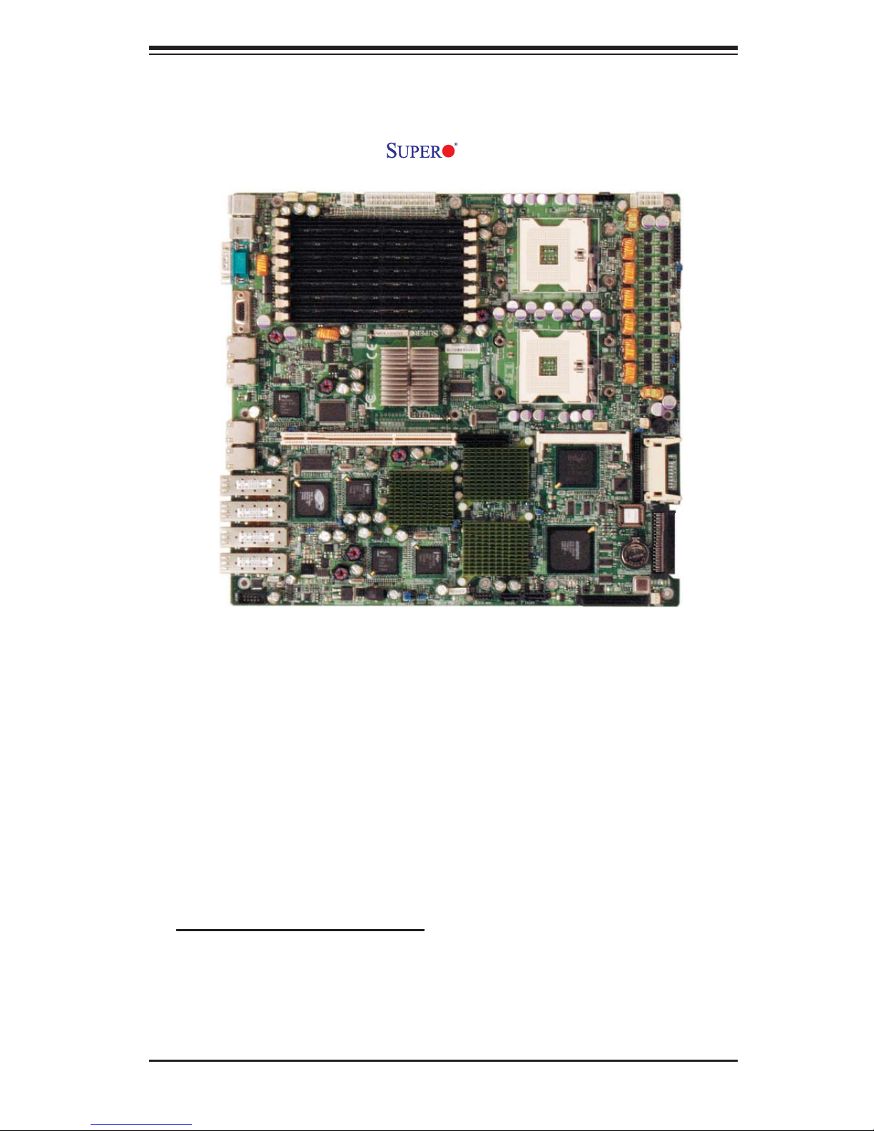
Figure 1-1. X6DHR-C8 Image
An Important Note to the User
• All images and layouts shown in this manual were based upon the latest PCB
Revision available at the time of publishing of this manual. The motherboard
you've received may or may not look exactly the same as the graphics shown
in this manual.
1-3
X6DHR-C8 User's Manual
Figure 1-2. X6DHR-C8 Motherboard Layout
(not drawn to scale)
KB/
Mouse
USB
0/1
COM1
VGA
JLAN1
JLAN2
JLAN3
JLAN4
COM2
JLAN5
JLAN6
JLAN7
JLAN8
Fan5
82546GB
PCI1
DA14
Fan6
UPER X6DHR-C8
S
Super
IO
PL1
J
AGE-
R
XL
JPG1
DA12
DA10
JWOL1
DA8
24-Pin
JPW2
4-Pin
PWR
DIMM
1A
(Bank 1)
DIMM 1B (Ban
DIMM 2A (Bank 2)
DIMM 2B (Bank 2)
DIMM 3
A
(Bank 3)
DIMM 3B (Bank 3)
DIMM 4A (Bank 4)
DIMM 4B (Bank 4)
PCI-X #1 100 MHz
82546GB
JPL2
82546GB
A
®
P
J
TX PWR
k
1)
E7520
indenhurst
L
North
(
Bridge)
Cavium
230 SL
1
82546GB
L3
PL4
J
J18
JPW1
SMBUS
J24
JUSB2
USB2/3
PCI-E x8
PXH
PC1
J
PXH
SATA0
J51
JPA1
SATA1
J52
CPU 1
CPU 2
IPMI
ICH5R
(South
Bridge)
7902
SCSI
CTRL
D
A2
JWOR1
Fan7
Fan8
DA1
JA2
J24
27
J
JIDE1
Clear
CMOS
BIOS
Batt
2
PA
J
JPA3
SCSI CH B
JP12
JL1
Fan3
ery
8-Pin
PWR
L
JPW3
Fan1
JF1
FP Ctrl
D1
J
JP15
E1
Fan2
JOH1
3
1
JP14
JP
Buzzer
Compact
Flash Card
Type 1
SCSI CH A
Fan4
Important Notes to the User
• All images and graphics shown in this manual were based upon the latest
PCB Revision available at the time of publishing of this manual. The motherboard you've received may or may not look exactly the same as the graphics
shown in this manual.
• See Chapter 2 for detailed information on jumpers, I/O ports and JF1 front
panel connections.
• " " indicates the location of "Pin 1".
• When the LE1 LED is on, the 5V Standby PWR is on. Maker sure to turn off
the power before installing or removing components.
• Refer to Page 2-7 for the Logical Port# of each onboard LAN.
1-4

Chapter 1: Introduction
Quick Reference ( X6DHR-C8)
(*Please refer to Chapter 2 for pin defi nitions and detailed
information.)
Jumper Description Default Setting
J18 Watch Dog Enable Pins 1-2 (Reset)
JP12 Power Fault (See Chapter 2)
JP13 3rd PWR Supply PWR Fault Detect On (Enabled)
JP14 Alarm Reset Enable Off (Disabled)
JP15 Reboot Option Off (Disabled)
JPA1 SCSI Channel A/B Enable On (Enabled)
JPA2/JPA3 SCSI Channels A/B Termination Off (Enabled)
JPC1 Cavium Pins 1-2 (Enabled)
JBT1 CMOS Clear See Chapter 2
JPG1 VGA Enable Pins 1-2 (Enabled)
JPL1/JPL2/JPL3/JPL4 JLAN (GLAN) 1-8 Enable Pins 1-2 (Enabled)
Connector Description
ATX PWR (JPW1) Primary ATX PWR Connector(*Also:JPW2, JPW3)
CPU PWR (JPW3) +12 V8-pin CPU PWR Connector (*required)
Aux. PWR (JPW2) +12V 4-pin (Auxiliary) system PWR Conn. (*Required)
COM1/COM2 COM1(JCOM1)/COM2(JCOM2) Serial Ports
DIMM#1A-DIMM#4B Memory (RAM) Slots
FAN 1-8 CPU/Chassis/OH Fan Headers(Fans7/8: CPU1/2 Fans)
IPMI (JIPMI) IPMI Connector
J22 System Management Bus Connector
J24 Power System Management (I
JD1 PWR LED(pins1-3)/SpeakerHeader (pins 4-7)
JF1 Front Control Panel Connector
IDE1, Compact Flash Slim IDE HDD Connector (JIDE1), Type 1 Compact
Flash Card Connector (JCOMP1)
JL1 Chassis Intrusion Header
JLAN 1-8 (*Note) G-bit Ethernet Ports (JLAN 1-4:RJ 45 ports, JLAN5-8:
SFP ports) (*SFP: Small Form Factor Pluggable)
JOH1 Overheat LED
JVGA1 VGA Connector
JWOL1 Wake-on-LAN Header
JWOR1 Wake-on-Ring Header
USB 0/1(JUSB1) (Back Panel) Universal Serial Bus Ports
USB 2/3 (JUSB2) Front Panel USB Headers
2
C) Connector
Indicator Description
LE1 Power LED
DA1/DA2 SCSI CH A LED (DA1)/SCSI CH B LED(DA2)
DA8/DA10/DA12/DA14 SPF LAN Activity LED Indicators
(*Note: Refer to Page 2-7 for the Logical Port# of each onboard LAN.)
1-5

X6DHR-C8 User's Manual
Motherboard Features
CPU
• Single or dual Intel® Xeon 64-bit 604-pin (NoconaTM w/EM64T) processors at
800 MHz front side (system) bus speed.
• Hyper-Threading (HT), EM64T supported
Using the EM64T Feature
• Use a CPU that supports the EM64T Technology
• Install a 64-bit OS (Windows XP Professional x64 Ed, Server 2003x64 Ed.)
• Install the 64-bit drivers for all MB components, devices and add-on cards
Using the Hyper-Threading (HT) Technology
• Use a CPU that supports Hyper-Threading Technology
• Install an OS that supports HT, including Windows XP/2003 Server and Linux
2.4x.
• Enable the HT feature in the BIOS (under "Advanced" Setting) before install-
ing a supported OS. (*Note: visit www.Intel.com for CPU support and driver
updates.)
Memory
• Eight 240-pin DIMM sockets supporting up to 16 GB Registered ECC DDR2-
400 (PC3200) SDRAM
(*Note: Interleaved memory requires memory modules to be installed in pairs.
See Section 2-3 for details.)
Chipset
• Intel E7520 Lindenhurst chipset
• ICH5R, PXH (X2), 82546GB (X4)
• National P87427 I/O chip
Expansion Slots
• One PCI-E slot (x8), or
• One PCI-X-100 slot
BIOS
• 8 Mb Phoenix
®
Flash ROM
• DMI 2.1, PCI 2.2, ACPI 2.0, Plug and Play (PnP), SMBIOS 2.3
PC Health Monitoring
• Onboard voltage monitors for CPU cores, chipset voltage, 3.3V, +5V, +3V
standby, +12V and -12V
• Fan status monitor with fi rmware/software on/off control
• CPU/chassis temperature monitors
• CPU 3-phase-switching voltage regulator
• Low noise fan speed control and System overheat/Fan Fail LED and control
• SuperDoctor III, NMI w/System resource alert via Supero Doctor III
• Environmental temperature monitoring via BIOS
1-6

Chapter 1: Introduction
• Power-up mode control for recovery from AC power loss
ACPI Features (optional)
• Slow blinking LED for suspend state indicator
• BIOS support for USB keyboard
• Main switch override mechanism
• Internal/external modem ring-on
Onboard I/O
• Support Adaptec 7902W dual channel Ultra 320 SCSI (Host RAID 0, 1, 10)
• One IPMI 2.0 socket
• Intel 82546GB dual Channel Gigabit Ethernet controller support up to 4 GLAN
ports and 4 GLAN ports w/4 Optical Small Form-Factor Pluggable GLAN
(SFP)
• One Slim IDE 44-pin connector and one Type 1 compact fl ash connector
• Two Fast UART 16550 compatible serial connections (1 port/1 header)
• PS/2 mouse and PS/2 keyboard ports
• Up to 4 USB 2.0 (Universal Serial Bus): 2 Front Panel USB ports, 2 Back
Panel USB Headers)
• Super I/O
• Two COM ports (1 header, 1 port)
• Two SATA ports support 2 drives (RAID 0, 1)
• VGA Connector (Vertical)
Other
• Internal/external modem ring-on (WOR)
• Wake-on-LAN (WOL)
• Console redirection
• SMBbus for SMC Power Supply
• Fan Speed Control via BIOS
CD/Diskette Utilities
• BIOS fl ash upgrade utility and device drivers
Dimensions
• ATX Ext. 12" x 13.05" (304.8 x 331.5 mm)
1-7
X6DHR-C8 User's Manual
Right
Gbit LAN1
ANVIK II
82546GB
IDSEL:PXH2_PBAD17
Gbit LAN2
ANVIK II
82546GB
IDSEL:PXH2_PAAD18
Gbit LAN3
ANVIK II
82546GB
IDSEL:PXH1_PBAD17
Gbit LAN4
ANVIK II
82546GB
IDSEL:PXH1_PAAD18
IDSEL:PXH1_PAAD17
IDSEL:PXH2_PBAD18
1 PCI-X
SLOT
JPCIX1
PCI-X BUS(100 MHZ)
PCI-X BUS(100 MHZ)
CAVIUM
CN1230SL
IDSEL:PXH2_PAAD17
PCI-X BUS(133 MHZ)
PCI-X BUS(100 MHZ)
SCSI
AIC7902W
UA24
Right
PCI-EXP
SLOTx8
JPCIE1
B
PXH
#2
A
U62
B
PXH
#1
A
U24
IDE
PRI/SEC
SATA
0, 1
USB PORT
0,1,2,3,4,5
PCI EXP.
PCI EXP.
PCI EXP.
UDMA/100
SATA
NOCONA PROCESSOR#1
NOCONA PROCESSOR#2VRM
X8
B
X8
C
A
X8
USB
CPU1
CPU2
MCH
U4E1
HUB
ICH5R
U6
CLOCK
DDRII-400
DDRII-400
PCI BUS(32-BIT)
BMC CON. FWHLPC I/O
U16 X3P1
4 DDR II 400
DIMMs
4 DDR II 400
LPC BUS
DIMMs
VGA
U10
Keyboard
Mouse
Floppy
COM2
H/WCOM1
MONITOR
Figure 1-9. Block Diagram of the E7520 Lindenhurst Chipset
Note: This is a general block diagram. Please see the previous Motherboard Features
pages for details on the features of the motherboard.
1-8

Chapter 1: Introduction
1-2 Chipset Overview
Built upon the functionality and the capability of the E7520 Lindenhurst chipset,
The X6DHR-C8 motherboard provides the performance and feature set required
for dual processor-based servers, with confi guration options optimized for commu-
nications, server security, storage, computation or database applications. The Intel
E7520 Lindenhurst chipset consists of the following components: the Lindenhurst
Memory Controller Hub (MCH), the 82801ER I/O Controller Hub 5-R (ICH5-R), and
the PCI-X Hub.
The E7520 Lindenhurst MCH supports single or dual Nocona processors with Front
Side Bus speeds of up to 800 MHz(*Note). Its memory controller provides direct
connection to two channels of registered DDR2 400 with a marched system bus
address and data bandwidths of up to 6.4GB/s. The Lindenhurst also supports the
new PCI Express high speed serial I/O interface for superior I/O bandwidth. The
MCH provides three confi gurable x8 PCI Express interfaces which may alternatively
be confi gured as two independent x4 PCI Express interfaces. These interfaces
support connection of the MCH to a variety of other bridges that are compliant
with the PCI Express Interface Specifi cation, Rev. 1.0a. The MCH interfaces with
the 82801ER I/O Controller Hub 5-R (ICH5R) via a dedicated Hub Interface sup-
porting a peak bandwidth of 266 MB/s using a x4 base clock of 66 MHz. The PXH
provides connection between a PCI Express interface and two independent PCI
bus interfaces that can be confi gured for standard PCI 2.3 protocol, as well as the
enhanced high-frequency PCI-X protocol. The PXH can be confi gured to support for
64-bit PCI devices running at 33 MHz, 66 MHz, 100 MHz, and 133 MHz.
The ICH5R I/O Controller Hub provides legacy support similar to that of previous
ICH-family devices, but with extensions in RAID 0,1 support, Serial ATA Technology,
and an integrated ASF Controller. In addition, the ICH5R also provides various inte-
grated functions, including a two-channel Ultra ATA/100 bus master IDE controller,
USB 2.0 host controllers, an integrated 10/100 LAN controller, an LPC fi rmware hub
(FWH) and Super IO interface, a System Management Interface, a power manage-
ment interface, integrated IOxAPIC and 8259 interrupt controllers.
(*Notes: The CPU FSB speed is set at 800 MHz by the Manufacturer. Please do
not change the CPU FSB setting.)
1-9

X6DHR-C8 User's Manual
1-3 PC Health Monitoring
This section describes the PC health monitoring features of the X6DHR-C8. The
motherboard has an onboard System Hardware Monitor chip that supports PC
health monitoring.
Onboard Voltage Monitors for the CPU Core, +3.3V, +5V, +3V
standby, +12V and −12V
The onboard voltage monitor will scan these voltages continuously. Once a volt-
age becomes unstable, it will give a warning or send an error message to the
screen. Users can adjust the voltage thresholds to defi ne the sensitivity of the
voltage monitor.
Fan Status Monitor with Firmware Speed Control
The PC health monitor can check the RPM status of the cooling fans. The onboard
fans are controlled by Thermal Management via BIOS.
CPU Overheat LED and Control
This feature is available when the user enables the CPU overheat warning function
in the BIOS. This allows the user to defi ne an overheat temperature. When this
temperature reaches the threshold, the CPU thermal trip feature will be activated
and it will send a signal to the Speaker LED and, at the same time, the CPU speed
will be decreased.
1-4 Power Confi guration Settings
This section describes features of your motherboard that deal with power and
power settings.
Slow Blinking LED for Suspend-State Indicator
When the CPU goes into a suspend state, the chassis power LED will start blinking
to indicate that the CPU is in suspend mode. When the user presses any key, the
CPU will wake-up and the LED will automatically stop blinking and remain on.
BIOS Support for USB Keyboard
If the USB keyboard is the only keyboard in the system, it keyboard will function
like a normal keyboard during system boot-up.
Main Switch Override Mechanism
When an ATX power supply is used, the power button can function as a system
suspend button. When the user depresses the power button, the system will enter
a SoftOff state. The monitor will be suspended and the hard drive will spin down.
1-10

Chapter 1: Introduction
Depressing the power button again will cause the whole system to wake-up. Dur-
ing the SoftOff state, the ATX power supply provides power to keep the required
circuitry in the system alive. In case the system malfunctions and you want to turn
off the power, just depress and hold the power button for 4 seconds. The power
will turn off and no power will be provided to the motherboard.
Wake Ring-On (WOR)
Wake-up events can be triggered by a device such as the external modem ringing
when the system is in the SoftOff state. Note that external modem ring-on can only
be used with an ATX 2.01 (or above) compliant power supply.
Wake-On-LAN (WOL)
Wake-On-LAN is defi ned as the ability of a management application to remotely
power up a computer that is powered off. Remote PC setup, up-dates and asset
tracking can occur after hours and on weekends so that daily LAN traffi c is kept to
a minimum and users are not interrupted. The motherboard has a 3-pin header
(WOL) to connect to the 3-pin header on a Network Interface Card (NIC) that has
WOL capability. Wake-On-LAN must be enabled in BIOS. Note that Wake-On-LAN
can only be used with an ATX 2.01 (or above) compliant power supply.
1-5 ACPI Features
ACPI stands for Advanced Confi guration and Power Interface. The ACPI specifi -
cation defi nes a fl exible and abstract hardware interface that provides a standard
way to integrate power management features throughout a PC system, including its
hardware, operating system and application software. This enables the system to
automatically turn on and off peripherals such as CD-ROMs, network cards, hard
disk drives and printers. This also includes consumer devices connected to the PC
such as VCRs, TVs, telephones and stereos.
In addition to enabling operating system-directed power management, ACPI pro-
vides a generic system event mechanism for Plug and Play and an operating
system-independent interface for confi guration control. ACPI leverages the Plug
and Play BIOS data structures while providing a processor architecture-independent
implementation that is compatible with both Windows and Linux Operating Sys-
tems.
1-11

X6DHR-C8 User's Manual
1-6 Power Supply
As with all computer products, a stable power source is necessary for proper and
reliable operation. It is even more important for processors that have high CPU
clock rates of 1 GHz and faster.
The
most power supplies generally meet the specifi cations required by the CPU, some
are inadequate. The X6DHR-C8 accommodates ATX power supplies. It is strongly
recommended that you use a high quality power supply that meets ATX power
supply Specifi cation 2.02 or above. Also your power supply must supply 1.5A for
the Ethernet ports. It must also be SSI compliant (info at http://www.ssiforum.org/).
Additionally, in areas where noisy power transmission is present, you may choose
to install a line fi lter to shield the computer from noise. It is recommended that
you also install a power surge protector to help avoid problems caused by power
surges. Please note that the 8-pin 12V (JWP3) and the 4-pin 12V (JPW2) power
connectors are also required to provide adequate power to you system.
X6DHR-C8 accommodates 12V ATX power supplies. Although
1-12

Chapter 2: Installation
Chapter 2
Installation
2-1 Static-Sensitive Devices
Electric-Static-Discharge (ESD) can damage electronic com ponents. To prevent
damage to your system board, it is important to handle it very carefully. The following
measures are generally suffi cient to protect your equipment from ESD.
Precautions
• Use a grounded wrist strap designed to prevent static discharge.
• Touch a grounded metal object before removing the board from the antistatic
bag.
• Handle the board by its edges only; do not touch its components, peripheral
chips, memory modules or gold contacts.
• When handling chips or modules, avoid touching their pins.
• Put the motherboard and peripherals back into their antistatic bags when not in
use.
• For grounding purposes, make sure your computer chassis provides excellent
conductivity between the power supply, the case, the mounting fasteners and
the motherboard.
• Use only the correct type of onboard CMOS battery. Do not install the onboard
upside down battery to avoid possible explosion.
Unpacking
The motherboard is shipped in antistatic packaging to avoid static damage. When
unpacking the board, make sure the person handling it is static protected.
2-1
X6DHR-C8 User's Manual
2-2 Processor and Heatsink Installation
When handling the processor package, avoid placing direct pressure
on the label area of the fan. Also, do not place the motherboard on a
!
IMPORTANT: Always connect the power cord last and always remove it before add-
ing, removing or changing any hardware components. Make sure that you install
the processor into the CPU socket before you install the CPU (CEK) heat sink.
CPU Installation
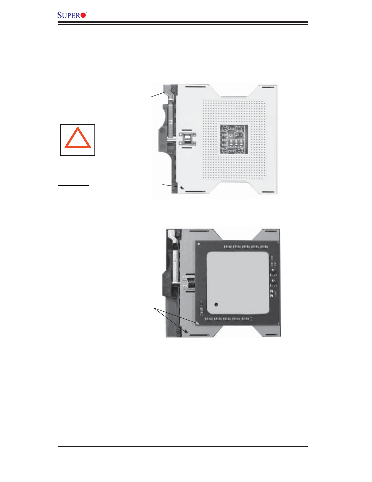
1. Lift the lever on the CPU socket: lift
the lever completely as shown on the
picture on the right; otherwise, you
will damage the CPU socket when
power is applied. (Install CPU1 fi rst.)
conductive surface, which can damage the BIOS battery and prevent
the system from booting up.
2. Insert the CPU in the socket, mak-
ing sure that pin 1 of the CPU aligns
with pin 1 of the socket (both corners
are marked with a triangle). When
using only one CPU, install it into CPU
socket #1 (socket #2 is automatically
disabled if only one CPU is used).
3. Press the lever down until you
hear the *click* so you can be
sure that the CPU is securely
installed in the CPU socket.
Socket lever
Pin1
Pin 1
Socket lever in the
locking Position
2-2
Chapter 2: Installation
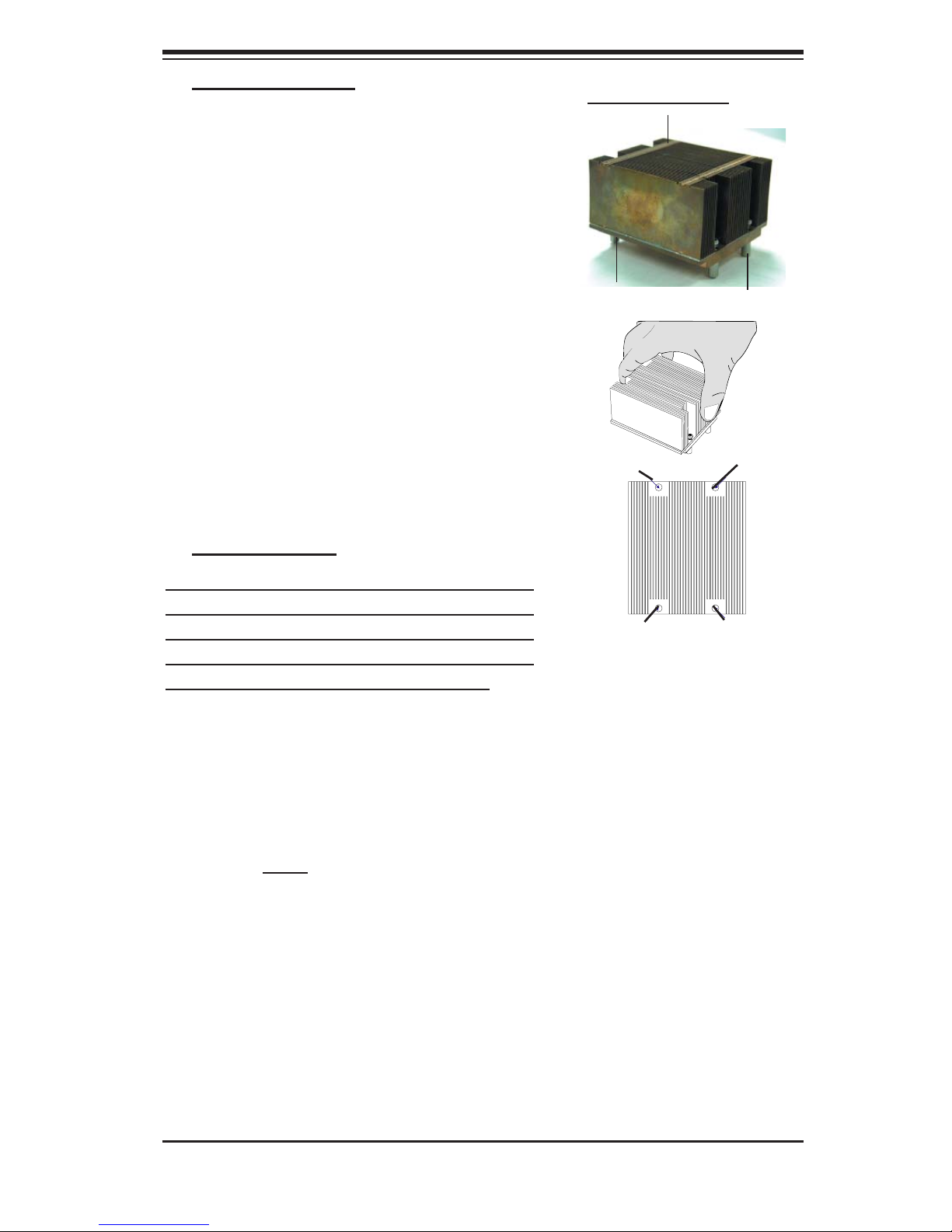
Heatsink Installation
1. Do not apply any thermal compound to
the heatsink or the CPU die-the required
amount has already been applied.
2. Place the heatsink on top of the CPU so
that the four mounting holes are aligned
with those on the retention mechanism.
3. Screw in two diagonal screws (ie the #1
and the #2 screws) until just snug (-do not
fully tighten the screws to avoid possible
damage to the CPU.)
4. Finish the installation by fully tightening all
four screws.
Intel CEK Heatsink
Screw#1
Screw#1
Screw#2
Screw#3
Heatsink Removal
(Caution! We do not recommend that the CPU or
the heatsink be removed. However, if you do need
to un-install the heatsink, please follow the instruc-
tions below to remove the heatsink to prevent dam-
age done to the CPU or the CPU socket. )
1. Unscrew and remove the heatsink screws
from the motherboard in the sequence as show
in the picture on the right.
2. Hold the heatsink as show in the picture on the
right and gently wriggle the heatsink to loosen it
from the CPU. (Do not use excessive force when
wriggling the heatsink!!)
3. Once the CPU is loosened from the heatsink,
remove the heatsink from the CPU socket.
Screw#4
Screw#2
4. Clean the surface of the CPU and the heatsink
to get rid of the old thermal grease. Reapply the
proper amount of thermal grease on the surface
before you reinstall the CPU and the heatsink.
2-3
X6DHR-C8 User's Manual
Figure 2-1. PGA 604 Socket: Empty and with Processor Installed
Empty socket
!
Warning! Make
sure you lift the lever
completely when
installing the CPU.
If the lever is only
partly raised, damage
to the socket or CPU
may result.
Lever
Triangle
Processor
(installed)
Mounting the Motherboard in the Chassis
All motherboards have standard mounting holes to fi t different types of chassis.
Make sure the location of all the mounting holes for both the motherboard and
the chassis match. Although a chassis may have both plastic and metal mounting
fasteners, metal ones are highly recommended because they ground the moth-
erboard to the chassis. Make sure the metal standoffs click in or are screwed in
tightly. Then use a screwdriver to secure the motherboard onto the motherboard
tray. (*Note: some components are near to the mounting holes. Please take all
necessary precautionary measures to prevent damage done to these components
when installing the motherboard into the chassis.)
Triangle
2-4
Chapter 2: Installation
2-3 Installing DDR 2 Memory
Memory Module Installation (See Figure 2-2)
Exercise extreme care when installing or removing memory modules
to prevent any possible damage.
1. Insert each DDR 2 memory module vertically into its slot. Pay attention to the
notch along the bottom of the module to prevent inserting the module incor-
rectly. (See support information below.)
2. Gently press down on the memory module until it snaps into place.
Support
The X6DHR-C8 supports Dual channel, ECC Registered, interleaved, DDR 2
400 SDRAM. (Populating DIMM#1A,DIMM#1B, and/or DIMM#2A, DIMM#2B
with memory modules of the same size and of the same type will result in dual
channel, two-way interleaved memory which is faster than the single channel,
non-interleaved memory.
To Install:
Insert module
vertically and
press down
until it snaps
into place.
Pay attention
to the alignment notch at
the bottom.
Figure 2-2. Installing and Removing DIMMs
Notch
Release
Tab
Note: Notch
should align
receptive point
DDRII
with the
on the slot
II
Notch
Release
Tab
To Remove:
Use your thumbs to gently push near the edge of both ends of the
module. This should release it from the slot.
2-5

X6DHR-C8 User's Manual
2-4 A. I/O Ports and Front Panel Control Connectors
The I/O ports are color coded in conformance with the PC 99 specifi cation. See
Figure 2-3 below for the colors and locations of the various I/O ports.
Figure 2-3. I/O Port Locations and Defi nitions
(Green)
Mouse
JLAN6 JLAN8
KB
(Purple)
USB 0/1
COM1
(Turquoise)
VGA
JLAN1
JLAN2 JLAN3 JLAN4 JLAN5
JLAN7
Front Control Panel
JF1 contains header pins for various buttons and indicators that are normally located
on a control panel at the front of the chassis. These connectors are designed specifi -
cally for use with Supermicro server chassis. See Figure 2-4 for the descriptions of
the various control panel buttons and LED indicators. Refer to the following section
for descriptions and pin defi nitions.
Figure 2-4. JF1 Header Pins
1920
Ground
X
Power LED
NMI
X
Vcc
OH/Fan Fail LED
Power Fail LED
HDD LED
NIC1 LED
NIC2 LED
Ground
Ground
2
2-6
Vcc
Vcc
Vcc
Vcc
Vcc
Reset
Pwr
1
Reset Button
Power Button
Chapter 2: Installation
JLAN1
®
S
UPER X6DHR-C8
JLAN
2
DIMM 2B (Bank 2)
DIMM 2A (Bank 2)
DIMM 3B (B
ank 3)
DIMM 3A (B
ank 3)
DIMM 4B
(B
ank 4)
DIMM 4A (Bank 4)
DIMM 1A
(Bank 1
)
DIMM 1B (Bank 1
)
Fan1
JF1
FP Ctrl
J
D1
JP15
Fan2
J
OH
1
Fan3
JL1
IPMI
JIDE1
BIOS
J18
J
PA1
SCSI CH
A
SCSI CH B
Fan4
7902
CTRL
SATA0
SATA1
USB2/3
SMBUS
Buzzer
JWOR1
Battery
JP
L1
R
AGE-
XL
PCI-X #1
1
00 MHz
Super
IO
(North
Bridge)
JPG1
COM1
USB
0/1
KB/
Mouse
Fan5
Fan6
ATX PW
R
4-Pin
PWR
24-Pin
Fan7
J24
JP12
Fan8
SCSI
CPU 1
PXH
PCI-E x8
COM2
JPA2
JPA3
DA1
DA2
ICH5R
PXH
Lindenhurst
Clear
CMOS
(South
Bridge)
E7520
JLAN3
JLAN4
JLAN5
Cavium
1230 SL
JPL3
JPL4
J
PL
2
JA2
J27
JPW3
J
PW1
J
PW2
JPC1
DA10
DA12
JWOL1
DA8
DA14
CPU 2
VG
A
8-Pin
PWR
JP14
JP13
LE
1
JUSB2
J51
J52
J24
PCI1
82546GB
82546GB
82546GB
82546GB
JLAN6
JLAN7
JLAN8
Compact
Flash Card
Type 1
2-4 B. Logical Port Numbers for the Onboard LANs
Sequence of Hardware/BIOS Scan of the Onboard LANs
Phyical
JLAN1 JLAN2 JLAN3 JLAN4 JLAN5 JLAN6 JLAN7 JLAN8
Port#
Logical
eth6 eth7 eth4 eth5 eth3 eth2 eth1 eth0
Port#
(*Note: The Logical Port Numbers for the Onboard LAN ports vary depending
on the version of the OS installed in the system. The Logical Port Numbers
shown above are based upon Redhat Kernel 2.6.9 and Kernel 2.4.21.)
Physical JLAN Ports #1-#8
2-7

X6DHR-C8 User's Manual
2-5 Connecting Cables
ATX Power Connector
The main power supply connector on
the X6DHR-C8 meets the SSI (Su-
perset ATX) 24-pin specifi cation. You
must also connect the 4-pin (JPW2)
power connector to your power supply
to provide adequate power supply for
system power consumption. See the
table on the right for pin defi nitions.
Processor Power Connector
In addition to the Primary ATX and the
Auxiliary power connectors (above),
the 12V 8-pin Processor connector
at JPW3 must also be connected to
your power supply for CPU power
consumption.
ATX Power 24-pin Connector
Pin Defi nitions (JPW1)
Pin# Defi nition Pin # Defi nition
13 +3.3V 1 +3.3V
14 -12V 2 +3.3V
15 COM 3 COM
16 PS_ON 4 +5V
17 COM 5 COM
18 COM 6 +5V
19 COM 7 COM
20 Res (NC) 8 PWR_OK
21 +5V 9 5VSB
22 +5V 10 +12V
23 +5V 11 +12V
24 COM 12 +3.3V
4-Pin 12V Connector
Pin Defi nitions (JPW2)
Pins Defi nition
1 & 2 Ground
3 & 4 +12V
8-Pin 12V Connector
Pin Defi nitions (JPW3)
Pins Defi nition
1 through 4 Ground
5 through 8 +12V
(*Required)
(*Required)
KB/
Mouse
USB
0/1
VG
JLAN1
JLAN2
JLAN3
COM1
A
JLAN4
JLAN5
JLAN6
JLAN7
JLAN8
COM2
Fan5
82546GB
PCI1
DA14
JWOL1
DA8
4-pin PWR
Fan6
JPW2
4-Pin
PWR
UPER X6DHR-C8
S
Super
IO
JPL1
RAGEXL
PG1
J
DA12
DA10
ATX 24-pin PWR
A
24-Pin
DIMM 1A (B
DIMM 1B (Bank
DIMM 2
DIMM 2B (Bank 2)
DIMM 3A (Bank 3)
DIMM 3B (Bank 3)
DIMM 4
DIMM 4B (Bank 4)
A (Bank 2)
A (Bank 4)
PCI-X #
82546GB
JPL2
82546GB
ank 1)
®
1 100 MHz
PL
J
TX PWR
E7520
inden
L
(North
Bridge)
1230 SL
82546GB
3
J
J18
JPW1
1)
hurst
Cavium
PL4
SMBUS
24
J
JUSB2
USB2/3
PCI-E x8
JPC1
PXH
PXH
SATA0
51
J
JPA1
SATA1
52
J
CPU 1
CPU 2
IPMI
ICH5R
(South
Bridge)
7902
SCSI
CTR
DA2
JWOR1
Fan7
Fan8
L
DA1
JA2
8-pin PWR
8-Pin
PWR
P12
J24
J
LE1
JL1
Fan3
27
J
JIDE1
Clear
CMOS
BIOS
ery
Batt
2
JPA
A3
P
J
SCSI CH B
JPW3
Fan1
JF1
FP Ctrl
5
JD1
JP1
Fan2
JOH1
13
P
JP14
J
Buzzer
Compact
Flash Card
Type 1
SCSI CH A
Fan4
2-8
Chapter 2: Installation
n
n
NMI Button
The non-maskable interrupt button
header is located on pins 19 and 20
of JF1. Refer to the table on the right
for pin defi nitions.
Power LED
The Power LED connection is located
on pins 15 and 16 of JF1. Refer to the
table on the right for pin defi nitions.
NMI Button
Pin Defi nitions (JF1)
Pin# Defi nition
19 Control
20 Ground
Power LED
Pin Defi nitions (JF1)
Pin# Defi nition
15 Vcc
16 Control
KB/
Mouse
USB
0/1
VG
COM1
JLAN1
JLAN2
JLAN3
JLAN4
COM2
A
JLAN5
JLAN6
JLAN7
JLAN8
Fan5
Fan6
UPER X6DHR-C8
S
82546GB
Super
IO
JPL1
PCI1
DA14
AGE-
R
XL
PG
J
DA12
DA10
WOL1
J
DA8
JPW2
4-Pin
PWR
DIMM
DIMM
DIMM 2A (B
DIMM 2B (Bank 2)
DIMM 3
DIMM 3B (Bank 3)
DIMM 4A (B
DIMM 4B (Bank 4)
1
R
ATX PW
24-Pin
1A (B
ank
1
)
1
B (Bank
1
)
ank 2)
A (B
ank 3)
ank 4)
®
E7520
Linden
orth
N
(
Bridge)
PCI-X #1 100 MHz
Cavium
82546GB
JPL2
1230 SL
82546GB
82546GB
3
JPL
JPL
J1
8
JPW1
hurst
4
SMBUS
J24
PCI-E x8
1
PC
J
USB2
J
USB2/3
PXH
PXH
SATA0
J51
JP
A1
SATA1
J52
CPU 1
CPU 2
ICH5R
(South
Bridge)
7902
SCSI
CTRL
D
A
2
PWR LED
2
8-Pin
Fan7
PWR
P1
IPMI
JWOR1
JA2
DA1
Fan8
J24
Clear
CMOS
A
JP
JP
SCSI CH B
JPW3
J
Fan1
JF1
FP Ctrl
5
JD1
JP1
1
LE
Fan2
JOH1
4
3
JP1
JP1
JL1
Fan3
J27
Buzzer
JIDE1
Compact
Flash Card
Type 1
BIOS
A
Battery
SCSI CH
2
3
A
Fan4
2-9
Ground
Power LED
HDD LED
NIC1 LED
NIC2 LED
OH/Fan Fail LED
Power Fail LED
X
Ground
Ground
NMI
1920
NMI
X
Vcc
Vcc
Vcc
Vcc
Vcc
Vcc
Reset
Reset Butto
Power Butto
Pwr
1
2
X6DHR-C8 User's Manual
HDD LED
The HDD LED connection is located
on pins 13 and 14 of JF1. Attach the
hard drive LED cable here to display
disk activity (for any hard drives on
the system, including SCSI, Serial ATA
and IDE). See the table on the right
for pin defi nitions.
NIC1/NIC2 LED Indicators
The NIC (Network Interface Control-
ler) LED connections for the GLAN
Port1 is located on pins 11 and 12
of JF1, and for the GLAN Port2 is
located on pins 9 and 10 of JF1. At-
tach the NIC LED cables to display
network activity. Refer to the tables
on the right for pin defi nitions.
HDD LED
Pin Defi nitions (JF1)
Pin# Defi nition
13 Vcc
14 HD Active
NIC1 LED
Pin Defi nitions (JF1)
Pin# Defi nition
11 Vcc
12 Ground
NIC2 LED
Pin Defi nitions (JF1)
Pin# Defi nition
9 Vcc
10 Ground
KB/
Mouse
USB
0/1
VGA
JLAN1
JLAN2
COM1
JLAN3
JLAN4
JLAN5
JLAN6
JLAN7
JLAN8
COM2
Fan5
Fan6
UPER X6DHR-C8
S
82546GB
Super
IO
JPL1
PCI1
DA14
AGE-
R
XL
PG
J
DA12
DA10
L1
WO
J
DA8
24-Pin
JPW2
4-Pin
PWR
DIMM 1A
(B
DIMM 1B (Bank
DIMM 2A (B
DIMM 2B (Bank 2)
DIMM 3
A (B
DIMM 3B (Bank 3)
DIMM 4A (B
DIMM 4B (Bank 4)
®
PCI-X #1 100 MHz
82546GB
JPL2
1
82546GB
JPL
ATX PWR
ank
ank 2)
ank 3)
ank 4)
E7520
Linden
3
J1
JPW1
1
)
1
)
orth
N
(
Bridge)
Cavium
1230 SL
82546GB
4
JPL
8
hurst
SMBUS
J24
J
USB2/3
PCI-E x8
1
PC
J
USB2
PXH
PXH
SATA0
J51
JP
SATA1
J52
CPU 1
CPU 2
A1
D
A
IPMI
ICH5R
(South
Bridge)
7902
SCSI
CTRL
2
JWOR1
JA2
DA1
Fan7
Fan8
J24
Clear
CMOS
BIOS
Battery
2
A
JP
3
A
JP
SCSI CH B
2
P1
J
JL1
Fan3
J27
JIDE1
2-10
8-Pin
PWR
5
JP1
1
LE
Compact
JPW3
Fan1
JF1
FP Ctrl
D1
J
Fan2
JOH1
4
3
JP1
JP1
Buzzer
Flash Card
Type 1
A
SCSI CH
Fan4
HDD NIC1/NIC2 LED
1920
Ground
X
Power LED
HDD LED
NIC1 LED
NIC2 LED
OH/Fan Fail LED
Power Fail LED
Ground
Ground
1
2
NMI
X
Vcc
Vcc
Vcc
Vcc
Vcc
Vcc
Reset
Pwr
Reset Button
Power Button
Overheat/FanFail LED
Connect an LED to the OH/Fan Fail
connection on pins 7 and 8 of JF1 to
provide advanced warning of chas-
sis overheating or sytem fan failure.
Refer to the table on the right for pin
defi nitions.
Power Fail LED
The Power Fail LED connection is
located on pins 5 and 6 of JF1. Re-
fer to the table on the right for pin
defi nitions.
OH/Fan Fail LED
Pin Defi nitions (JF1)
Pin# Defi nition
7 Vcc
8 HD Active
PWR Fail LED
Pin Defi nitions (JF1)
Pin# Defi nition
5 PWR Fail LED-
6 PWR Fail LED+
PWR Fail Indicator Status
State Defi nition
Green PWR On, System
Amber Redundant PWR
Chapter 2: Installation
OH/Fan Fail Indicator
Status
State Defi nition
Off Normal
On Overheat
Flashing Fan Fail
Normal
Failure
KB/
Mouse
USB
0/1
VGA
JLAN1
JLAN2
COM1
JLAN3
JLAN4
JLAN5
JLAN6
JLAN7
JLAN8
COM2
Fan5
82546GB
DA14
PCI1
J
WO
DA8
Fan6
JPL1
DA12
DA10
S
AGE-
R
XL
PG
J
L1
ATX PWR
24-Pin
(B
A (B
82546GB
82546GB
JPW1
ank
1
)
1
)
ank 2)
ank 3)
ank 4)
®
E7520
hurst
Linden
orth
N
(
Bridge)
Cavium
1230 SL
82546GB
3
JPL
4
JPL
J1
8
JPW2
4-Pin
PWR
DIMM 1A
DIMM 1B (Bank
DIMM 2A (B
DIMM 2B (Bank 2)
DIMM 3
DIMM 3B (Bank 3)
DIMM 4A (B
DIMM 4B (Bank 4)
UPER X6DHR-C8
Super
IO
PCI-X #1 100 MHz
JPL2
1
SMBUS
J24
PCI-E x8
1
PC
J
USB2
J
USB2/3
PXH
PXH
SATA0
J51
JP
SATA1
J52
CPU 2
A1
D
CPU 1
IPMI
ICH5R
(South
Bridge)
7902
SCSI
CTRL
A
2
JWOR1
DA1
JA2
Fan7
Fan8
J24
J27
Clear
CMOS
BIOS
Battery
2
A
JP
3
A
JP
SCSI CH B
2
8-Pin
PW
P1
J
LE
JL1
Fan3
JIDE1
Compact
2-11
R
JPW3
Fan1
JF1
FP Ctrl
5
D1
J
JP1
1
Fan2
JOH1
4
3
JP1
JP1
Buzzer
Flash Card
Type 1
A
SCSI CH
Fan4
OH/Fan Fail LED
PWR Fail LED
1920
Ground
X
Power LED
HDD LED
NIC1 LED
NIC2 LED
OH/Fan Fail LED
Power Fail LED
Ground
Ground
1
2
NMI
X
Vcc
Vcc
Vcc
Vcc
Vcc
Vcc
Reset
Pwr
Reset Button
Power Button
 Loading...