

Supermicro SUPER P6DNH2, SUPER P6DNH User Manual

SUPER
®
Dual Pentium Pro Processor
®
SUPER P6DNH
SUPER P6DNH2
USER’S MANUAL
Revision 1.1

The information in this User’s Manual has been carefully reviewed and is believed to be
accurate. The vendor assumes no responsibility for any inaccuracies that may be
contained in this document, makes no commitment to update or to keep current the
information in this manual, or to notify any person or organization of the updates.
SUPERMICRO COMPUTER reserves the right to make changes to the product described in
this manual at any time and without notice. This product, including software, if any, and
documentation may not, in whole or in part, be copied, photocopied, reproduced, translated
or reduced to any medium or machine without prior written consent.
IN NO EVENT WILL SUPERMICRO COMPUTER BE LIABLE FOR DIRECT, INDIRECT,
SPECIAL, INCIDENTAL, OR CONSEQUENTIAL DAMAGES ARISING FROM THE USE OR
INABILITY TO USE THIS PRODUCT OR DOCUMENTATION, EVEN IF ADVISED OF THE
POSSIBILITY OF SUCH DAMAGES. IN PARTICULAR, THE VENDOR SHALL NOT HAVE
LIABILITY FOR ANY HARDWARE, SOFTWARE, OR DATA STORED OR USED WITH THE
PRODUCT, INCLUDING THE COSTS OF THE REPAIRING, REPLACING, OR
RECOVERING SUCH HARDWARE, SOFTWARE, OR DATA.
Unless you request and receive written permission from SUPERMICRO COMPUTER, you
may not copy any part of this document.
Information in this document is subject to change without notice. Other products and
companies referred to herein are trademarks or registered trademarks of their respective
companies or mark holders.
Copyright © 1997 by SUPERMICRO COMPUTER INC.
All rights reserved.
Printed in the United States of America.

Preface
About This Manual
This manual is written for system houses, PC technicians and
knowledgeable PC end users. It provides information for the installation and use of the SUPER® P6DNH/P6DNH2 motherboard, which
supports the 200/180/166/150, >200 MHz Intel® Pentium® Pro processors, and the i960® RP IO processor.
The Pentium Pro processor has two 64-bit data buses. One bus
interconnects to the built-in L2 cache and the other is an external
bus that interconnects with the system memory, I/O and the other
processor. Both come with ECC (Error Checking and Correction)
allowing for the correction of single-bit data errors and detection of
2-bit errors on the data bus.
Manual Organization
Chapter 1, Introduction, describes the features, specifications and
performance of the SUPER P6DNH/P6DNH2 system board, provides detailed information about the chipset, and offers warranty
information.
Refer to Chapter 2, Installation, for a list of the equipment needed
for a system based on the SUPER P6DNH/P6DNH2 system board.
This chapter provides you with the instructions for handling staticsensitive devices, checking and/or configuring the jumpers. Read
this chapter when you want to install or remove SIMM memory modules and to mount the system board in the chassis. Also refer to
this chapter to connect the floppy and hard disk drives, USB, IDE
interface, parallel port, serial ports, as well as the cables for the
power supply, reset cable, Keylock/Power LED, speaker and keyboard.
iii

SUPER P6DNH/P6DNH2 User's Manual
If you encounter any problem, please see Chapter 3, Troubleshooting, which describes troubleshooting procedures for video, memory, and the setup configuration stored in memory. Instructions are
also included on contacting a technical assistance support representative and returning merchandise for service and the BBS# for
BIOS upgrades .
iv

Preface
Table of Contents
Preface
About This Manual ......................................................................................... iii
Manual Organization...................................................................................... iii
Chapter 1:
1-1 Overview............................................................................................... 1-1
SUPER P6DNH/P6DNH2 Motherboard Layout ...................... 1-4
SUPER P6DNH/P6DNH2 System Board Architecture.......... 1-5
Features......................................................................................... 1-6
1-2 Power Supply ...................................................................................... 1-8
1-3 Chipset Overview................................................................................ 1-8
1-4 National Semiconductor 87306 ....................................................... 1-9
1-5 Voltage Regulator Modules .............................................................. 1-9
1-6 System Overheat Thermal Control ................................................1-10
1-7 Warranty, Technical Support, and Service .................................. 1-11
Parts.............................................................................................. 1-11
BIOS .............................................................................................. 1-11
Labor............................................................................................. 1-11
Returns......................................................................................... 1-11
Chapter 2: Installation
2-1 SUPER P6DNH/P6DNH2 System Components.......................... 2-1
Standard System Configuration ................................................ 2-1
Enhanced System Configuration .............................................. 2-2
2-2 Static-Sensitive Devices ................................................................... 2-2
Precautions ................................................................................... 2-2
Unpacking...................................................................................... 2-3
2-3 Configuring System Board Jumpers.............................................. 2-3
Manufacturing Settings ............................................................... 2-3
v

SUPER P6DNH/P6DNH2 User's Manual
Changing the CPU Speed ......................................................... 2-4
2-4 Mounting the Motherboard in the Chassis ................................... 2-4
2-5 Connecting Cables ............................................................................ 2-4
Power Supply Connectors.......................................................... 2-5
Turbo Function.............................................................................. 2-5
USB Connectors........................................................................... 2-7
Reset Cable Connector .............................................................. 2-8
Keylock/Power LED Cable Connector ..................................... 2-8
Keyboard Connector .................................................................... 2-9
Thermal Control Connector ....................................................... 2-9
Hard Drive LED .......................................................................... 2-10
Speaker Cable Connector........................................................ 2-10
PS/2 Keyboard and Mouse Ports ........................................... 2-11
Back-up Cooling Fan and Buzzer Connectors ..................... 2-12
Serial Ports.................................................................................. 2-12
2-6 Installing/Removing the SIMM Modules ...................................... 2-13
SIMM Module Installation .......................................................... 2-13
Removing SIMM Modules ......................................................... 2-14
2-7 Connecting Floppy and Hard Disk Drives .................................. 2-15
Parallel Port Connector ............................................................ 2-16
Floppy Connector ....................................................................... 2-17
IDE Interfaces ............................................................................. 2-18
Chapter 3: Troubleshooting
3-1 Troubleshooting Procedures ........................................................... 3-1
No Video ........................................................................................ 3-1
Troubleshooting Flowchart ........................................................ 3-2
Memory Error ................................................................................. 3-3
Losing the System’s Setup Configuration.............................. 3-3
3-2 Technical Support Procedures........................................................ 3-4
3-3 Returning Merchandise for Service................................................ 3-4
vi

Table of Contents
vii

SUPER P6DNH/P6DNH2 User's Manual
viii

Chapter 1: Introduction
Chapter 1
Introduction
1-1 Overview
SUPER P6DNH/P6DNH2 is a high performance, I2OΤΜ enabled computer system board based on Intel® Pentium® Pro 200/180/166/150
MHz processors. They incorporate Intel's 440FX chipset and support dual processing. SUPER P6DNH uses the 33 MHz i960® RP I/
O processor while SUPER P6DNH2 uses the 66 MHz i960 RD I/O
processor.
The Pentium Pro processor is Intel’s top-of-the-line generation of
performance for servers, workstations, and high-end desktops. It
delivers its superior performance through its Dynamic Execution
microarchitecture which allows multiple branch prediction, dataflow
analysis and speculative execution.
The Pentium Pro processor includes 16KB of internal cache and an
integrated 256KB or 512KB non-blocking secondary cache in the
same package. Having the L2 cache inside the package will not
only save space, it will also have the CPU core communicating with
the L2 cache at full speed. Non-blocking means that the transactions on the processor bus do not block subsequent bus transactions. For example, when a cache miss occurs, the processor will
continue to process other instructions while initiating a bus transaction to satisfy the cache miss. These instructions could generate
additional cache misses which could cause more bus transactions.
The Pentium Pro processor can maintain up to four concurrent requests of the bus.
The general purpose registers of the Pentium Pro processor are
the same as on previous generations. The processor bus achieves
high bus efficiency by providing support for multiple, pipelined
transactions and deferred replies. A single processor may have up
to 4 outstanding transactions at the same time. There are a variety
1-1

SUPER P6DNH/P6DNH2 User’s Manual
of wider datapaths both inside and outside the chip. It has an
external 64-bit bus in order to communicate more efficiently with the
system memory. The package have two cavities with about 21 million transistors. The larger one is the CPU core with 5.5 million
transistors. The smaller one is the non-blocking cache which contains 15.5 million transistors.
The i960 RP/RD I/O processor is a highly integrated intelligent I/O
subsystem on a chip. Mode 3 is the default setting for its normal
operation. The i960 RP/RD has two main functions. As a local
processor, it offloads interrupt-intensive I/O tasks from the host
CPU. Its architecture is composed of a RISC core surrounded by
peripherals essential to the I/O function. The on-board PCI-to-PCI
bridge enables designers to connect I/O components directly to the
PCI bus and also add additional PCI slots. The bridge improves
overall system performance by reducing bus traffic. SUPER
P6DNH/P6DNH2 supports four primary and four secondary PCI
buses.
I2O is an open software-interface standard for I/O devices, independent of the specific device and operating system. It is implemented
on the i960 RP/RD I/O processor. With I2O, I/O hardware vendors
do not have to write drivers in countless variation, one for each
operating system version.
To attain portability across multiple operating systems and host
platforms, I2O drivers are divided into the OS Services Module
(OSM), and Hardware Device Module (HDM). The first module interfaces with the host operating system. The second interfaces with
the particular device, media or server managed by the driver. The
two modules interface with each other through a two-layered communications system. A Message Layer sets up a communications
session. A Transport Layer defines how information will be shared.
The Message Layer resides on the Transport Layer.
Peripheral Component Interconnect (PCI) provides industry-leading
performance and compatibility. The 32-bit, 33 MHz pathway to the
CPU offers performance unmatched by other bus architectures. The
1-2

Chapter 1: Introduction
PCI standard is clearly defined to ensure complete compatibility. A
PCI add-on card available today will work in any PC-compliant system in the future. The PCI add-on card interface is processor independent. This will enable an efficient transition to future processor
generations and use with multiple processor architecture.
In addition to the security of a true standard, PCI add-on cards feature auto-configurability for easy integration. The user-friendly BIOS
automatically allocates system resources for add-on cards and configures hard disk, memory, and other peripherals. No more
hassles with settings, jumpers, or switches. Just plug in the card
and go (Plug and Play or PnP).
The motherboard’s eight 32-bit slots with industry standard PCI design have a very high performance capability that provides an ideal
system board solution for a wide range of demanding applications;
such as networking multiuser environments, computer aided
design (CAD), computer aided manufacturing (CAM), computeraided engineering (CAE), database management, desktop publishing, image processing, and artificial intelligence. The
motherboard’s additional three ISA slots provide standard 16-bit
compatibility for AT-type add-on card expansion.
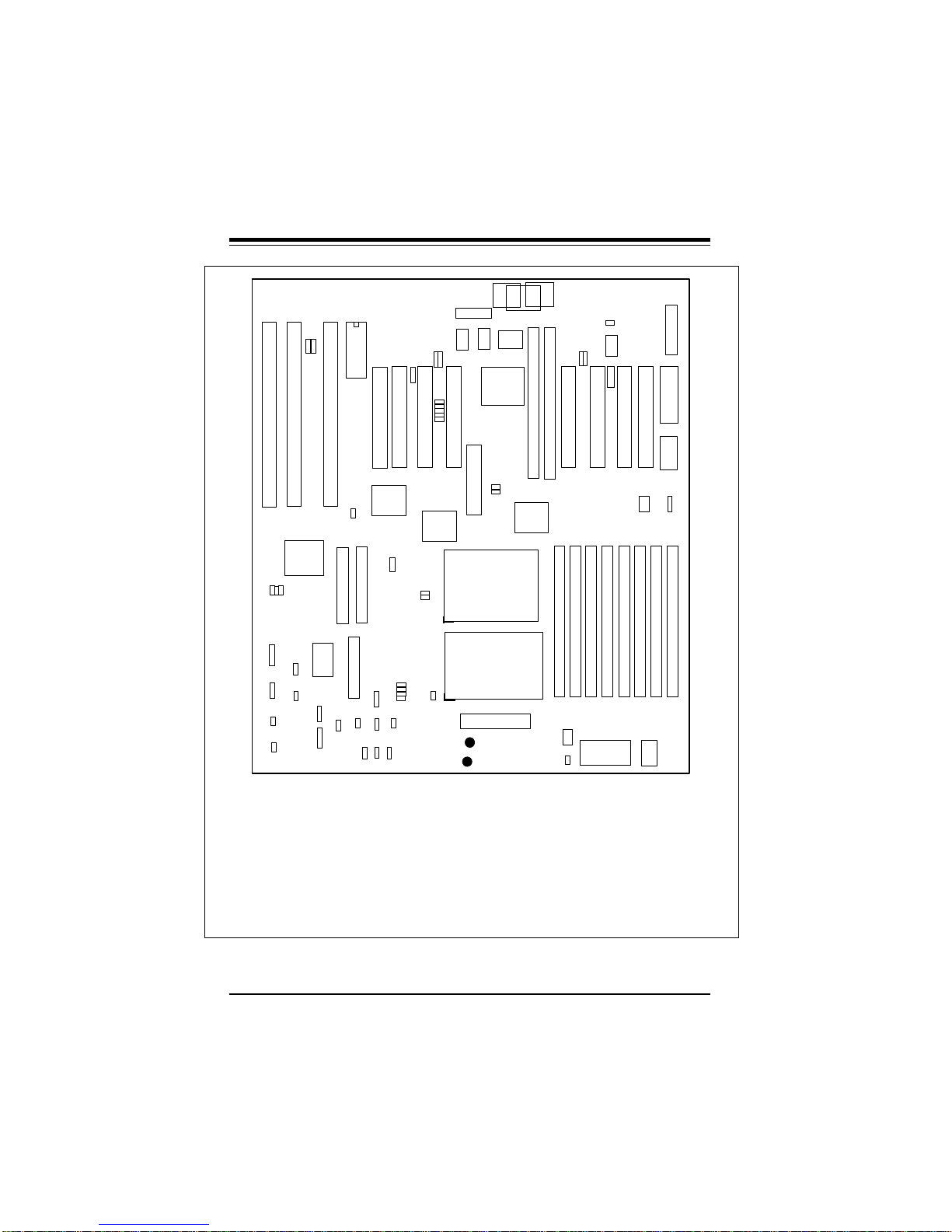
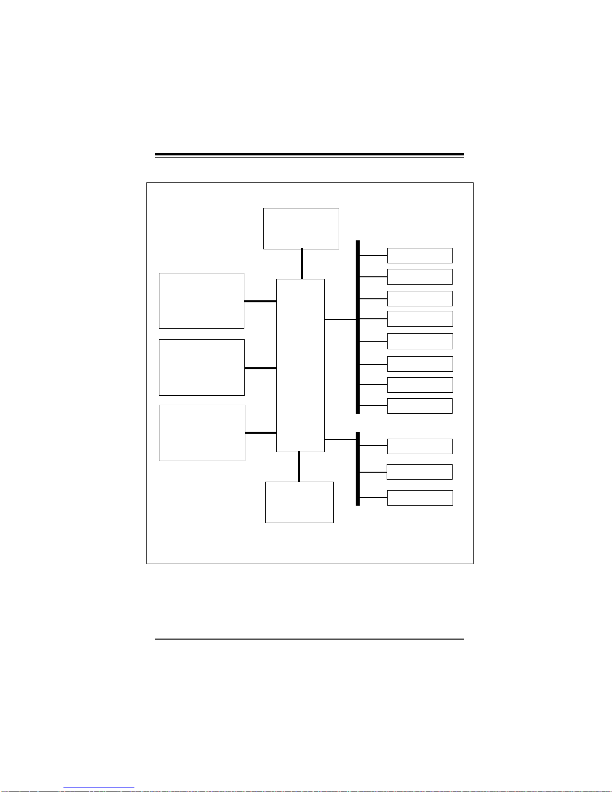
Figure 1-1 shows the layout of the SUPER P6DNH/P6DNH2
motherboard. Figure 1-2 shows the architecture of the SUPER
P6DNH/P6DNH2 motherboard.
1-3
SUPER P6DNH/P6DNH2 User’s Manual
J28 J29
1
J828
J829
JP20
KEYLOCK
1
J22
SPEAKER
1
JP39
SMI SW
1
JP21
RESET
1
J827
1
JP880
1
JP38
1
JP96
IR CON
J88 J86
U831
11
BATTERY
JP97
1
1
+
J31
-
BT1
JP89
ALARM
U834
JP42
1
J12 J11
1 1
IDE 2
J85
1
1
BIOS
J27
IDE 1
FLOPPY
J23
HD LED
1
JP88
JP951 JP90
1
JP911 JP921 JP93
1
J940
J37 J38
1
U13
JP15
1
JP36
JP37
JP32
JP31
JP30
JP29
1
1
SUPER
1
JP13
SUPER P6DNH2
——–——— Manufacturer Settings ——–——
J86: 1-2 JP15: 2-3
J88: 1-2 JP26: OFF
J827: ON JP27: ON
J828 ON JP38: OFF
J829: ON JP88: OFF
JP13: 2-3 JP917: ON
JP880: 1-2 (default) JP924: 1-2
2-3 CMOS Clear JP925: 1-2
JP42: ON (ISA CLK=PCI CLK/4)
OFF (ISA CLK=PCI CLK/3)
——–———————–————––——–——–—
J83 PS/2 MOUSE
J36 J35
11
J39
USB1
USB2
1
U5
1
1
1
J818
1
J941
COM1
J920
J921
J918
J919
J915
VRM1
J82
PS/2 KB
J81 AT KB
J824
COM2
1
DNH-i960 RP
DNH2-i960 RD
For J917 &
Double Sided
FPM 60ns
Total 64 MB
1
1 JP27
U33
J918 J917
IU40
1 IU20 J913
J918
JP26
U6
JP924
JP925
1 1
IJ6 IJ8 IJ7
JP917 is i960 IRQ
J913 is i960 RP SIO
CPU 1
U34
CPU 2
Bank
Bank
VRM 2
®
P6DNH
®
—–—–—–——CPU Speed—––—–————
150 166 180 200
JP29 OFF OFF ON ON
JP30 ON ON OFF OFF
JP31 ON ON ON ON
JP32 ON ON ON ON
JP36 ON OFF ON OFF
JP37 OFF ON OFF ON
——–—–——————————–—————
——–———i960 Settings——––—
Mode 3 Mode 0 (default)
J920 OFF OFF
J921 ON ON
J918 OFF ON
J919 OFF ON
J915 OFF OFF
——–—–————————————–
0
JP34
JP23
1
Bank
0
1
1
JP917
J84
1
Bank
VR4
J817
1
PARALLEL
PS/2
MOUSE
J20
IJ22
CONNECTOR AT
POWER
J20B
+5V Extra
1
POWER
JP881
JP35
Ext Battery
1
Bank
Bank
Bank
1
Bank
2
3
2
J942
1
3V
SUPPLY
3
Figure 1-1. SUPER P6DNH/P6DNH2 Motherboard Layout
1-4
Chapter 1: Introduction
CPU 1
with 256/512KB
L2 cache
CPU 2
with 256/512KB
L2 cache
i960 RP/RD
I/O processor
14.31818 MHz
crystal
Intel
440FX
Chipset
32.768 KHz
crystal
PCI
Bus
PCI
PCI
PCI
PCI
PCI
PCI
PCI
PCI
ISA
ISA
ISA
Figure 1-2. P6DNH/P6DNH2 System Board Architecture
ISA
Bus
1-5

SUPER P6DNH/P6DNH2 User’s Manual
Features
The following list covers the general features of the SUPER P6DNH/
P6DNH2 motherboard.
CPU
• Dual Pentium Pro 200/180/166/150 MHz processors with
integrated 256 or 512KB non-blocking secondary cache
• 16KB internal cache
• 387-pin ZIF (Zero Insertion Force) socket 8
Intelligent i960 RP/RD IOP
• I20™ enabled
• 64 MB local I/O memory
• 8 Mb Flash I/O BIOS
• Wind River Systems Ix Works™ RTOS
Bus Speed
• 66/60 MHz external bus with 64-bit data plus 8 bits ECC
Memory
• 64-bit wide data bus of up to 1GB
• Supports 1 MB, 2 MB, 4 MB, 8MB, 16MB and 32MB (x32 or x36
60ns, 72-pin) Fast Page DRAM or EDO
• Error Checking and Correction and Parity Checking support
Dimensions
• Full AT size
• 13.2" x 12.3"
EIDE support
• Integrated IDE controller provides two IDE interfaces for hard
disk(s) and/or CD ROM(s)
• Supports Mode 4
Super I/O
• Supports EPP (Enhanced Parallel Port) and ECP (Extended
Capabilities Port) parallel port, floppy interface, USB and 2 Fast
UART 16550 serial ports
1-6
 Loading...