

Supermicro C9X299, PG300F User Manual

C9X299-PG300F
USER'S MANUAL
Revision 1.0a

The information in this user’s manual has been carefully reviewed and is believed to be accurate. The vendor assumes
WARNING: This product can expose you to chemicals including
lead, known to the State of California to cause cancer and birth
defects or other reproductive harm. For more information, go
to www.P65Warnings.ca.gov.
!
no responsibility for any inaccuracies that may be contained in this document, and makes no commitment to update
or to keep current the information in this manual, or to notify any person or organization of the updates. Please Note:
For the most up-to-date version of this manual, please see our website at www.supermicro.com.
Super Micro Computer, Inc. ("Supermicro") reserves the right to make changes to the product described in this manual
at any time and without notice. This product, including software and documentation, is the property of Supermicro and/
or its licensors, and is supplied only under a license. Any use or reproduction of this product is not allowed, except
as expressly permitted by the terms of said license.
IN NO EVENT WILL Super Micro Computer, Inc. BE LIABLE FOR DIRECT, INDIRECT, SPECIAL, INCIDENTAL,
SPECULATIVE OR CONSEQUENTIAL DAMAGES ARISING FROM THE USE OR INABILITY TO USE THIS PRODUCT
OR DOCUMENTATION, EVEN IF ADVISED OF THE POSSIBILITY OF SUCH DAMAGES. IN PARTICULAR, SUPER
MICRO COMPUTER, INC. SHALL NOT HAVE LIABILITY FOR ANY HARDWARE, SOFTWARE, OR DATA STORED
OR USED WITH THE PRODUCT, INCLUDING THE COSTS OF REPAIRING, REPLACING, INTEGRATING,
INSTALLING OR RECOVERING SUCH HARDWARE, SOFTWARE, OR DATA.
Any disputes arising between manufacturer and customer shall be governed by the laws of Santa Clara County in the
State of California, USA. The State of California, County of Santa Clara shall be the exclusive venue for the resolution
of any such disputes. Supermicro's total liability for all claims will not exceed the price paid for the hardware product.
FCC Statement: This equipment has been tested and found to comply with the limits for a Class A digital device
pursuant to Part 15 of the FCC Rules. These limits are designed to provide reasonable protection against harmful
interference when the equipment is operated in a commercial environment. This equipment generates, uses, and can
radiate radio frequency energy and, if not installed and used in accordance with the manufacturer’s instruction manual,
may cause harmful interference with radio communications. Operation of this equipment in a residential area is likely
to cause harmful interference, in which case you will be required to correct the interference at your own expense.
California Best Management Practices Regulations for Perchlorate Materials: This Perchlorate warning applies only
to products containing CR (Manganese Dioxide) Lithium coin cells. “Perchlorate Material-special handling may apply.
See www.dtsc.ca.gov/hazardouswaste/perchlorate”.
The products sold by Supermicro are not intended for and will not be used in life support systems, medical equipment,
nuclear facilities or systems, aircraft, aircraft devices, aircraft/emergency communication devices or other critical
systems whose failure to perform be reasonably expected to result in signicant injury or loss of life or catastrophic
property damage. Accordingly, Supermicro disclaims any and all liability, and should buyer use or sell such products
for use in such ultra-hazardous applications, it does so entirely at its own risk. Furthermore, buyer agrees to fully
indemnify, defend and hold Supermicro harmless for and against any and all claims, demands, actions, litigation, and
proceedings of any kind arising out of or related to such ultra-hazardous use or sale.
Manual Revision: 1.0a
Release Date: July 1, 2019
Unless you request and receive written permission from Super Micro Computer, Inc., you may not copy any part of this
document. Information in this document is subject to change without notice. Other products and companies referred
to herein are trademarks or registered trademarks of their respective companies or mark holders.
Copyright © 2019 by Super Micro Computer, Inc.
All rights reserved.
Printed in the United States of America
Preface
Preface
About This Manual
This manual is written for system integrators, IT technicians, and knowledgeable end users.
It provides information for the installation and use of the C9X299-PG300F motherboard.
About This Motherboard
The Supermicro C9X299-PG300F motherboard supports an Intel® Core® X-Series processor
in an LGA2066 socket. This is a high-end, multi-GPU motherboard geared to meet advanced
graphics demands. Advanced storage features are also offered: two U.2 connectors, two M.2
connectors, and NVMe. Please note that this motherboard is intended to be installed and
serviced by professional technicians only. For processor/memory updates, please refer to our
website at http://www.supermicro.com/products/.
Conventions Used in the Manual
Special attention should be given to the following symbols for proper installation and to prevent
damage done to the components or injury to yourself:
Warning! Indicates important information given to prevent equipment/property damage
or personal injury.
Warning! Indicates high voltage may be encountered when performing a procedure.
Important: Important information given to ensure proper system installation or to
relay safety precautions.
Note: Additional Information given to differentiate various models or to provide information for correct system setup.
3

Super C9X299-PG300F User's Manual
Contacting Supermicro
Headquarters
Address: Super Micro Computer, Inc.
980 Rock Ave.
San Jose, CA 95131 U.S.A.
Tel: +1 (408) 503-8000
Fax: +1 (408) 503-8008
Email: marketing@supermicro.com (General Information)
support@supermicro.com (Technical Support)
Website: www.supermicro.com
Europe
Address: Super Micro Computer B.V.
Het Sterrenbeeld 28, 5215 ML
's-Hertogenbosch, The Netherlands
Tel: +31 (0) 73-6400390
Fax: +31 (0) 73-6416525
Email: sales@supermicro.nl (General Information)
support@supermicro.nl (Technical Support)
rma@supermicro.nl (Customer Support)
Website: www.supermicro.nl
Asia-Pacic
Address: Super Micro Computer, Inc.
3F, No. 150, Jian 1st Rd.
Zhonghe Dist., New Taipei City 235
Taiwan (R.O.C)
Tel: +886-(2) 8226-3990
Fax: +886-(2) 8226-3992
Email: support@supermicro.com.tw
Website: www.supermicro.com.tw
4

Table of Contents
Table of Contents
Chapter 1 Introduction
1.1 Checklist ...............................................................................................................................7
1.2 Processor and Chipset Overview .......................................................................................17
1.3 Special Features ................................................................................................................17
1.4 System Health Monitoring ..................................................................................................18
1.5 ACPI Features ....................................................................................................................18
1.6 Power Supply .....................................................................................................................19
1.7 Serial Port ...........................................................................................................................19
Chapter 2 Installation
2.1 Static-Sensitive Devices .....................................................................................................20
Precautions .......................................................................................................................20
Unpacking .........................................................................................................................20
2.2 Motherboard Installation .....................................................................................................21
Tools Needed ....................................................................................................................21
Location of Mounting Holes ..............................................................................................21
Installing the Motherboard.................................................................................................22
2.3 Installing an M.2 Device (optional) .....................................................................................23
2.4 Processor and Heatsink Installation ...................................................................................24
Installing a CPU ...............................................................................................................24
Installing a CPU Heatsink .................................................................................................28
Removing a Heatsink ........................................................................................................29
2.5 Memory Support and Installation .......................................................................................30
Memory Support ................................................................................................................30
DIMM Installation ..............................................................................................................30
DIMM Removal .................................................................................................................30
Memory Population Guidelines .........................................................................................31
2.6 Rear I/O Ports ....................................................................................................................32
2.7 Front Control Panel ............................................................................................................37
2.8 Connectors .........................................................................................................................42
Power Connections ...........................................................................................................42
Headers .............................................................................................................................44
5

Super C9X299-PG300F User's Manual
2.9 Jumper Settings .................................................................................................................52
How Jumpers Work ...........................................................................................................52
2.10 LED Indicators ...................................................................................................................58
Chapter 3 Troubleshooting
3.1 Troubleshooting Procedures ..............................................................................................60
3.2 Technical Support Procedures ...........................................................................................64
3.3 Frequently Asked Questions ..............................................................................................65
3.4 Battery Removal and Installation .......................................................................................66
3.5 Returning Merchandise for Service ....................................................................................67
Chapter 4 UEFI BIOS
4.1 Introduction .........................................................................................................................68
4.2 System Information ............................................................................................................69
4.3 EZ Mode .............................................................................................................................70
4.4 Overclocking .......................................................................................................................71
4.5 CPU ....................................................................................................................................83
4.6 Memory ...............................................................................................................................88
4.7 Advanced ............................................................................................................................89
4.8 IPMI ..................................................................................................................................105
4.9 Boot ...................................................................................................................................108
4.10 BIOS Update ...................................................................................................................110
Appendix A BIOS Codes
Appendix B Software Installation
B.1 Installing Software Programs ...........................................................................................112
B.2 SuperDoctor® 5 ................................................................................................................113
Appendix C Standardized Warning Statements
Battery Handling ..............................................................................................................114
Product Disposal .............................................................................................................116
Appendix D UEFI BIOS Recovery
D.1 Overview ...........................................................................................................................117
D.2 Recovering the UEFI BIOS Image ...................................................................................117
D.3 Recovering the BIOS Block with a USB Device ..............................................................118
6
Chapter 1: Introduction
Chapter 1
Introduction
Congratulations on purchasing your computer motherboard from an industry leader. Supermicro
boards are designed to provide you with the highest standards in quality and performance.
Several important parts that are included with the motherboard are listed below. If anything
listed is damaged or missing, please contact your retailer.
1.1 Checklist
Main Parts List
Description Part Number Quantity
Supermicro Motherboard MBD-C9X299-PG300F 1
SATA Cables CBL-0044L 4
I/O Shield MCP-260-00140-0N 1
Driver CD N/A 1
Quick Reference Guide MNL-2117-QRG 1
Important Links
For your system to work properly, please follow the links below to download all necessary
drivers/utilities and the user’s manual for your server.
• Supermicro product manuals: http://www.supermicro.com/support/manuals/
• Product drivers and utilities: https://www.supermicro.com/wftp/driver/
• Product safety info: http://www.supermicro.com/about/policies/safety_information.cfm
• If you have any questions, please contact our support team at: support@supermicro.com
This manual may be periodically updated without notice. Please check the Supermicro website
for possible updates to the manual revision level.
7
Super C9X299-PG300F User's Manual
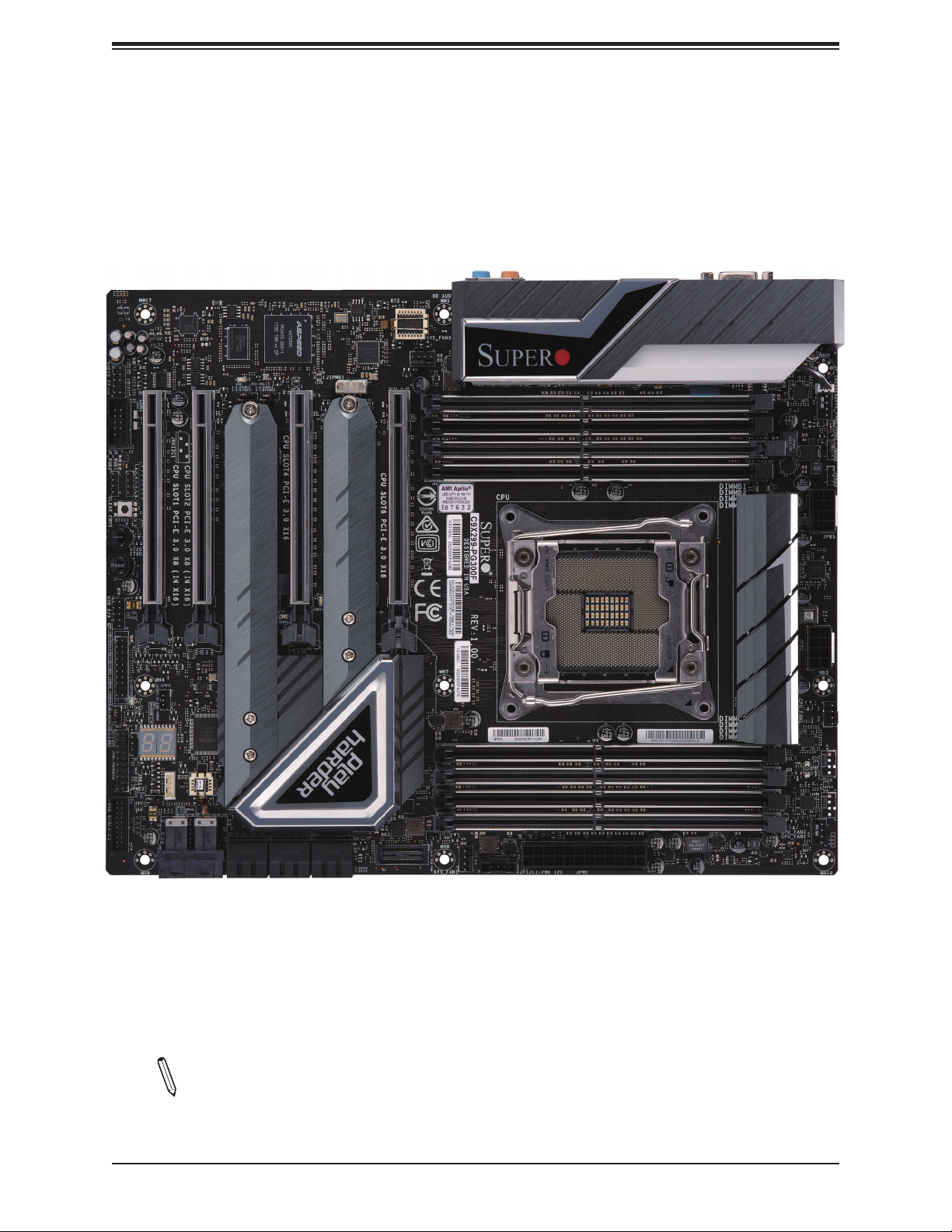
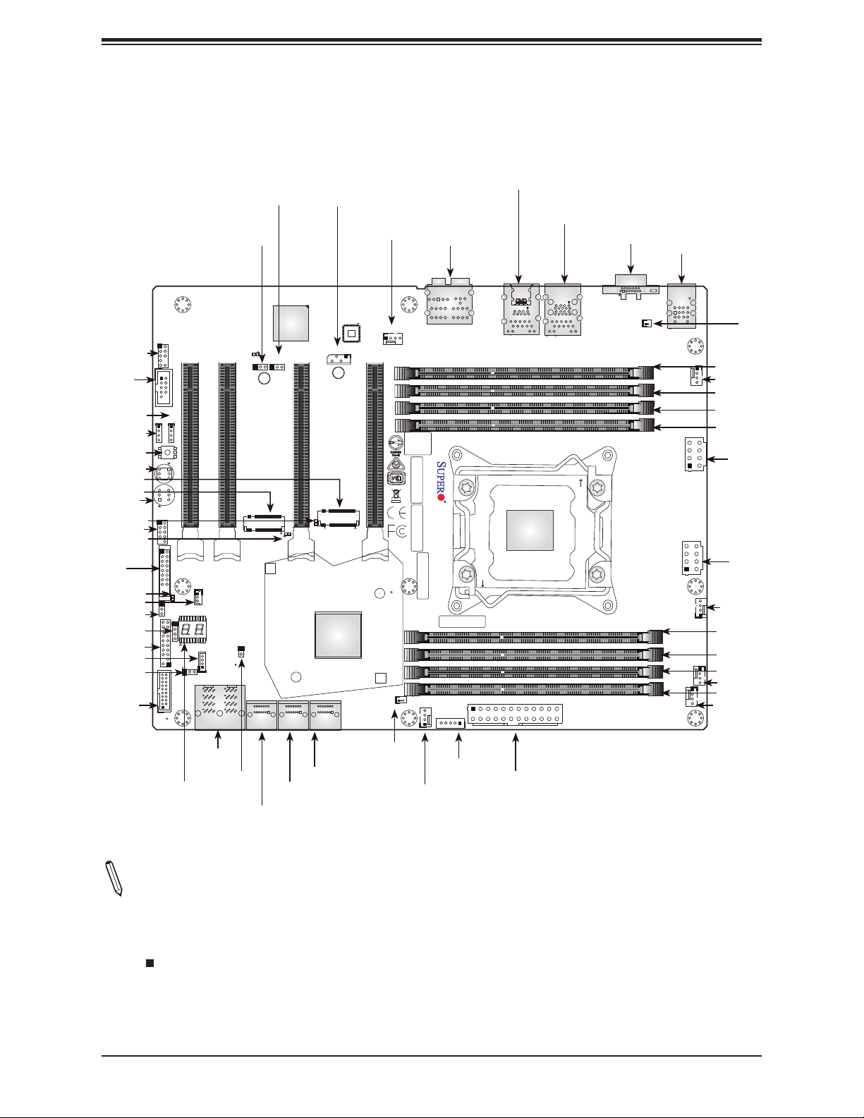
Figure 1-1. C9X299-PG300F Motherboard Image
Note: All graphics shown in this manual were based upon the latest PCB revision
available at the time of publication of the manual. The motherboard you received may
or may not look exactly the same as the graphics shown in this manual.
8
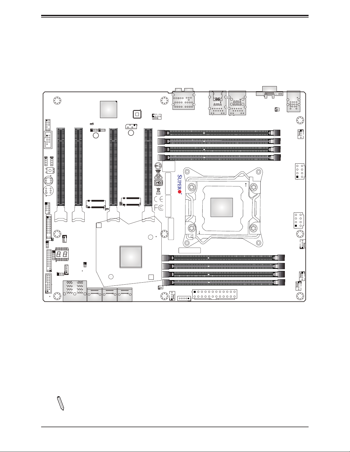
Chapter 1: Introduction
JP_RGB2
CLEAR CMOS
AUDIO_FP
COM1
JP_RGB1
CPU SLOT1 PCI-E 3.0 X8 (IN X16)
Power
Button
Reset
Button
USB 2/3
Figure 1-2. C9X299-PG300F Motherboard Layout
A C
JPG1:VGA
JPB1
CPU SLOT2 PCI-E 3.0 X8 (IN X16)
PCI-E M.2-M1
C
LED6904
BMC
JIPMB1
CPU SLOT4 PCI-E 3.0 X16
PCI-E M.2-M2
A
C
LED6903
A
LAN CTRL
CPU SLOT6 PCI-E 3.0 X16
(not drawn to scale)
SYS_FAN3
BIOS
LICENSE
MAC CODE
BAR CODE
HD AUDIO
C9X299-PG300F REV:1.01
DESIGNED IN USA
MAC CODE
LAN2 LAN1
USB3.0 (3.1 Gen1) 4/5USB3.1 (3.1 Gen2) 6/7
CPU
OPEN 1st
VGA
BT1
DIMMB1
DIMMB2
DIMMA1
DIMMA2
KB/Mouse
USB 0/1
JPW2
SYS_FAN2
JPW3
JF1
LED7201
C
A
JWD1
JTPM1:TPM/PORT80
JD1
RAID KEY-1
USB3.0 (3.1 Gen1) 8/9
JPME2
JSTBY1
LED1
JRK1
U.2-1
U.2-2
JL1
I-SATA4
I-SATA5
I-SATA2
I-SATA3
I-SATA0
I-SATA1
PCH
1
JSD1:SATA DOM PWR
SYS_FAN1
JPI2C1:PWR I2C
IPMI CODE
JPW1
CLOSE 1st
CPU_FAN1
12V_PUMP_PWR1
DIMMC2
DIMMC1
DIMMD2
DIMMD1
CPU_FAN2
24
Note: Components not documented are for internal testing only.
9
Super C9X299-PG300F User's Manual
JPG1
JPB1
BMC
AUDIO_FP
COM1
JP_RGB1
JP_RGB2
CLEAR CMOS
Power Button
PCI-E M.2-M2
PCI-E M.2-M1
Reset Button
LED6903
USB 2/3
LED6904
JF1
LED7201
JSTBY1
JWD1
JD1
JTPM1
JRK1
JPME2
USB 3.0
(3.1 Gen1)
8/9
AUDIO_FP
COM1
JP_RGB1
JP_RGB2
CLEAR CMOS
Power
Button
Reset
Button
USB 2/3
JF1
LED7201
C
A
JWD1
JTPM1:TPM/PORT80
JD1
RAID KEY-1
USB3.0 (3.1 Gen1) 8/9
LED1
CPU SLOT1 PCI-E 3.0 X8 (IN X16)
JSTBY1
LED1
JRK1
JPME2
U.2-1
U.2-2
A C
JPG1:VGA
JPB1
CPU SLOT2 PCI-E 3.0 X8 (IN X16)
PCI-E M.2-M1
JL1
I-SATA4
U.2-1
I-SATA5
U.2-2
I-SATA2~3
I-SATA4~5
CPU SLOT4 PCI-E 3.0 X16
A
C
LED6904
I-SATA2
I-SATA3
I-SATA0~1
JIPMB1
PCI-E M.2-M2
A
C
LED6903
I-SATA0
I-SATA1
Quick Reference
LAN2
USB 3.1 (3.1 Gen2) 6/7
SYS_FAN3
LAN CTRL
JIPMB1
CPU SLOT6 PCI-E 3.0 X16
PCH
JSD1:SATA DOM PWR
HD AUDIO
SYS_FAN3
BIOS
LICENSE
MAC CODE
DESIGNED IN USA
BAR CODE
MAC CODE
1
SYS_FAN1
JSD1
SYS_FAN1
HD AUDIO
C9X299-PG300F REV:1.01
JPI2C1:PWR I2C
IPMI CODE
JPI2C1
JPW1
CLOSE 1st
JPW1JL1
LAN1
USB 3.0 (3.1 Gen1) 4/5
LAN2 LAN1
USB3.0 (3.1 Gen1) 4/5USB3.1 (3.1 Gen2) 6/7
OPEN 1st
CPU
24
VGA
VGA
BT1
DIMMB1
DIMMB2
DIMMA1
DIMMA2
KB/Mouse
USB 0/1
KB/Mouse
USB 0/1
SYS_FAN2
JPW3
JPW2
CPU_FAN1
12V_PUMP_PWR1
DIMMC2
DIMMC1
DIMMD2
DIMMD1
CPU_FAN2
BT1
DIMMB1
SYS_FAN2
DIMMB2
DIMMA1
DIMMA2
JPW3
JPW2
CPU_FAN1
DIMMC2
DIMMC1
DIMMD2
12V_PUMP_PWR1
DIMMD1
CPU_FAN2
Notes:
• See Chapter 2 for detailed information on jumpers, I/O ports, and JF1 front panel connec-
tions. Jumpers/LED indicators not indicated are used for testing only.
• " " indicates the location of Pin 1.
• When LED7201 (Onboard Power LED indicator) is on, system power is on. Unplug the
power cable before installing or removing any components.
10

Chapter 1: Introduction
Quick Reference Table
Jumper Description Default Setting
CLEAR CMOS CMOS Clear Switch Push Button Switch
JPB1 IPMI Function
JPG1 VGA Enable/Disable Pins 1-2 (Enable)
JPME2 Intel Manufacturing Mode Pins 1-2 (Normal)
JWD1 Watch Dog Function Enable Pins 1-2 (RST)
POWER BUTTON Internal Power Button Push Button Switch
RESET BUTTON Onboard System Reset Button Push Button Switch
LED Description Status
LED1 Status Code LED Digital Readout
LED6903 M.2 Connector 2 SSD Active LED Activity: Green Blinking
LED6904 M.2 Connector 1 SSD Active LED Activity: Green Blinking
LED7201 Onboard Standby PWR LED Power On: Green On
Pins 1-2 (Enabled)
Pins 2-3 (Disable)
Connector Description
12V_PUMP_PWR1 12V 4-pin power connector for CPU liquid cooling pump
AUDIO_FP Front Panel Audio Header
BT1 Onboard Battery Header
COM1 COM1 Header
CPU_FAN1, CPU_FAN2 CPU Fan Headers
CPU SLOT 1/2 PCI-E 3.0 x8 (IN x16) PCI-E x16 Slots (PCI-E 3.0 x8 link)
CPU SLOT 4/6 PCI-E 3.0 x16 PCI-E x16 Slots (PCI-E 3.0 x16 link)
HD AUDIO High Denition Audio Header
I-SATA0~5 (Intel X299) Serial ATA (SATA 3.0) Ports 0~5 (6Gb/sec)
JD1 Speaker Header (Pins 1-4: Speaker)
JF1 Front Control Panel Header
JIPMB1 4-pin External I2C Header (for an IPMI card)
JL1 Chassis Intrusion Header
JPI2C1 Power Supply SMBus I2C Header
JP_RGB1, JP_RGB2 LED Light Bar Headers
JPW1 24-pin ATX Main Power Connector (Required)
JPW2, JPW3 +12V 8-pin CPU Power Connectors (Required)
JRK1 Intel RAID Key Header
JSD1 SATA Disk-On-Module (DOM) Power Connector
JSTBY1 Standby Power Header
Note: The table above is continued on the next page.
11

Super C9X299-PG300F User's Manual
Connector Description
JTPM1 Trusted Platform Module (TPM)/Port 80 Header
KB/MOUSE PS/2 Keyboard/Mouse Port
LAN1, LAN2 LAN1: 10Gb LAN Port, LAN2: 1Gb LAN Port
PCI-E M.2-M1, PCI-E M.2-M2 PCI-E M.2 Connectors 1 and 2 (Small form factor devices and other portable devices
for high speed SSDs)
SYS_FAN1/2/3 System Fan Headers
U.2-1, U.2-2 U.2 Connector 1 and 2 for 2.5" NVME SSD Drives
USB 0/1 Back Panel USB 2.0 Ports
USB 2/3 Front Access USB 2.0 Header
USB 4/5 Back Panel USB 3.1 Gen1 Ports
USB 6/7 Back Panel USB 3.1 Gen2 Ports (USB6: Type A, USB7: Type C)
USB 8/9 Front Panel USB 3.1 Gen1 Header
12
Chapter 1: Introduction
Motherboard Features
Motherboard Features
CPU
•
The C9X299-PG300F motherboard supports a single Intel Core X-Series processor in an LGA2066 socket.
Memory
•
Supports up to 128GB of unbuffered Non-ECC DDR4 memory, two DIMMs per channel (2DPC) with speeds of up to
2400MHz~4000MHz (overclocked)
DIMM Size
• 4GB, 8GB, 16GB at 1.2V
Note 1: Memory speed support depends on the processor used in the system.
Note 2: For the latest CPU/memory updates, please refer to our website at http://www.supermicro.com/products/
motherboard.
Chipset
•
Intel PCH X299
Expansion Slots
•
Four (4) PCI-E 3.0 x16 slots
• Two (2) M.2 PCI-E 3.0 x4 slots (2280 x2)
• Two (2) U.2 slots
Network
•
Intel I210AT
• Aquantia AQC 107
Audio
•
Realtek ALC1220 - HD Audio 7.1
• One (1) Front Panel Audio Header
• One (1) S/PDIF Out on the rear side of the chassis
I/O Devices
Serial (COM) Header • One (1) front accessible serial header (COM1)
•
• SATA 3.0 • Six (6) I-SATA 3.0 ports (I-SATA0 ~ 5)
• RAID PCH • RAID 0, 1, 5, and 10
Peripheral Devices
• One (1) USB 3.1 Gen2 Type C port on the I/O back panel
• One (1) USB 3.1 Gen2 Type A port on the I/O back panel
• Two (2) USB 3.1 Gen1 ports on the I/O back panel
• Two (2) front accessible USB 3.1 Gen1 connections via one header
• Two (2) USB 2.0 ports on the I/O back panel
• Two (2) front accessible USB 2.0 connections via one header
Note: The table above is continued on the next page.
13
Super C9X299-PG300F User's Manual
Motherboard Features
BIOS
•
128Mb AMI BIOS® SPI Flash BIOS
• PCI-E 3.0, ACPI 3.0, BIOS rescue hot-key, Overclock support
Power Management
•
ACPI power management
• Power button override mechanism
• Power-on mode for AC power recovery
System Health Monitoring
•
Onboard voltage monitors for CPU cores, +3.3V, +5V, +/-12V, +3.3V Stby, +5V Stby, VBAT, Memory, PCH temperature,
System temperature, and Memory temperature
• CPU 8 phase-switching voltage regulator
• CPU/System overheat control
• CPU Thermal Trip support
Fan Control
•
Five (5) proprietary 4-pin fan headers
• Fan status monitoring via IPMI connections
• Dual cooling zone
• Multi-speed fan control via onboard BMC
• Pulse Width Modulation (PWM) fan control
System Management
•
PECI (Platform Environment Control Interface) 3.1 support
• SuperDoctor® 5, Watch Dog, NMI
• Chassis Intrusion header and detection
• Power supply monitoring
LED Indicators
CPU/System overheat LED
•
• Power LED
• Fan failed LED
• HDD activity LED
• LAN activity LED
Other
•
RoHS
Dimensions
•
ATX form factor (12.0" x 9.6") (304.80 mm x 243.84 mm)
Note 1: The CPU maximum thermal design power (TDP) is subject to chassis and
heatsink cooling restrictions. For proper thermal management, please check the chas-
sis and heatsink specications for proper CPU TDP sizing.
14
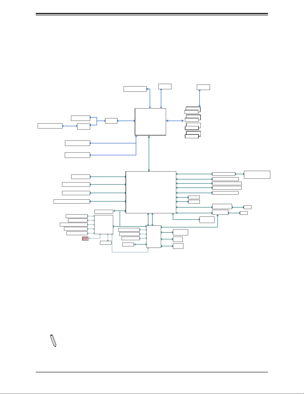
Figure 1-3.
Chipset Block Diagram (28 Lanes)
Chapter 1: Introduction
PCI-E x16 SLOT2
USB3.1 Type A+Type C
PCI-E 3.0 x4
SWITCH
PCI-E x16 SLOT4
PCI-E x16 SLOT6
6X SATA-III
M.2 SOCKET SSD
M.2 SOCKET SSD
COM1 Header
PS2 KB/MS
FAN SPEED CTRL
Voltage monitor
Temp Sensor
SWITCH
PCI-E 3.0 x16
SATA-III
6Gb/s
PCI-E 3.0 x4
8GT/s
PCI-E 3.0 x4
8GT/s
PCI-E 3.0 x2
8GT/s
TPM Header
NCT6792D-B
LPC I/O
SMBUS
PCH
PCI-E 3.0 x8
8.0GT/s
8.0GT/s
SKX-X : VR13
PCI-E 3.0 x4
8.0GT/s
LPC
FAN SPEED CTRL
Voltage monitor
Te
mp Sensor
SMBUS
SVID
Intel
PCI-E-28 Lanes
(Socket-R)
x4 DMI
8GT/s
Intel
PCH
USB 2.0 x2
PCI-E 3.0 x1
AST2500
SMBUS
SMBUS
RMII
DDR4 (2DPC)
Non-ECC UDIMM
DIMMA1
DIMMB1
DIMMC1
DIMMD1
AZALIA
USB3.0
5Gbps
USB2.0
480Mbps
PCI-E 3.0 x2
PCI-E 3.0 x1
FLASH
SPI 128Mb
VGA
DDR4
DIMMA0
DIMMB0
DIMMC0
DIMMD0
USB3.0
5Gbps
USB2.0
480Mbps
GPIO
SMBUS
8GT/s
8GT/s
SMBUS
FLASH
SPI 128Mb
Realtek ALC1220
2 X USB 3.0 Rear
2 X USB 3.0 Header
2 X USB 2.0 Header
2 X USB 2.0 Rear
GLAN
AQC107-B1-C
GLAN
WGI210AT
Share LAN
Audio Jack/
Audio Pin Header
RJ45
RJ45
Note: This is a general block diagram and may not exactly represent the features on
your motherboard. See the previous pages for the actual specications of your motherboard.
15

Super C9X299-PG300F User's Manual
Chipset Block Diagram (44 Lanes)
Figure 1-3.
PCI-E x16 SLOT2
USB3.1 Type A+Type C
PCI-E x16 SLOT1
PCI-E 3.0 x4
PCI-E 3.0 x4
PCI-E 3.0 x8
SWITCH
PCI-E x16 SLOT4
PCI-E x16 SLOT6
6X SATA-III
M.2 SOCKET SSD
M.2 SOCKET SSD
COM1 Header
PS2 KB/MS
FAN SPEED CTRL
Voltage monitor
Temp Sensor
PCI-E 3.0 x8
PCI-E 3.0 x4
PCI-E 3.0 x8
TPM Header
NCT6792D-B
SWITCH
SWITCH
SWITCH
PCI-E 3.0 x8
8.0GT/s
PCI-E 3.0 x8
8.0GT/s
SATA-III
6Gb/s
PCI-E 3.0 x4
8GT/s
PCI-E 3.0 x4
8GT/s
PCI-E 3.0 x2
8GT/s
LPC I/O
SMBUS
PCH
SKX-X : VR13
PCI-E 3.0 x8
8.0GT/s
PCI-E 3.0 x4
8.0GT/s
PCI-E 3.0 x8
8.0GT/s
LPC
FAN SPEED CTRL
Voltage monitor
Temp Sensor
SMBUS
SVID
Intel
PCI-E-44 Lanes
(Socket-R)
x4 DMI
8GT/s
Intel
PCH
USB2.0 x2
PCI-E 3.0 x1
AST2500
SMBUS
SMBUS
RMII
DDR4 (2DPC)
Non-ECC UDIMM
DIMMA0
DIMMA1
DIMMB0
DIMMB1
DIMMC0
DIMMC1
DIMMD0
DIMMD1
AZALIA
USB3.0
5Gbps
USB2.0
480Mbps
PCI-E 3.0 x1
8GT/s
FLASH
SPI 128Mb
VGA
DDR4
USB3.0
USB2.0
480Mbps
GPIO
SMBUS
SMBUS
5Gbps
PCI-E 3.0 x2
8GT/s
FLASH
SPI
128Mb
Realtek ALC1220
2 X USB 3.0 Rear
2 X USB 3.0 Header
2 X USB 2.0 Header
2 X USB 2.0 Rear
GLAN
AQC107-B1-C
GLAN
WGI210AT
Audio Jack/
Audio Pin Header
RJ45
RJ45
Note: This is a general block diagram and may not exactly represent the features on
your motherboard. See the previous pages for the actual specications of your motherboard.
16

Chapter 1: Introduction
1.2 Processor and Chipset Overview
The C9X299-PG300F supports an Intel Core X-Series processor in the LGA2066 socket. With
the Intel X299 PCH, the C9X299-PG300F is a high-end, multi-GPU motherboard that offers
reliability and stability. It offers the latest high-performance features such as NVMe, M.2/U.2
storage interfaces, and DDR4 memory with speeds of up to 4000MHz (OC).
The C9X299-PG300F supports the following features:
• ACPI Power Management Logic Support Rev. 4.0a
• Intel Turbo Boost Technology
• Congurable TDP (cTDP) and Lower-Power Mode
• Adaptive Thermal Management/Monitoring
• PCI-E 3.0, SATA 3.0, NVMe, U.2 and M.2 connectors
• System Management Bus (SMBus) Specication Version 2.0
• Intel Trusted Execution Technology (Intel TXT)
• Intel Rapid Storage Technology
• Intel Virtualization Technology for Directed I/O (Intel VT-d)
1.3 Special Features
This section describes the health monitoring features of the C9X299-PG300F motherboard.
The motherboard has an onboard System Hardware Monitor chip that supports system health
monitoring.
Recovery from AC Power Loss
The Basic I/O System (BIOS) provides a setting that determines how the system will respond
when AC power is lost and then restored to the system. You can choose for the system to
remain powered off (in which case you must press the power switch to turn it back on), or
for it to automatically return to the power-on state. See the Advanced BIOS Setup section
for this setting. The default setting is Last State.
17

Super C9X299-PG300F User's Manual
1.4 System Health Monitoring
The motherboard has an onboard Baseboard Management Controller (BMC) chip that
supports system health monitoring.
Onboard Voltage Monitors
The onboard voltage monitor will continuously scan crucial voltage levels. Once a voltage
becomes unstable, it will give a warning or send an error message to the screen. Users can
adjust the voltage thresholds to dene the sensitivity of the voltage monitor. Real time readings
of these voltage levels are all displayed in the BIOS.
Fan Status Monitor with Firmware Control
The system health monitor embedded in the BMC chip can check the RPM status of the
cooling fans. The CPU and chassis fans are controlled via IPMI.
Environmental Temperature Control
System Health sensors in the BMC monitor the temperatures and voltage settings of onboard
processors and the system in real time via the IPMI interface. Whenever the temperature of
the CPU or the system exceeds a user-dened threshold, system/CPU cooling fans will be
turned on to prevent the CPU or the system from overheating
Note: To avoid possible system overheating, please be sure to provide adequate air-
ow to your system.
System Resource Alert
This feature is available when used with SuperDoctor 5 in the Windows OS or in the Linux
environment. SuperDoctor is used to notify the user of certain system events. For example,
you can congure SuperDoctor to provide you with warnings when the system temperature,
CPU temperatures, voltages, and fan speeds go beyond a predened range.
1.5 ACPI Features
ACPI stands for Advanced Conguration and Power Interface. The ACPI specication denes
a exible and abstract hardware interface that provides a standard way to integrate power
management features throughout a computer system, including its hardware, operating
system, and application software. This enables the system to automatically turn on and off
peripherals such as CD-ROMs, network cards, hard disk drives, and printers.
18
Chapter 1: Introduction
In addition to enabling operating system-directed power management, ACPI also provides a
generic system event mechanism for Plug and Play, and an operating system-independent
interface for conguration control. ACPI leverages the Plug and Play BIOS data structures,
while providing a processor architecture-independent implementation that is compatible with
Windows® 7, Windows 8, and Windows 2012 Operating Systems.
1.6 Power Supply
As with all computer products, a stable power source is necessary for proper and reliable
operation. It is even more important for processors that have high CPU clock rates.
The C9X299-PG300F motherboard accommodates a 24-pin ATX power supply. Although most
power supplies generally meet the specications required by the CPU, some are inadequate.
In addition, a 12V 8-pin power connection is also required to ensure adequate power supply
to the system.
Warning: To prevent damage to the power supply or the motherboard, use power
supplies that contain 24-pin and 8-pin power connectors. Connect the power supplies
to the 24-pin (JPW1) and the 8-pin power connectors (JPW2/JPW3) on the motherboard. Failure in doing so may void the manufacturer warranty on your power supply
and motherboard.
It is strongly recommended that you use a high quality power supply that meets ATX power
supply Specication 2.02 or above. It must also be SSI compliant. For more information,
please refer to the website at http://www.ssiforum.org/. Additionally, in areas where noisy
power transmission is present, you may choose to install a line lter to shield the computer
from noises. It is recommended that you also install a power surge protector to help avoid
problems caused by power surges.
1.7 Serial Port
The C9X299-PG300F motherboard supports one serial communication connection. COM1
header can be used for input/output. The UART provides legacy speeds with a baud rate of
up to 115.2 Kbps as well as an advanced speed with baud rates of 250 K, 500 K, or 1 Mb/s,
which support high-speed serial communication devices.
19

Super C9X299-PG300F User's Manual
Chapter 2
Installation
2.1 Static-Sensitive Devices
Electrostatic Discharge (ESD) can damage electronic com ponents. To prevent damage to your
motherboard, it is important to handle it very carefully. The following measures are generally
sufcient to protect your equipment from ESD.
Precautions
• Use a grounded wrist strap designed to prevent static discharge.
• Touch a grounded metal object before removing the board from the antistatic bag.
• Handle the board by its edges only; do not touch its components, peripheral chips, memory
modules or gold contacts.
• When handling chips or modules, avoid touching their pins.
• Put the motherboard and peripherals back into their antistatic bags when not in use.
• For grounding purposes, make sure your computer chassis provides excellent conductivity
between the power supply, the case, the mounting fasteners, and the motherboard.
• Use only the correct type of onboard CMOS battery. Do not install the onboard battery
upside down to avoid possible explosion.
Unpacking
The motherboard is shipped in antistatic packaging to avoid static damage. When unpacking
the motherboard, make sure that the person handling it is static protected.
20
Chapter 2: Installation
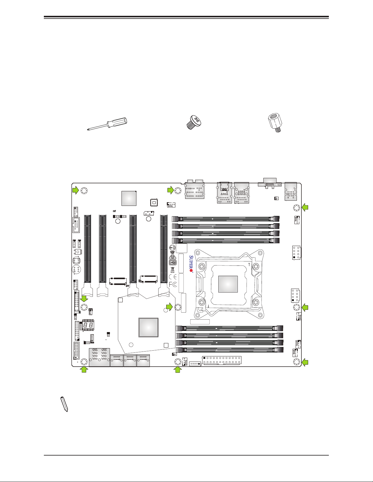
2.2 Motherboard Installation
All motherboards have standard mounting holes to t different types of chassis. Make sure
that the locations of all the mounting holes for both the motherboard and the chassis match.
Although a chassis may have both plastic and metal mounting fasteners, metal ones are
highly recommended because they ground the motherboard to the chassis. Make sure that
the metal standoffs click in or are screwed in tightly.
Phillips Screwdriver (1)
Tools Needed
AUDIO_FP
COM1
JP_RGB1
JP_RGB2
CLEAR CMOS
Button
Button
USB 2/3
JF1
LED7201
C
A
JWD1
JTPM1:TPM/PORT80
JD1
RAID KEY-1
USB3.0 (3.1 Gen1) 8/9
CPU SLOT1 PCI-E 3.0 X8 (IN X16)
Power
Reset
JSTBY1
LED1
JPME2
A C
JPG1:VGA
JPB1
CPU SLOT2 PCI-E 3.0 X8 (IN X16)
PCI-E M.2-M1
JL1
JRK1
I-SATA4
U.2-1
I-SATA5
U.2-2
C
LED6904
BMC
JIPMB1
CPU SLOT4 PCI-E 3.0 X16
PCI-E M.2-M2
A
C
LED6903
A
PCH
I-SATA0
I-SATA2
I-SATA1
I-SATA3
Phillips Screws (9)
LAN CTRL
SYS_FAN3
CPU SLOT6 PCI-E 3.0 X16
BIOS
LICENSE
C9X299-PG300F REV:1.01
MAC CODE
DESIGNED IN USA
BAR CODE
MAC CODE
1
JSD1:SATA DOM PWR
SYS_FAN1
JPI2C1:PWR I2C
HD AUDIO
IPMI CODE
JPW1
CLOSE 1st
LAN2 LAN1
USB3.0 (3.1 Gen1) 4/5USB3.1 (3.1 Gen2) 6/7
CPU
Standoffs (9)
Only if Needed
VGA
OPEN 1st
24
BT1
DIMMB1
DIMMB2
DIMMA1
DIMMA2
DIMMC2
DIMMC1
DIMMD2
DIMMD1
KB/Mouse
USB 0/1
JPW2
CPU_FAN2
SYS_FAN2
JPW3
CPU_FAN1
12V_PUMP_PWR1
Location of Mounting Holes
Notes: 1. To avoid damaging the motherboard and its components, please do not use
a force greater than 8 lb/inch on each mounting screw during motherboard installation.
2. Some components are very close to the mounting holes. Please take precautionary
measures to avoid damaging these components when installing the motherboard to
the chassis.
21
Super C9X299-PG300F User's Manual
Installing the Motherboard
1. Locate the mounting holes on the motherboard. See the previous page for the location.
2. Locate the matching mounting holes on the chassis. Align the mounting holes on the
motherboard against the mounting holes on the chassis.
3. Install standoffs in the chassis as needed.
4. Install the motherboard into the chassis carefully to avoid damaging other motherboard
components.
5. Using the Phillips screwdriver, insert a Phillips head #6 screw into a mounting hole on
the motherboard and its matching mounting hole on the chassis.
6. Repeat Step 5 to insert remaining screws into all mounting holes.
7. Make sure that the motherboard is securely placed in the chassis.
Note: Images displayed are for illustration only. Your chassis or components might
look different from those shown in this manual.
22

Chapter 2: Installation
2.3 Installing an M.2 Device (optional)
Two M.2 (M-key) connectors are supported by the C9X299-PG300F. M.2 devices are used
for solid state storage and internal expansion. Follow the steps below in order to install an
M.2 device.
Note: A screwdriver will be required.
1. Locate and remove the retaining screws on the M.2 heatsink.
2. With the heatsink removed, locate the appropriate standoff for the M.2 card's length.
3. Remove the associated standoff screw and set it aside.
4. Carefully plug the M.2 device into the M.2 connector and lower the semi-circle notched
end onto the standoff.
5. Replace the standoff screw and tighten it to secure the M.2 device into place. Do not
overtighten so as to avoid damaging the M.2 device.
6. Replace the M.2 heatsink and the retaining screws. Tighten the screws to secure the
heatsink into place.
23
Super C9X299-PG300F User's Manual
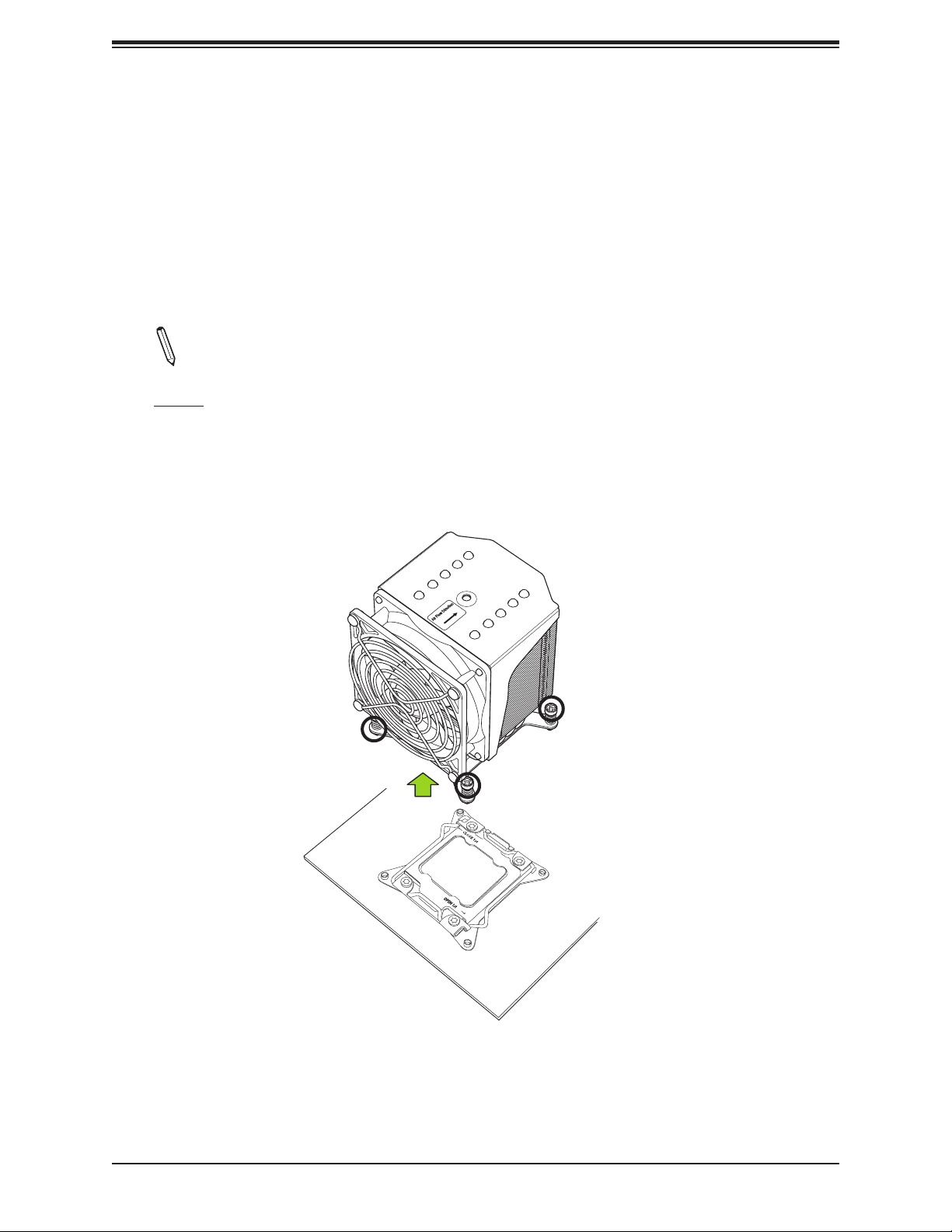
2.4 Processor and Heatsink Installation
Warning: When handling the processor package, avoid placing direct pressure on the label
area of the fan.
Important:
• Always connect the power cord last, and always remove it before adding, removing, or
changing any hardware components. Make sure that you install the processor into the CPU
socket before you install the CPU heatsink.
• If you buy a CPU separately, make sure that you use an Intel-certied multi-directional
heatsink only.
• Make sure to install the motherboard into the chassis before you install the CPU heatsink.
• When receiving a motherboard without a processor pre-installed, make sure that the plastic
CPU socket cap is in place and none of the socket pins are bent; otherwise, contact your
retailer immediately.
• Refer to the Supermicro website for updates on CPU support.
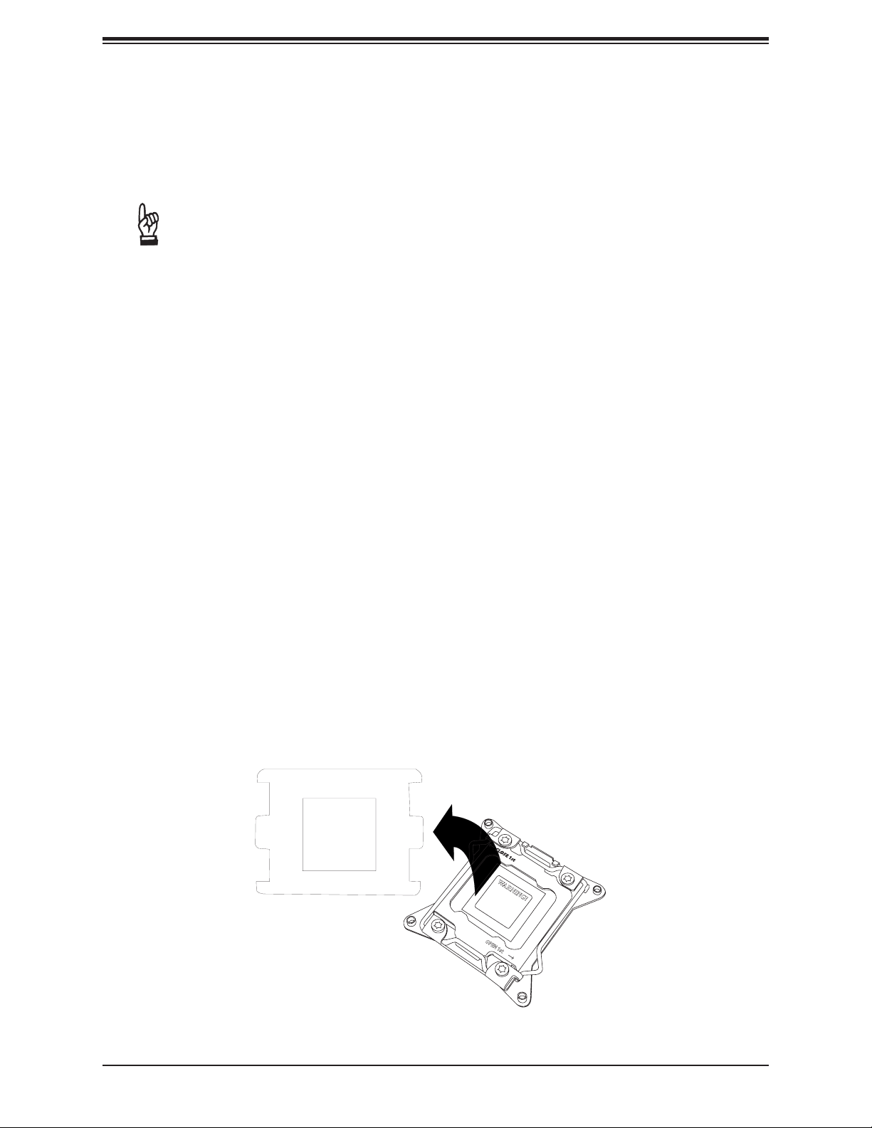
Installing a CPU
1. Remove the WARNING plastic cap from the socket.
WARNING!
24
WARNING!
OPEN 1st
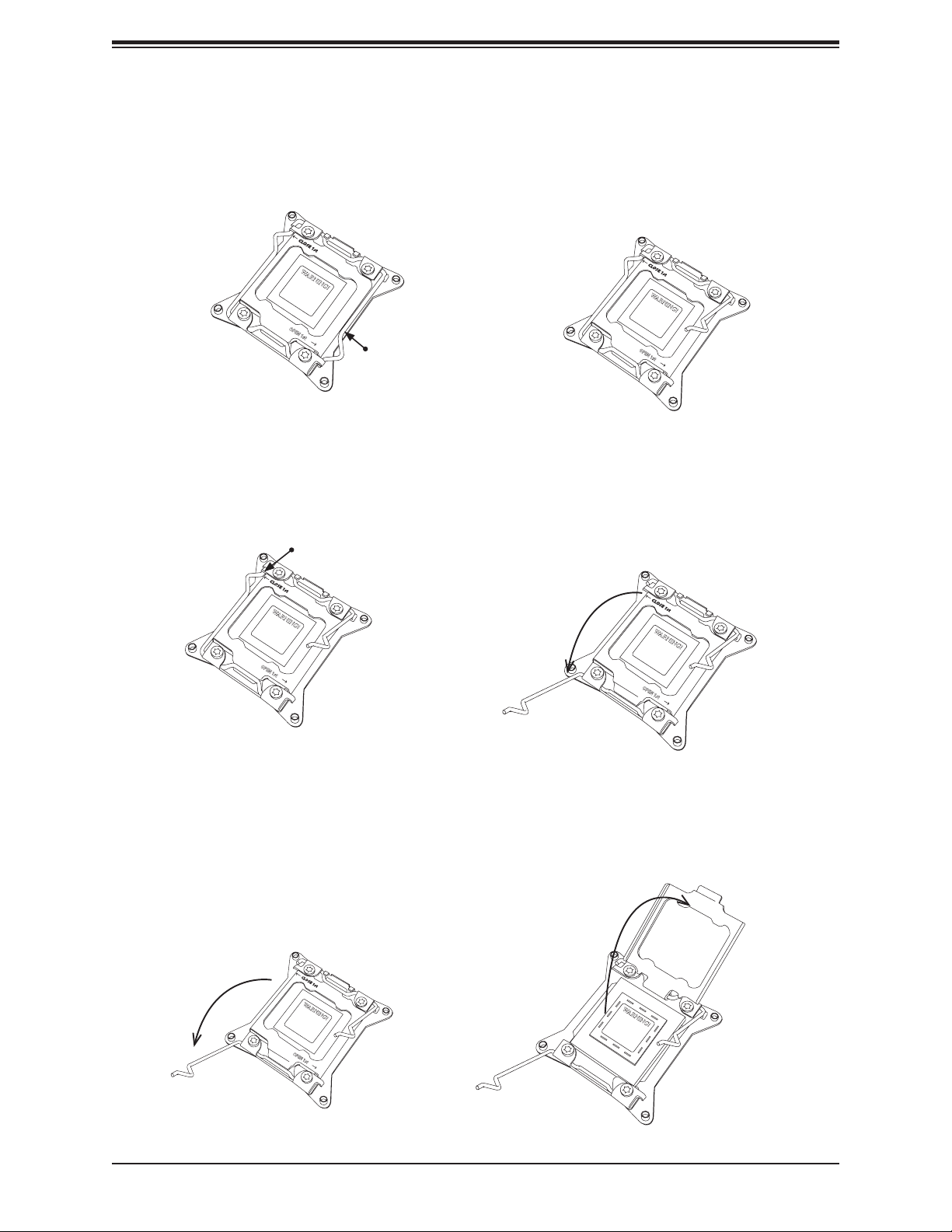
Chapter 2: Installation
2. There are two load levers on the LGA2066 socket. To open the socket cover, press and
release the "Unlock 1st" lever, marked by an unlock symbol.
1
WARNING!
OPEN 1st
Press down on
2
WARNING!
OPEN 1st
Load Lever labeled
'Open 1st'.
3. Press the "Lock 1st" lever, marked by a lock symbol, to release the load plate that
covers the CPU socket from its locking position.
Press down on
1
Lever 'Close 1st'
WARNING!
OPEN 1st
Load
Pull the lever away
2
from the socket
WARNING!
OPEN 1st
4. With the "Lock 1st" lever fully retracted, gently push down on the "Unlock 1st" lever to
open the load plate. Lift the load plate to open it completely.
Gently push down
1
to pop the load plate
open.
WARNING!
OPEN 1st
2
WARNING!
25
Super C9X299-PG300F User's Manual
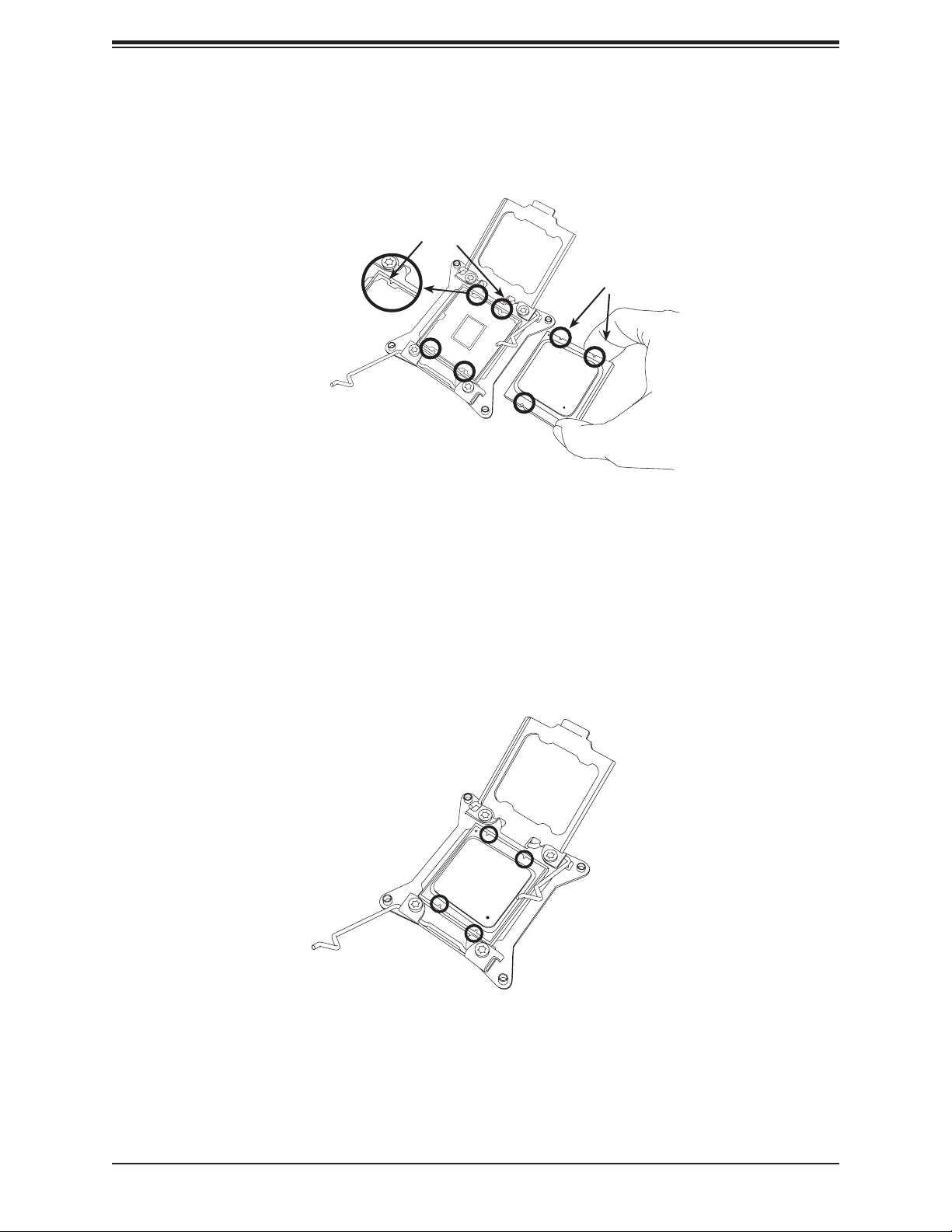
5. Use your thumb and index nger to hold the CPU on its edges. Align the CPU keys,
which have semi-circle cutouts, against the socket keys.
Socket Keys
CPU Keys
6. Once they are aligned, carefully lower the CPU straight down into the socket. To avoid
damaging the CPU or socket, do not drop the CPU onto the socket, move it horizontally
or vertically, or rub it against the socket pins.
7. With the CPU inside the socket, inspect the four corners of the CPU to make sure that it
is properly installed.
26
Chapter 2: Installation
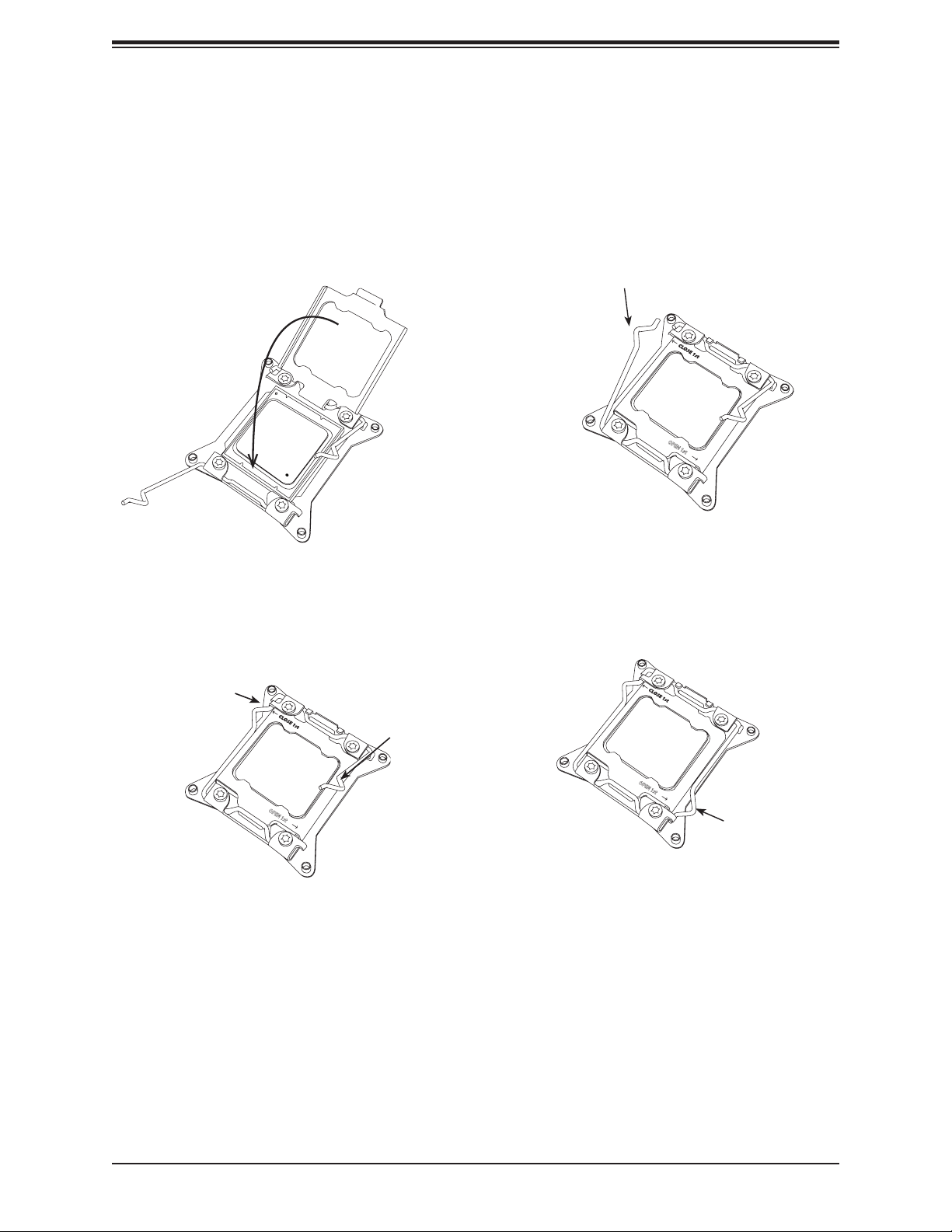
8. Close the load plate with the CPU inside the socket. Lock the "Lock 1st" lever rst, then
lock the "Unlock 1st" lever second. Gently push the load levers down to the lever locks.
Gently close the
1
3
load plate.
Lever Lock
Push down and
lock 'Open 1st'
lever
Push down and lock
2
'Close 1st' lever.
OPEN 1st
4
OPEN 1st
OPEN 1st
Lever Lock
27
Super C9X299-PG300F User's Manual
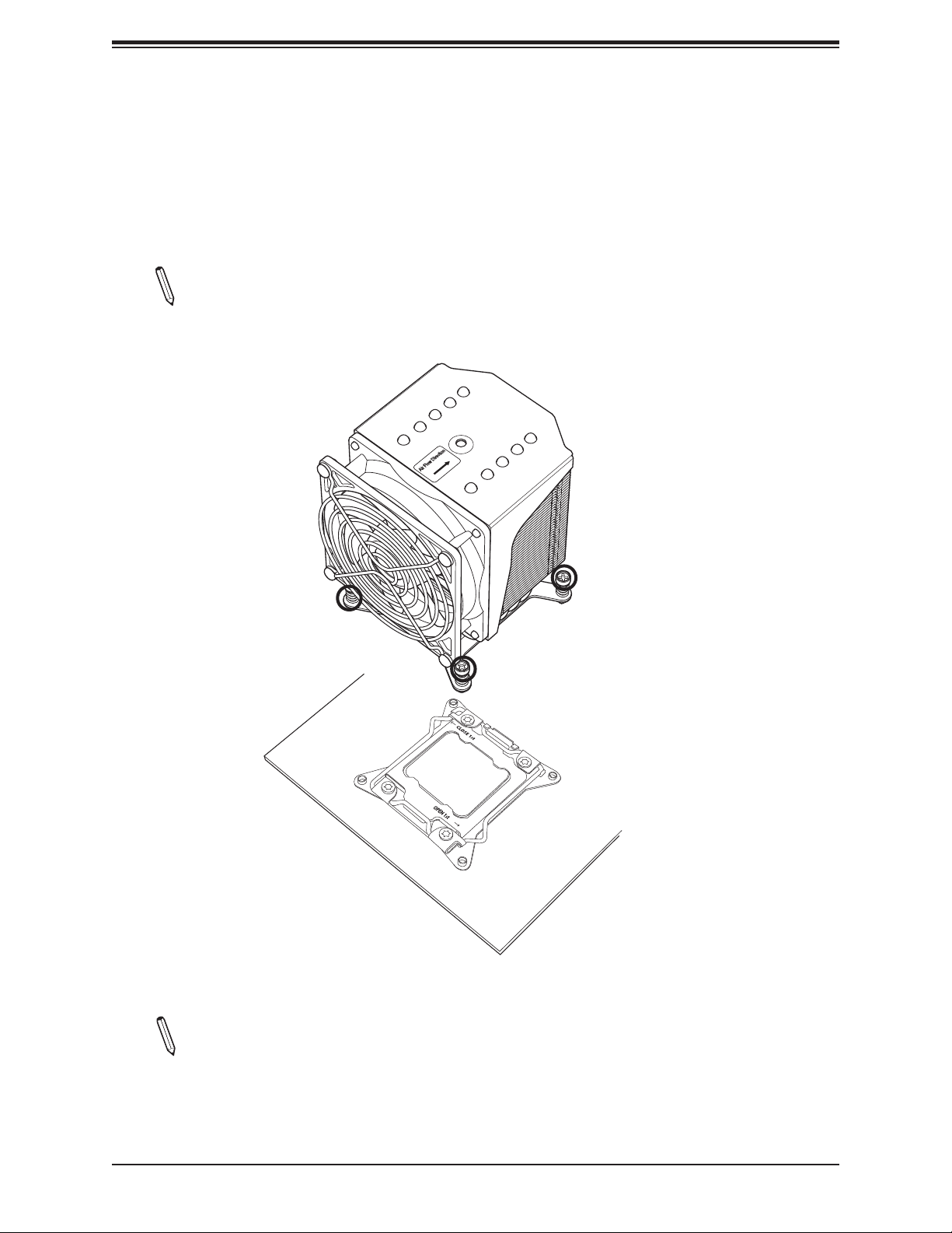
Installing a CPU Heatsink
1. Apply the proper amount of thermal grease to the heatsink.
2. Place the heatsink on top of the CPU so that the four mounting holes on the heatsink
are aligned with those on the retention mechanism. Tighten the screws in the following
order:
Note: Screw #1 is not shown in the illustration. It is found opposite of Screw #2.
Screw #3
Screw #4
Screw #2
Note: Graphic drawings included in this manual are for reference only. They might look
different from the components installed in your system.
28
Chapter 2: Installation
Removing a Heatsink
Warning: We do not recommend that the CPU or the heatsink be removed. However, if you
do need to remove the heatsink, please follow the instructions below to uninstall the heatsink
to avoid damaging the CPU or other components.
1. Unplug the power cord from the power supply.
2. Loosen the screws in the order below.
Note: Screw #1 is not shown in the illustration. It is found opposite of Screw #2.
3. Gently wiggle the heatsink to loosen it. Do not use excessive force when wiggling the
heatsink.
4. Once the heatsink is loosened, remove it from the motherboard.
Screw #4
Screw #3
Screw #2
29
Super C9X299-PG300F User's Manual
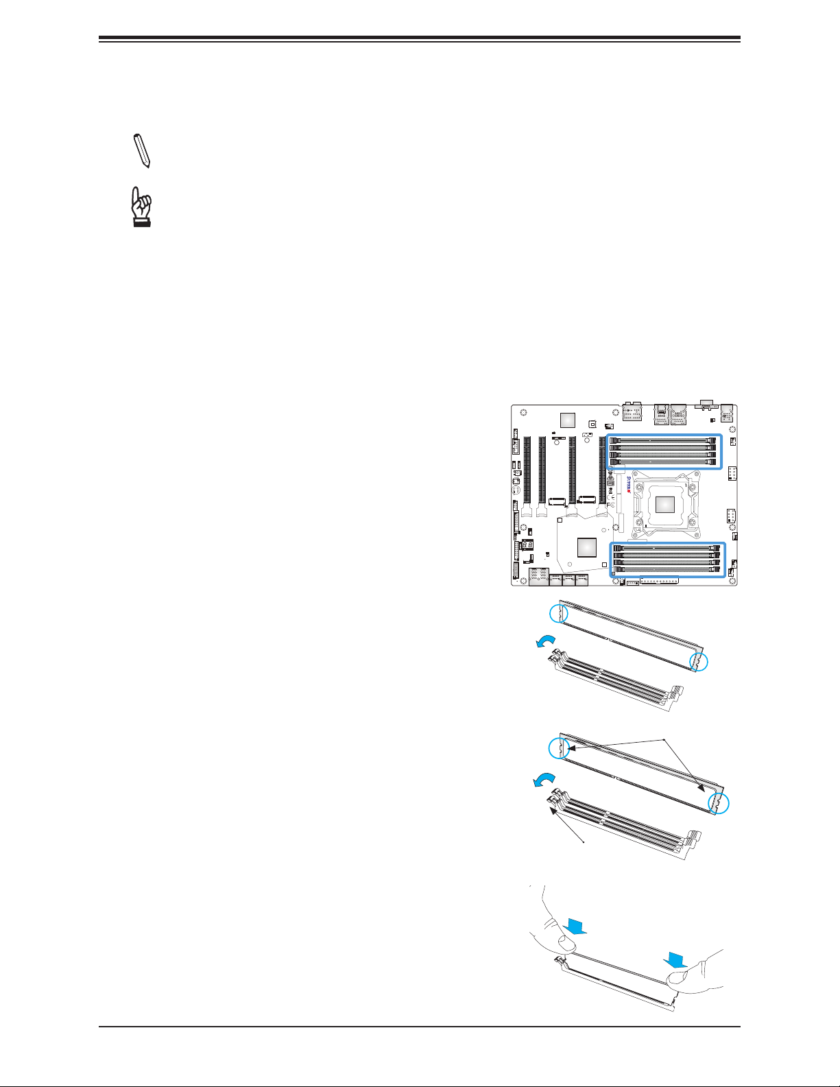
2.5 Memory Support and Installation
Note: Check the Supermicro website for recommended memory modules.
Important: Exercise extreme care when installing or removing DIMM modules to pre-
vent any possible damage.
Memory Support
The C9X299-PG300F motherboard supports up to 128GB of Non-ECC DDR4 memory with
speeds of up to 4000MHz (overclocked) in eight memory slots. Populating these DIMM slots
with memory modules of the same type and size will result in interleaved memory, which will
improve memory performance.
DIMM Installation
1. Insert the desired number of DIMMs into the
memory slots, starting with DIMMA1, DIMMB1,
DIMMC1, DIMMD1, then DIMMA2, DIMMB2,
DIMMC2, DIMMD2. For best performance,
please use the memory modules of the same
type and speed.
2. Push the release tabs outwards on both ends
of the DIMM slot to unlock it.
3. Align the key of the DIMM module with the
receptive point on the memory slot.
4. Align the notches on both ends of the module
against the receptive points on the ends of the
slot.
5. Use two thumbs together to press the notches
on both ends of the module straight down into
the slot until the module snaps into place.
JP_RGB2
CLEAR CMOS
JTPM1:TPM/PORT80
AUDIO_FP
COM1
JP_RGB1
Power
Button
Reset
Button
USB 2/3
JF1
LED7201
C
A
JWD1
JD1
RAID KEY-1
USB3.0 (3.1 Gen1) 8/9
JPME2
CPU SLOT2 PCI-E 3.0 X8 (IN X16)
CPU SLOT1 PCI-E 3.0 X8 (IN X16)
JSTBY1
LED1
JRK1
U.2-1
U.2-2
JPB1
PCI-E M.2-M1
JL1
VGA
LAN CTRL
BMC
SYS_FAN3
HD AUDIO
LAN2 LAN1
JIPMB1
A C
JPG1:VGA
CPU SLOT4 PCI-E 3.0 X16
CPU SLOT6 PCI-E 3.0 X16
BIOS
LICENSE
C9X299-PG300F REV:1.01
MAC CODE
PCI-E M.2-M2
A
C
LED6903
A
C
LED6904
I-SATA0
I-SATA4
I-SATA2
I-SATA5
I-SATA1
I-SATA3
DESIGNED IN USA
BAR CODE
MAC CODE
PCH
1
SYS_FAN1
JSD1:SATA DOM PWR
JPI2C1:PWR I2C
USB3.0 (3.1 Gen1) 4/5USB3.1 (3.1 Gen2) 6/7
CPU
CLOSE 1st
IPMI CODE
JPW1
BT1
KB/Mouse
USB 0/1
SYS_FAN2
DIMMB1
DIMMB2
DIMMA1
DIMMA2
JPW3
OPEN 1st
JPW2
CPU_FAN1
12V_PUMP_PWR1
DIMMC2
DIMMC1
DIMMD2
DIMMD1
CPU_FAN2
24
Notches
6. Press the release tabs to the lock positions to
secure the DIMM module into the slot.
DIMM Removal
Press both release tabs on the ends of the DIMM
module to unlock it. Once the DIMM module is
loosened, remove it from the memory slot.
30
Release Tab
Press down on the
stationary end rst,
then the locking end.
 Loading...