

Supermicro PDSMA User Manual

PDSMA
USER’S MANUAL
Revision 1.0c

The information in this User’s Manual has been carefully reviewed and is believed to be accurate.
The vendor assumes no responsibility for any inaccuracies that may be contained in this document,
makes no commitment to update or to keep current the information in this manual, or to notify any
person or organization of the updates. Please Note: For the most up-to-date version of this
manual, please see our web site at www.supermicro.com.
SUPER MICRO COMPUTER reserves the right to make changes to the product described in this
manual at any time and without notice. This product, including software, if any, and documentation may not, in whole or in part, be copied, photocopied, reproduced, translated or reduced to any
medium or machine without prior written consent.
IN NO EVENT WILL SUPER MICRO COMPUTER BE LIABLE FOR DIRECT, INDIRECT, SPECIAL,
INCIDENTAL, SPECULATIVE OR CONSEQUENTIAL DAMAGES ARISING FROM THE USE
OR INABILITY TO USE THIS PRODUCT OR DOCUMENTATION, EVEN IF ADVISED OF THE
POSSIBILITY OF SUCH DAMAGES. IN PARTICULAR, SUPER MICRO COMPUTER SHALL NOT
HAVE LIABILITY FOR ANY HARDWARE, SOFTWARE, OR DATA STORED OR USED WITH THE
PRODUCT, INCLUDING THE COSTS OF REPAIRING, REPLACING, INTEGRATING, INSTALLING
OR RECOVERING SUCH HARDWARE, SOFTWARE, OR DATA.
Any disputes arising between manufacturer and customer shall be governed by the laws of Santa
Clara County in the State of California, USA. The State of California, County of Santa Clara shall
be the exclusive venue for the resolution of any such disputes. Super Micro's total liability for
all claims will not exceed the price paid for the hardware product.
FCC Statement: This equipment has been tested and found to comply with the limits for a Class
A digital device pursuant to Part 15 of the FCC Rules. These limits are designed to provide
reasonable protection against harmful interference when the equipment is operated in a commercial
environment. This equipment generates, uses, and can radiate radio frequency energy and, if not
installed and used in accordance with the manufacturer’s instruction manual, may cause harmful
interference with radio communications. Operation of this equipment in a residential area is likely
to cause harmful interference, in which case you will be required to correct the interference at your
own expense.
California Best Management Practices Regulations for Perchlorate Materials: This Perchlorate
warning applies only to products containing CR (Manganese Dioxide) Lithium coin cells. “Perchlorate
Material-special handling may apply. See www.dtsc.ca.gov/hazardouswaste/perchlorate”
WARNING: Handling of lead solder materials used in this
product may expose you to lead, a chemical known to
the State of California to cause birth defects and other
reproductive harm.
Manual Revision 1.0c
Release Date: June 6, 2007
Unless you request and receive written permission from SUPER MICRO COMPUTER, you may not
copy any part of this document.
Information in this document is subject to change without notice. Other products and companies
referred to herein are trademarks or registered trademarks of their respective companies or mark
holders.
Copyright © 2007 by SUPER MICRO COMPUTER INC.
All rights reserved.
Printed in the United States of America

Preface
Preface
About This Manual
This manual is written for system integrators, PC technicians and
knowledgeable PC users. It provides information for the installation and use of the
PDSMA motherboard. The PDSMA supports single Intel Pentium D (Dual-
Core)/Pentium 4 Extreme Edition/Pentium 4/Celeron D LGA (Land Grid Array) 775
Processors at system bus speeds of 1066 MHz/800 MHz/533 MHz. The LGA 775
Pentium D/Pentium 4/Celeron D Processor is housed in a Flip-Chip Land Grid Array
(FC-LGA4) package that interfaces with the motherboard via an LGA775 socket.
The PDSMA supports the Intel Hyper-Threading (HT) Technology, the EM64T Tech-
nology, the Enhanced Intel SpeedStep Technology (EIST) and the Matrix Storage
Technology. Please refer to the motherboard specifi cations pages on our web site
(http://www.supermicro.com/Product) for updates or visit Intel's web site for proces-
sor support. This product is intended to be professionally installed.
Manual Organization
Chapter 1 describes the features, specifi cations and performance of the PDSMA
mainboard and provides detailed information about the chipset.
Chapter 2 provides hardware installation instructions. Read this chapter when
installing the processor, memory modules and other hardware components into the
system. If you encounter any problems, see Chapter 3, which describes trouble-
shooting procedures for the video, the memory and the system setup.
Chapter 4 includes an introduction to BIOS and provides detailed information on
running the CMOS Setup utility.
Appendix A provides BIOS POST Messages.
Appendix B lists BIOS POST Codes.
Appendix C lists Software Installation Instructions.
Conventions Used in this Manual
Special attention should be given to the following symbols for proper installation and
to prevent damage done to the components or injury to yourself:
Danger/Caution: Instructions to be strictly followed to prevent catastrophic
system failure or to avoid bodily injury.
Warning: Important information given to ensure proper system installation or
to prevent damage to the components.
Note: Additional Information given to differentiate various models and to ensure
correct system setup.
iii

PDSMA User’s Manual
Table of Contents
Preface
About This Manual ...................................................................................................... iii
Manual Organization ....................................................................................................iii
Conventions Used in this Manual ................................................................................ iii
Chapter 1: Introduction
1-1 Overview ......................................................................................................... 1-1
Checklist ..................................................................................................... 1-1
Contacting Supermicro ............................................................................... 1-2
PDSMA Image ........................................................................... 1-3
PDSMA Layout ........................................................................... 1-4
PDSMA Quick Reference ............................................................ 1-5
Intel E7230 (Mukilteo) Chipset: System Block Diagram ............................ 1-6
1-2 Chipset Overview ........................................................................................... 1-7
Motherboard Features .............................................................................. 1-8
1-3 PC Health Monitoring ................................................................................... 1-10
1-4 Power Confi guration Settings ....................................................................... 1-10
1-5 ACPI Features ............................................................................................... 1-11
1-6 Power Supply ...................................................................................................1-11
Chapter 2: Installation
2-1 Static-Sensitive Devices ................................................................................. 2-1
2-2 Processor and Heatsink Installation ............................................................... 2-2
2-3 Mounting the Motherboard in the Chassis ..................................................... 2-5
2-4 Installing DDR 2 Memory ............................................................................... 2-6
2-5 I/O Port/Front Control Panel Connector Locations ........................................ 2-7
2-6 Connecting Cables ......................................................................................... 2-8
Power Supply Connectors ...................................................................... 2-8
Processor Power Connector ...................................................................... 2-8
NMI Button ............................................................................................... 2-9
PWR LED ................................................................................................. 2-9
HDD LED ................................................................................................. 2-10
NIC1/NIC2 LED Indicators ..................................................................... 2-10
OH/Fan Fail LED ......................................................................................2-11
Reset Button ............................................................................................ 2-11
iv

Table of Contents
PWR Button ............................................................................................. 2-12
Power Fault .............................................................................................. 2-12
Serial Ports ............................................................................................... 2-13
Chassis Intrusion .................................................................................... 2-13
Universal Serial Bus (USB) ..................................................................... 2-14
GLAN Ports .............................................................................................. 2-14
ATX PS/2 Keyboard and PS/2 Mouse Ports ............................................ 2-15
Speaker Connector .................................................................................. 2-15
Fan Headers ............................................................................................. 2-16
Wake-On-Ring ......................................................................................... 2-17
Wake-On-LAN .......................................................................................... 2-17
VGA Connector ........................................................................................ 2-18
Compact Flash Power Connector ............................................................ 2-18
2-7 Jumper Settings ............................................................................................ 2-19
Explanation of Jumpers ......................................................................... 2-19
GLAN Enable/Disable .............................................................................. 2-19
CMOS Clear ........................................................................................... 2-20
VGA Enable .............................................................................................. 2-20
Watch Dog Enable ................................................................................... 2-21
SMBus to PCI/PCI-Exp. Slots .................................................................. 2-21
Power Force-On Enable/Disable .............................................................. 2-22
Compact Flash Master/Slave Select ........................................................ 2-22
2-8 Onboard Indicators ....................................................................................... 2-23
GLAN LED Indicators .............................................................................. 2-23\
Power LEDs ............................................................................................. 2-23
2-9 Floppy, Hard Drive, IPMI 2.0 and Printer Connections ................................ 2-24
Floppy Connector .................................................................................... 2-24
IDE Connector ........................................................................................ 2-25
IPMI 2.0 Socket ........................................................................................ 2-25
Parallel Port Connector ............................................................................ 2-26
Chapter 3: Troubleshooting
3-1 Troubleshooting Procedures ........................................................................... 3-1
Before Power On ....................................................................................... 3-1
No Power ................................................................................................... 3-1
No Video .................................................................................................. 3-1
Memory Errors ........................................................................................... 3-2
Losing the System’s Setup Confi guration ................................................ 3-2
v

PDSMA User’s Manual
3-2 Technical Support Procedures ....................................................................... 3-2
3-3 Frequently Asked Questions .......................................................................... 3-3
3-4 Returning Merchandise for Service ................................................................. 3-4
Chapter 4: BIOS
4-1 Introduction ....................................................................................................... 4-1
4-2 Running Setup ................................................................................................. 4-2
4-3 Main BIOS Setup ............................................................................................. 4-2
4-4 Advanced Setup ............................................................................................... 4-7
4-5 Security Setup ............................................................................................... 4-19
4-6 Boot Setup ...................................................................................................... 4-20
4-7 Exit .................................................................................................................. 4-21
Appendices:
Appendix A: BIOS POST Messages ......................................................................... A-1
Appendix B: BIOS POST Codes ................................................................................B-1
Appendix C: Software Installation Instructions ...........................................................C-1
vi

Chapter 1: Introduction
Chapter 1
Introduction
1-1 Overview
Checklist
Congratulations on purchasing your computer motherboard from an acknowledged
leader in the industry. Supermicro boards are designed with the utmost attention to
detail to provide you with the highest standards in quality and performance.
Please check that the following items have all been included with your motherboard.
If anything listed here is damaged or missing, contact your retailer.
All Included in the Retail Box Only
One (1) Supermicro Mainboard
One (1) IDE cable (CBL-036)
One (1) fl oppy drive ribbon cable (CBL-022)
Two (2) SATA cables (CBL-044) (*For retail only)
One (1) I/O shield (CSE-PT7)
One (1) Supermicro CD containing drivers and utilities
One (1) User's/BIOS Manual
1-1

PDSMA User’s Manual
Contacting Supermicro
Headquarters
Address: SuperMicro Computer, Inc.
980 Rock Ave.
San Jose, CA 95131 U.S.A.
Tel: +1 (408) 503-8000
Fax: +1 (408) 503-8008
Email: marketing@supermicro.com (General Information)
support@supermicro.com (Technical Support)
Web Site: www.supermicro.com
Europe
Address: SuperMicro Computer B.V.
Het Sterrenbeeld 28, 5215 ML
's-Hertogenbosch, The Netherlands
Tel: +31 (0) 73-6400390
Fax: +31 (0) 73-6416525
Email: sales@supermicro.nl (General Information)
support@supermicro.nl (Technical Support)
rma@supermicro.nl (Customer Support)
Asia-Pacifi c
Address: SuperMicro, Taiwan
4F, No. 232-1 Liancheng Road
Chung-Ho 235, Taipei Hsien, Taiwan, R.O.C.
Tel: +886-(2) 8226-3990
Fax: +886-(2) 8226-3991
Web Site: www.supermicro.com.tw
Technical Support:
Email: support@supermicro.com.tw
Tel: 886-2-8228-1366, ext.132 or 139
1-2
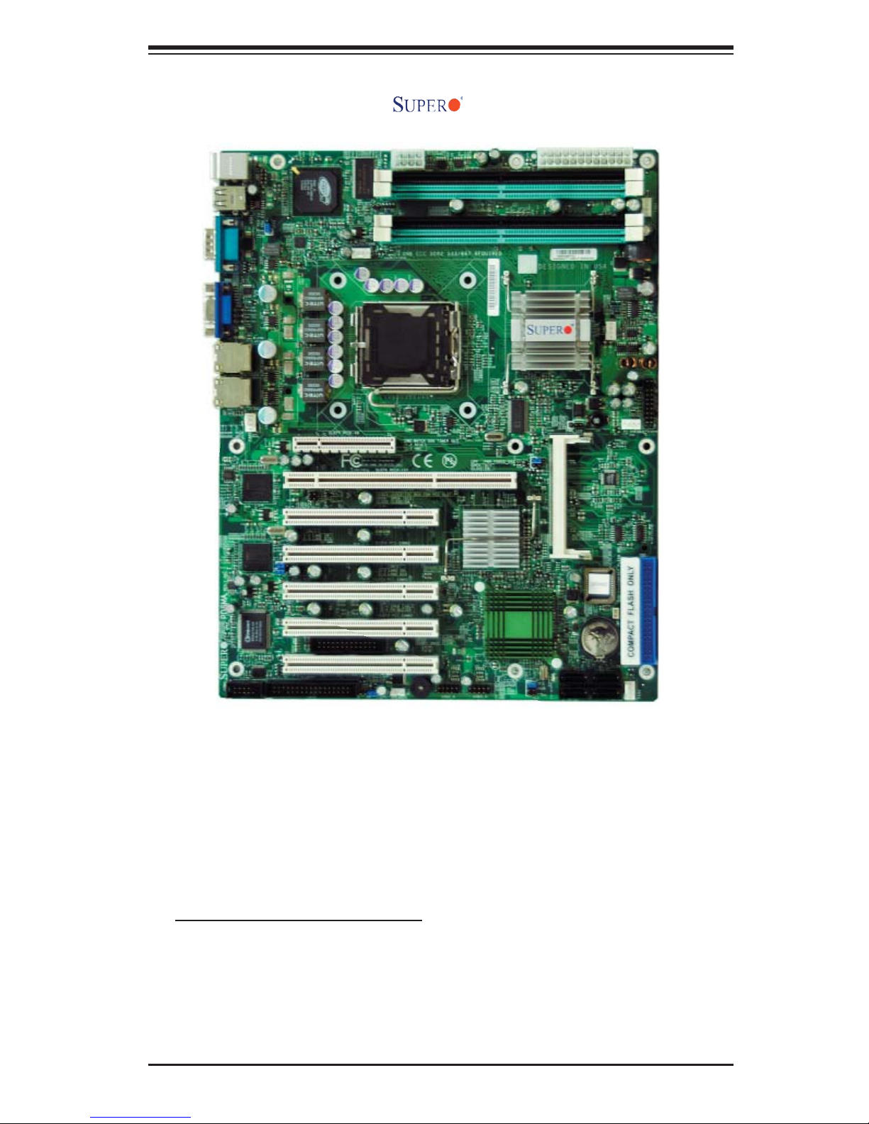
Figure 1-1. PDSMA Image
Chapter 1: Introduction
An Important Note to the User
• All images and layouts shown in this manual were based upon the latest PCB
Revision available at the time of publishing of this manual. The motherboard
you've received may or may not look exactly the same as the graphics shown
in this manual.
1-3
PDSMA User’s Manual
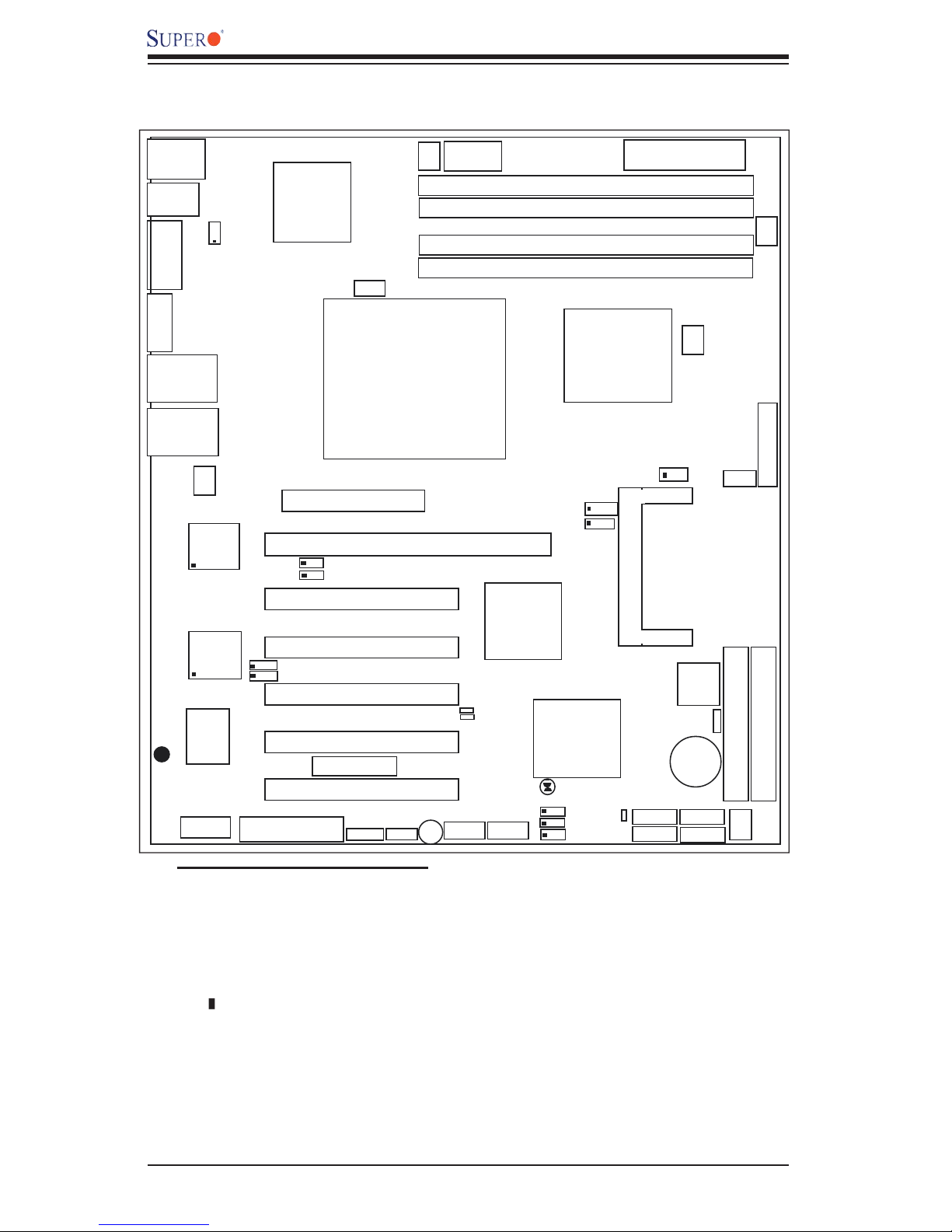
Figure 1-3. Motherboard Layout
(not drawn to scale)
KB/MS
J28
VGA
USB 1/2
J15
COM1
JPG1
CTRL
J31
VGA
JG1
JLAN1
JLAN2
Fan5
LAN1
CTRL
LAN2
CTRL
S I/O
®
Slot6
Slot5
Slot4
JPL1
JPL2
Slot3
Slot2
Slot7
PCI-Exp. x8
PCI-X 133 MHz
JI2C1
JI2C2
PCI 32-bit 33 MHz
PCI 32-bit 33 MHz
PCI 32-bit 33 MHz
PCI 32-bit 33 MHz
Printer
UPER PDSMA
COM2
S
Slot1
J27
PCI 32-bit 33 MHz
Floppy
J9
Important Notes to the User
Fan6
CPU
LGA 775
SPKR
WOL
PW3
DIMM 4
DIMM 3
DIMM 2
DIMM 1
JPW2
LE3
LE4
USB5/6
8-pin PWR
PXH-V
USB3/4
J46J45
DIMM 2B
DIMM 1B
DIMM 2A
DIMM 1A
Mukilteo
E7230
North Bridge
JWD
JPF
ICH7R
South Bridge
JBT1
JP3
JWOR
JL1
24-Pin ATX PWR
JPW1
Fan2
JLED
IPMI 2.0
BIOS
JWF1
Battery
SATA0
LE1
SATA1
SATA2
SATA3
Fan1
FP CTRL
Fan3
JF1
Primary IDE
*Compact Flash only
J4
J3
Fan4
• All images and graphics shown in this manual were based upon the latest
PCB Revision available at the time of publishing of this manual. The motherboard you've received may or may not look exactly the same as the graphics
shown in this manual.
• See Chapter 2 for detailed information on jumpers, I/O ports and JF1 frontpanel connections.
• " " indicates the location of "Pin 1".
• When the LE1 LED is on, the 5V Standby PWR is on. Maker sure to turn off
the power before installing or removing components.
• J4 (the white slot) is reserved for Compact Flash Card only. Do not use it for
other devices. If J4 is populated with a Compact Flash Card, J3 (the blue
slot) will be available for one device only; if not, J3 can be used for multiple
devices.
1-4

Chapter 1: Introduction
PDSMA Quick Reference (See Chapter 2 for details.)
Jumpers Description Default Setting
JBT1 CMOS Clear See Section 2-7
JP3 Compact Flash Master/Slave Closed (Master) (*Note 2)
JI2C1/JI2C2 SMbus to PCI Slot Open/Open (Disabled)
JPF Power Force-On Open (Disabled)
JPG1 VGA Enable Pins 1-2 (Enabled)
JPL1/JPL2 Giga-bit LAN 1/LAN 2 Enable Pins 1-2 (Enabled)
JWD Watch Dog Enable Pins 1-2 (Reset)
Connectors Description
24-PIn ATX (JPW1) ATX 24-Pin Power Connector
8-Pin PWR (JPW2) 12V 8-pin Power Connector (Required)
COM1(J31), COM2 COM Port 1 & COM 2 Header
DIMM#1A,#2A,#1B,#2B Memory (DIMM) Slots (1 through 4)
Fans 1-6 System Fan Headers (Fans 1-5), Fan6: CPU Fan
FP Control (JF1) Front Panel Control Header
Floppy Connector (J27) Floppy Disk Connector
GLAN1/2 (JLAN1/2) Ethernet RJ45 (Gigabit LAN) Port1/Port2 Connectors
IDE(J3)/Compact Flash (J4) J3: IDE Master/J4: Compact Flash Card*
IPMI IPMI 2.0 Socket
J9 Speaker Connector (Pins 3-4: Internal Buzzer, Pins 1-4:
External Speaker Cable)
JL1 Chassis Intrusion Header
JLED Power LED
JWF1 Compact Flash Card PWR Connector (*Note 2)
KB/MS (J28) PS/2 Keyboard/Mouse Connector
Printer (J30) Parallel Port (Printer) Header
Power Fault (PW3) Power Fault Header (*See Chapter 2)
SATA 0-3 (I-SATA 0-3) Intel SATA Headers: ISATA0-ISATA3
SPKR Internal Buzzer
Slot 1-Slot 5 PCI 32-bit 33MHz slots
Slot 6/Slot 7 PCI-X 64-bit 133MHz (Slot 6)/PCI-Exp x8 (Slot 7)
USB1/2 (J15) Back Panel Universal Serial Bus Ports 1,2
USB3/4 (J46),USB5/6 (J45) Front Panel Accessible USB headers 3,4,5,6
VGA (JG1) VGA Connector
WOL (WOL) Wake On LAN header
WOR (JWOR) Wake On Ring header
LED Indicator Description (*(Refer to Addendum A)
LE 1 Onboard Standby PWR warning LED Indicator
LE3/LE4 BIOS POST Code Indicators
*Notes: 1. J4 (the white slot) is reserved for Compact Flash Card only. Do not use it
for other devices. If J4 is populated with a Compact Flash Card, J3 (the blue slot) will
be available for one device only; if not, J3 can be used for multiple devices. 2. For
JP3 to work properly, you need to connect the CF card PWR cable to JWF1 fi rst.
1-5

PDSMA User’s Manual
Motherboard Features
CPU Latest CPU technology!
• Single Intel Pentium 4/Pentium D (Dual Core) LGA (Land Grid Array) 775
Processors at system bus speeds of 1066 MHz/800 MHz/533 MHz.
• Hyper-Threading (HT), EM64T, Enhanced Intel SpeedStep (EIST) supported
Using the EM64T Feature
• Use a CPU that supports the EM64T Technology
• Install a 64-bit OS (Windows XP Professional x64 Ed, Server 2003x64 Ed.)
• Install the 64-bit drivers for all MB components, devices and add-on cards
Using the Hyper-Threading (HT) Technology
• Use a CPU that supports Hyper-Threading Technology
• Install an OS that supports HT, including Windows XP/2003 Server and Linux
2.4x. (Under Linux, use the HT compiler to compile the code. For other oper-
ating systems, be sure to disable the HT feature in the BIOS.)
• Enable the HT feature in the BIOS (under "Advanced" Setting) before install-
ing a supported OS. (*Note: visit www.Intel.com for CPU support and driver
updates.)
• OS Licensing Support
• Intel Dual-Core CPU supports: Windows 2000 Professional, Windows
Advanced Server, Windows XP Home, Windows XP Professional, Windows
Server 2003 (Standard, Enterprise)
• Intel Dual-Core CPU and Hyper-Threading Technology supports: Windows
2000 Advanced Server, Windows XP Home, Windows XP Professional,
Windows Server 2003 (Standard, Enterprise)
Memory Latest memory technology! (*
• Four DIMM slots support Dual/Single Channel DDR2 667/533/400 MHz up to
8 GB of Unbuffered ECC/Non ECC two-way interleaved SDRAM.
Chipset Latest Intel chipset technology!
• Intel E7230 (Mukilteo)
• Intel ICH7R
• Intel PXH-V
Expansion Slots
• Five (5) PCI 32-Bit/33 MHz (Slot 1- Slot 5)
• One (1) PCI-X 64-Bit 133 MHz (Slot 6)
• One (1) PCI-Exp x8 (Slot 7)
BIOS
• 8Mb Firmware Hub Phoenix BIOS
• APM 1.2, DMI 2.3, PCI 2.2, PCI-X 1.0,ACPI 1.0, Plug and Play (PnP), SM-
BIOS 2.3, Hardware BIOS Virus Protection
Note: See Section 2-4 for details.)
1-6

Chapter 1: Introduction
PC Health Monitoring
• Onboard voltage monitors for CPU cores, Chipset Voltage, Memory
Voltage,+3.3V, +3.3V Standby,+5V, +5V Standby, +12V, −12V and VBAT
• CPU 4-phase-switching voltage regulator
• Status monitor for fan speed & System OH/Fan Fail LED
• Pulse Width Modulation Fan Control & Low noise fan speed control
• Environmental temperature monitoring via BIOS, PWR-Up from AC PWR loss
• SuperDoctor III, NMI
• System Resource alert via SuperDoctor III
ACPI Features
• Slow blinking LED for suspend state indicator
• BIOS support for USB keyboard
• Main switch override mechanism
• Internal/external modem ring-on
Onboard I/O
• 1 ATA/100 EIDE Channel
• Intel ICH7R SATA Controller, 4 connectors for 4 devices with support of RAID
functions 0, 1, 5 and 10
• 1 fl oppy port interface (up to 2.88 MB)
• 1 Fast UART 16550 compatible serial port and 1 header
• Two Intel single-port Gigabit Ethernet Controllers: 82573E(AMT)/82573L
• PS/2 mouse and PS/2 keyboard ports
• Up to 6 USB (Universal Serial Bus) 2.0 ports
• VGA Connector
• IPMI 2.0 Socket
• Super I/O (Winbond W83627 HF) with hardware monitoring (W83792D)
• ATI Rage XL 8 MB
Temperature
• Monitoring CPU, chassis environment
• CPU Thermal Trip support
• Thermal Monitor 2 (TM2) (available if supported by the CPU)
Other
• Wake-on-LAN (WOL)
• Wake-on-Ring (WOR)
• Onboard Standby PWR warning LED Indicator ("LE 1")
CD Utilities
• Drivers and software for Intel E7230 chipset utilities
Dimensions
• 9.6" (W) x 12" (L) (243.84 mmx 304.8 mm)
1-7
PDSMA User’s Manual
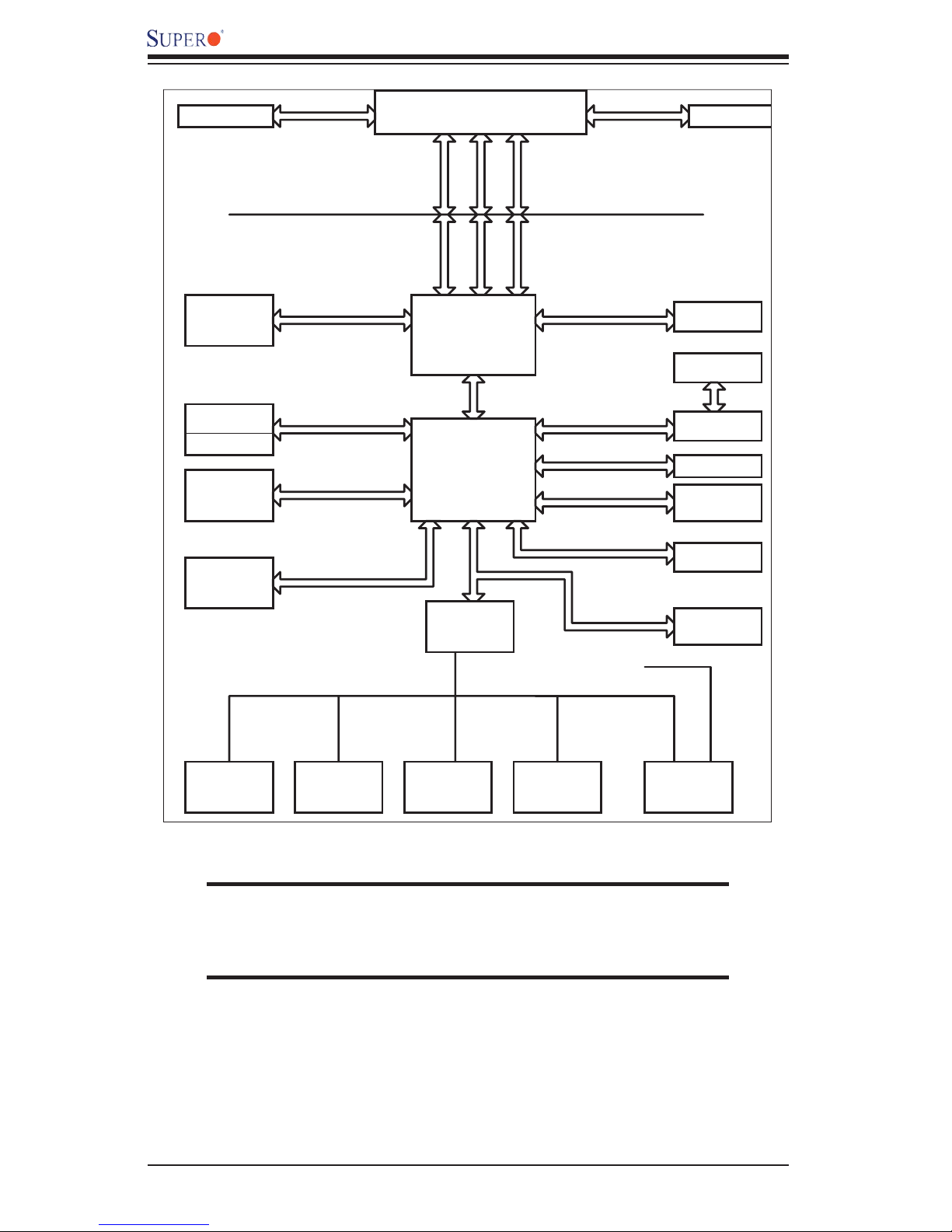
VRM 10.1
FSB: 1066/800/533MHz
DDR2
CH_A1-2
CH_B1-2
PRI_IDE
CF_HEADER
4 x SATA
PORTS
USB
PORT_0~7
VRM V10.1
DDR2_667/533/400
UDMA/100
S-ATA/3Gb
USB 2.0/1.1
LGA775_PROCESSOR
ADDR
CTRL CTRL
ADDR
MUKILTEO(E7230)
MCH
DMI
ICH-7R
LPC
W83627HF
LPC I/O
DATADATA
PCI-X BUS
PCIE_x4
PCIE_x1
PCI_32_BUS
PCI_32_BUS
CK410 CLK
1x PCIE_x8PCIE_x8
SLOT
1x PCIX_64
SLOT
PXH_V
2XGb_LAN
ATI
RAGE XL
5x PCI_32
SLOT
FWH
SMBUS I/F
KB. FDD. SER.1
MS.
Note: This is a general block diagram and may not exactly represent
the features on your motherboard. See the following pages for the
actual specifi cations of the motherboard.
SER.2
PRN.
Figure 1-3. E7230 Mukilteo Chipset:
System Block Diagram
1-8
H/W
MONITOR

Chapter 1: Introduction
1-2 Chipset Overview
Intel’s Mukilteo (E7230) chipset, designed for use with the Pentium 4/Pendium D
Processor in the LGA 775 Land Grid Array Package, is comprised of two primary
components: the Memory Controller Hub (MCH) and the I/O Controller Hub (ICH7R).
The PDSMA provides the performance and feature-set required for the high-end
server and the UP workstation market.
Memory Controller Hub (MCH)
The function of the MCH is to manage the data fl ow between four interfaces: the
CPU interface, the DDR2 System Memory Interface, the PCI Express Interface, and
the Direct Media Interface (DMI). The MCH is optimized for the Pentium 4/Pentium
D processor in the 90nm process in the LGA775 Land Grid Array Package. It sup-
ports one or two channels of DDR2 SDRAM.
The I/O Controller (ICH7R) provides the data buffering and interface arbitration re-
quired for the system to operate effi ciently. It also provides the bandwidth needed
for the system to maintain its peak performance. The Direct Media Interface (DMI)
provides the connection between the MCH and the ICH7R. The ICH7R supports
multiple PCI-Express slots, four Serial ATA ports, six USB 2.0 ports and two IDE
devices. In addition, the ICH7R offers the Intel Matrix Storage Technology which
provides various RAID options for data protection and rapid data access. It also
supports the next generation of client management in conjunction with the next
generation Gigabit Ethernet controller.
Intel ICH7R System Features
The I/O Controller Hub provides the I/O subsystem with access to the rest of the
system. Functions and capabilities include:
*Advanced Confi guration and Power Interface, Version 2.0 (ACPI)
*Intel IIO External Design Specifi cation (EDS)
*Mukilteo Memory Controller Hub (MCH) External Design Specifi cation (EDS)
*Intel I/O Controller Hub 7 (ICH7R) Thermal Design Guideline
*Low Pin Count (LPC) Interface
1-9

PDSMA User’s Manual
1-3 PC Health Monitoring
This section describes the PC health monitoring features of the PDSMA. The
motherboard has an onboard System Hardware Monitor chip that supports PC
health monitoring.
Onboard Voltage Monitors for the CPU Cores, Chipset Voltage,
Memory Voltage , +3.3V, +3.3V Standby, +5V, +5V Standby, +12V,
and −12V (via SuperO Doctor III)
The onboard voltage monitor will scan these voltages continuously. Once a voltage
becomes unstable, it will give a warning or send an error message to the screen.
The user can adjust the voltage thresholds to defi ne the sensitivity of the voltage
monitor.
Fan Status Monitor with Firmware Speed Control
The PC health monitor can check the RPM status of the cooling fans. The onboard
fans are controlled by Thermal Management via BIOS.
CPU Overheat/Fan Fail LED and Control
This feature is available when the user enables the CPU overheat warning option
in the BIOS. This allows the user to defi ne an overheat temperature. When this
temperature reaches the threshold, the CPU thermal trip feature will be activated,
and it will send a signal to the Speaker LED and, at the same time, the CPU speed
will decrease. It will also activate the alarm if a fan failure occurs.
1-4 Power Confi guration Settings
This section describes the features of Power Confi guration and Power Management
of your motherboard.
Slow Blinking LED for Suspend-State Indicator
When the CPU goes into a suspend state, the chassis power LED will start blinking
to indicate that the CPU is in the suspend mode. When the user presses any key, the
CPU will "wake-up" and the LED will automatically stop blinking and is turned on.
BIOS Support for USB Keyboard
If the USB keyboard is the only keyboard in the system, it will function like a normal
keyboard during system boot-up.
Main Switch Override Mechanism
When an ATX power supply is used, the power button can function as a system
suspend button. When the user presses the power button, the system will enter
a SoftOff state. The monitor will be suspended and the hard drive will spin down.
1-10

Chapter 1: Introduction
Press the power button again to "wake-up" the whole system. During the SoftOff
state, the ATX power supply provides power to the required circuitry and keep the
system "alive." In case the system malfunctions and you want to turn off the power,
just press and hold the power button for 4 seconds. The power will turn off and no
power will be provided to the motherboard.
Wake Ring-On (WOR)
Wake-up events can be triggered by a device such as the external modem ringing
when the system is in the SoftOff state. Note that external modem ring-on can only
be used with an ATX 2.01 (or above) compliant power supply.
Wake-On-LAN (WOL)
Wake-On-LAN is defi ned as the ability of a management application to remotely
power up a computer that is powered off. Remote PC setup, up-dates and asset
tracking can occur after hours and on weekends so that daily LAN traffi c is kept to
a minimum and users are not interrupted. The motherboard has a 3-pin header
(WOL) to connect to the 3-pin header on a Network Interface Card (NIC) that has
WOL capability. Note that Wake-On-LAN can only be used with an ATX 2.01 (or
above) compliant power supply.
1-5 ACPI Features
ACPI stands for Advanced Confi guration and Power Interface. The ACPI specifi ca-
tion defi nes a fl exible and abstract hardware interface that integrates power man-
agement features with other components of a PC system, including its hardware,
operating system and application software. This enables the system to automati-
cally turn on and off peripherals such as CD-ROMs, network cards, hard disk drives
and printers. This also includes other devices connected to the PC such as VCRs,
TVs, telephones and stereos.
In addition to enabling operating system-directed power management, ACPI
provides a generic system event mechanism for Plug and Play and an operating
system-independent interface for confi guration control. ACPI leverages the Plug
and Play BIOS data structures while providing a processor architecture-independent
implementation that is compatible with both Windows and Linux Operating Systems.
1-6 Power Supply
As with all computer products, a stable power source is necessary for proper and
reliable operation. It is even more important for processors that have high CPU
clock rates of 1 GHz and faster.
1-11

PDSMA User’s Manual
The
PDSMA accommodates 12V ATX power supplies. Although most
power supplies generally meet the specifi cations required by the CPU, some are
inadequate. A 2 amps of current supply on a 5V Standby rail is strongly recom-
mended. It is strongly recommended that you use a high quality power supply that
meets ATX power supply Specifi cation 2.02 or above. Also your power supply must
supply 1.5A for the Ethernet ports. It must also be SSI compliant (info at http://www.
ssiforum.org/). Additionally, in areas where noisy power transmission is present,
you may choose to install a line fi lter to shield the computer from noise. It is recom-
mended that you also install a power surge protector to help avoid problems caused
by power surges. To provide adequate power supply to the system, the additional
8-pin 12V (JPW2) power is also required.
1-12

Chapter 2: Installation
Chapter 2
Installation
2-1 Static-Sensitive Devices
Electric-Static-Discharge (ESD) can damage electronic com ponents. To prevent
damage to your system board, it is important to handle it very carefully. The following
measures are generally suffi cient to protect your equipment from ESD.
Precautions
• Use a grounded wrist strap designed to prevent static discharge.
• Touch a grounded metal object before removing the board from the antistatic
bag.
• Handle the board by its edges only; do not touch its components, peripheral
chips, memory modules or gold contacts.
• When handling chips or modules, avoid touching their pins.
• Put the motherboard and peripherals back into their antistatic bags when not in
use.
• For grounding purposes, make sure your computer chassis provides excellent
conductivity between the power supply, the case, the mounting fasteners and
the motherboard.
Unpacking
The motherboard is shipped in antistatic packaging to avoid static damage. When
unpacking the board, make sure the person handling it is static protected.
2-1
PDSMA User's Manual
2-2 Processor and Heatsink Installation
When handling the processor package, avoid placing
direct pressure on the label area of the fan.
(*Notes: 1. Always connect the power cord last and always remove it before adding,
removing or changing any hardware components. Make sure that you install the
processor into the CPU socket before you install the CPU heatsink.
2. Intel's boxed Pentium 4 CPU package contains the CPU fan and heatsink as-
sembly. If you buy a CPU separately, make sure that you use only Intel-certifi ed
multi-directional heat sinks and fans.
3. The Intel Pentium 4/Pentium D LGA 775 heatsink and fan comes with a push-pin
design and no tool is needed for installation.
4. Make sure to install the motherboard into the chassis before you install the CPU
heatsink and fan.)
5. When purchasing an LGA 775 CPU or when receiving a motherboard with an LGA
775 CPU pre-installed, make sure that the CPU plastic cap is in place and none of
the CPU pins are bent; otherwise, contact the retailer immediately.
!
6. Refer to the MB Features Section for more details on CPU support.
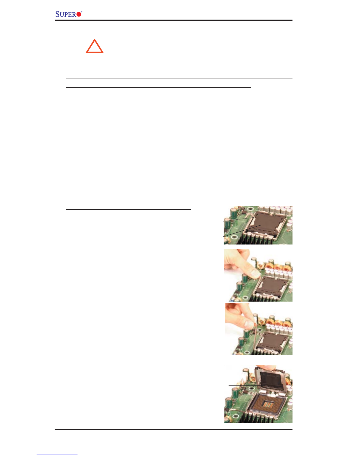
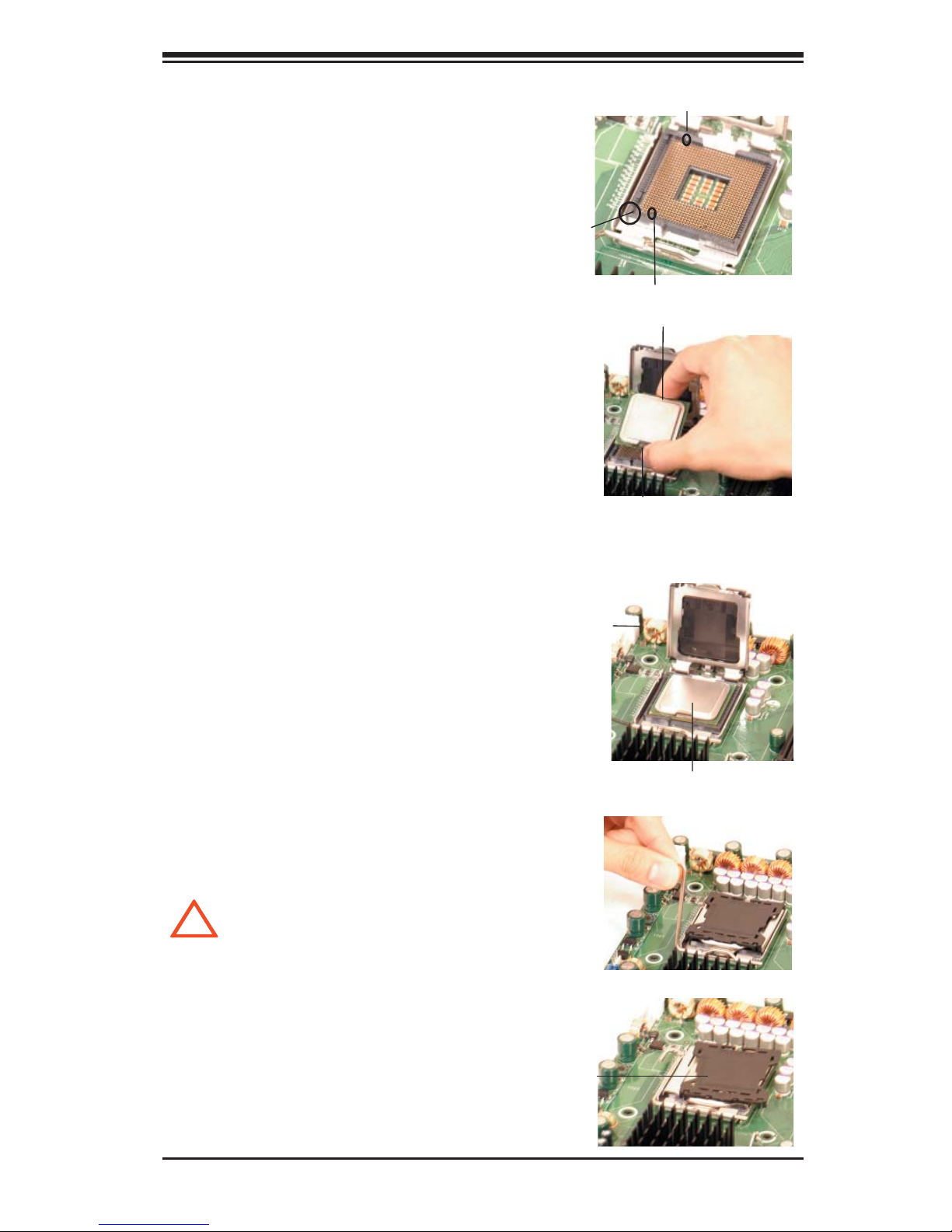
Installation of the LGA775 Processor
Socket Lever
Load Plate
1. Press the socket lever to release the
load plate that covers the CPU socket
from its locking position.
2. Gently lift the socket lever to open
the load plate.
Load Plate
2-2
Chapter 2: Installation
3. Locate Pin 1 on the CPU socket. (*Note:
Pin 1 is the corner marked with a triangle).
Please note that the North Key and the
South Key are located vertically in the
CPU housing.
4. Position the motherboard in such a way
that Pin 1 of the CPU socket is located at
the left bottom of the CPU housing.
5. Use your thumb and your index fi nger to
hold the CPU at the North Center Edge and
the South Center Edge of the CPU.
6. Align Pin 1 of the CPU with Pin 1 of the
socket. Once aligned, carefully lower the
CPU straight down to the socket. (**Do not
drop the CPU on the socket. Do not move
the CPU horizontally or vertically. Do not
rub the CPU against the surface or against
any pins of the socket to avoid damage to
the CPU or the socket.)
North Key
Pin 1
South Key
North Center Edge
South Center Edge
7. With the CPU inside the socket, inspect
the four corners of the CPU to make sure
that the CPU is properly installed.
8. Use your thumb to gently push the lever
down and lock it in the hook.
9. If the CPU is properly installed in the
socket, the plastic cap will be automatically
released from the load plate when the lever
is pushed into the hook. Remove the plastic
cap from the motherboard.
(*Warning: Please keep the plastic
!
cap. The motherboard and the CPU
must be shipped with the plastic cap prop-
erly installed to protect the CPU pins. Ship-
ment without the CPU plastic cap properly
installed will void the warranty.)
Plastic cap is released from
the load plate if the CPU is
properly installed.
Socket Lever
CPU in the CPU socket
2-3
PDSMA User's Manual
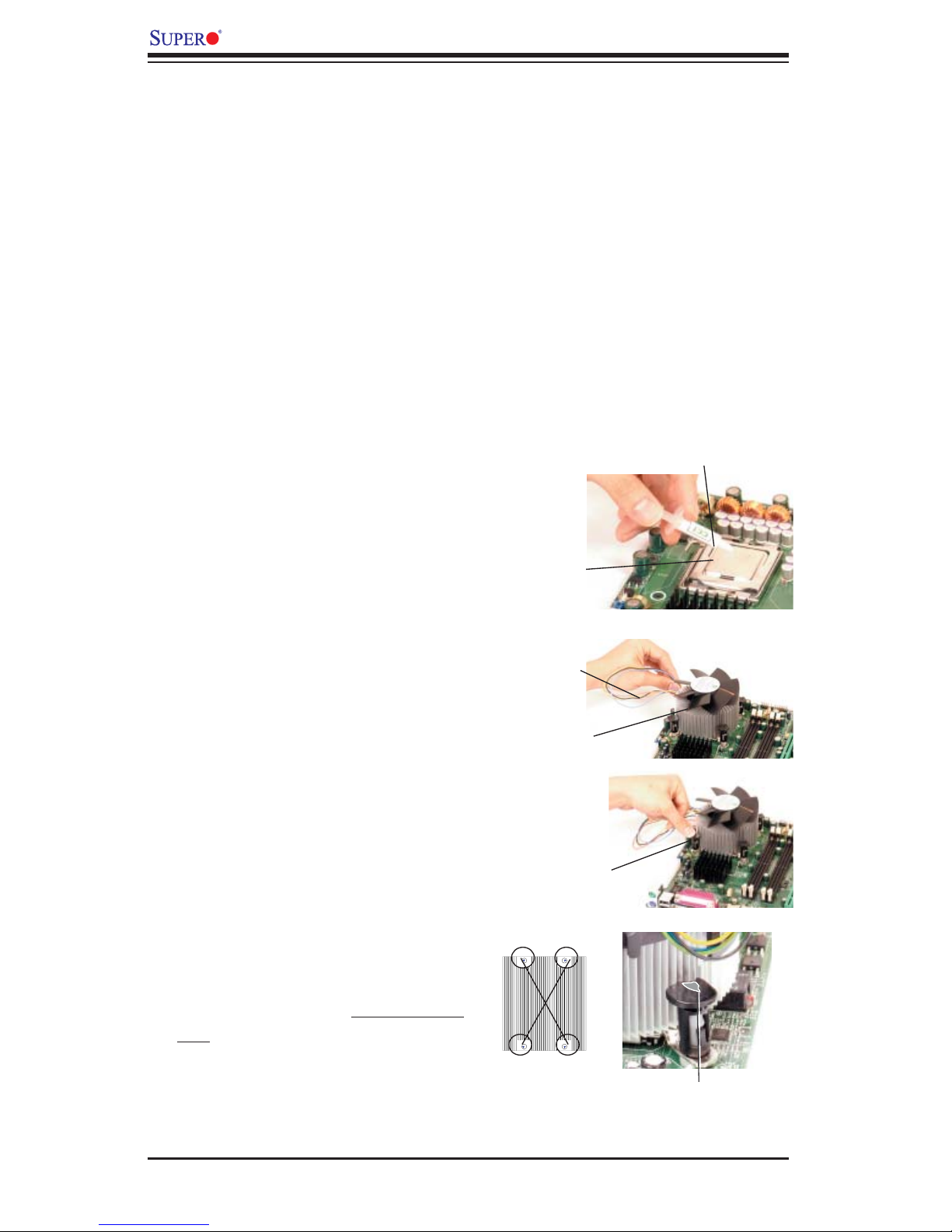
Installation of the Heatsink
1. Locate the CPU Fan on the moth-
erboard. (Refer to the layout on Page
1-4 for the CPU Fan location.)
2. Position the heatsink in such a way
that the heatsink fan wires are closest
to the CPU fan and are not interfered
with other components.
3. Inspect the CPU Fan wires to make
sure that the wires are routed through
the bottom of the heatsink.
4. Remove the thin layer of the protec-
tive fi lm from the copper core of the
heatsink.
Thermal Grease
(*Warning: CPU overheat may occur if
the protective fi lm is not removed from
the heatsink.)
5. Apply the proper amount of thermal
grease on the CPU. (*Note: if your
heatsink came with a thermal pad,
please skip this step.)
6. If necessary, rearrange the wires
to make sure that the wires are not
pinched between the heatsink and the
CPU. Also make sure to keep clear-
ance between the fan wires and the
fi ns of the heatsink.
7. Align the four heatsink fasteners
with the mounting holes on the mother-
board. Gently push the pairs of diago-
nal fasteners (#1 & #2, and #3 & #4)
into the mounting holes until you hear a
click. (*Note: Make sure to orient each
fastener in a way that the narrow end of
the groove is pointing outward.)
CPU
Fan Wires
Heatsink Fins
Heatsink
Fastener
#1
#4
#3
#2
Narrow end of the groove
points outward
2-4
8. Repeat Step 6 to insert all four heatsink
fasteners into the mounting holes.
9. Once all four fasteners are securely
inserted into the mounting holes and the
heatsink is properly installed on the moth-
erboard, connect the heatsink fan wires to
the CPU Fan connector.
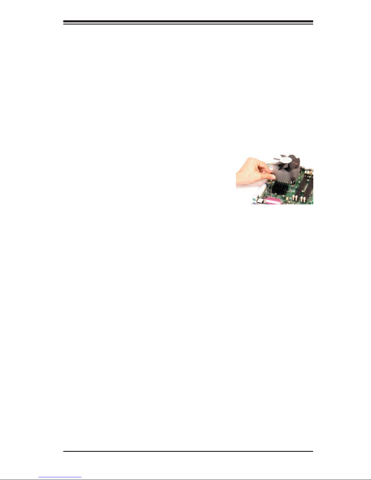
Heatsink Removal
1. Unplug the power cord from the power
supply.
2. Disconnect the heatsink fan wires from
the CPU fan header.
3. Use your fi nger tips to gently press on
the fastener cap and turn it counterclock-
wise to make a 1/4 (90
the fastener upward to loosen it.
0
) turn, and then pull
Chapter 2: Installation
4. Repeat Step 3 to loosen all fasteners
from the mounting holes.
5. With all fasteners loosened, remove the
heatsink from the CPU.
2-3 Mounting the Motherboard in the Chassis
All motherboards have standard mounting holes to fi t different types of chassis.
Make sure that the locations of all the mounting holes for both the motherboard and
the chassis match. Although a chassis may have both plastic and metal mounting
fasteners, metal ones are highly recommended because they ground the mother-
board to the chassis. Make sure that the metal standoffs click in or are screwed in
tightly. Then use a screwdriver to secure the motherboard onto the motherboard
tray. (*Note: some components are close to the mounting holes. Please take all
necessary precautionary measures to prevent damage done to these components
when installing the motherboard into the chassis.)
2-5
PDSMA User's Manual
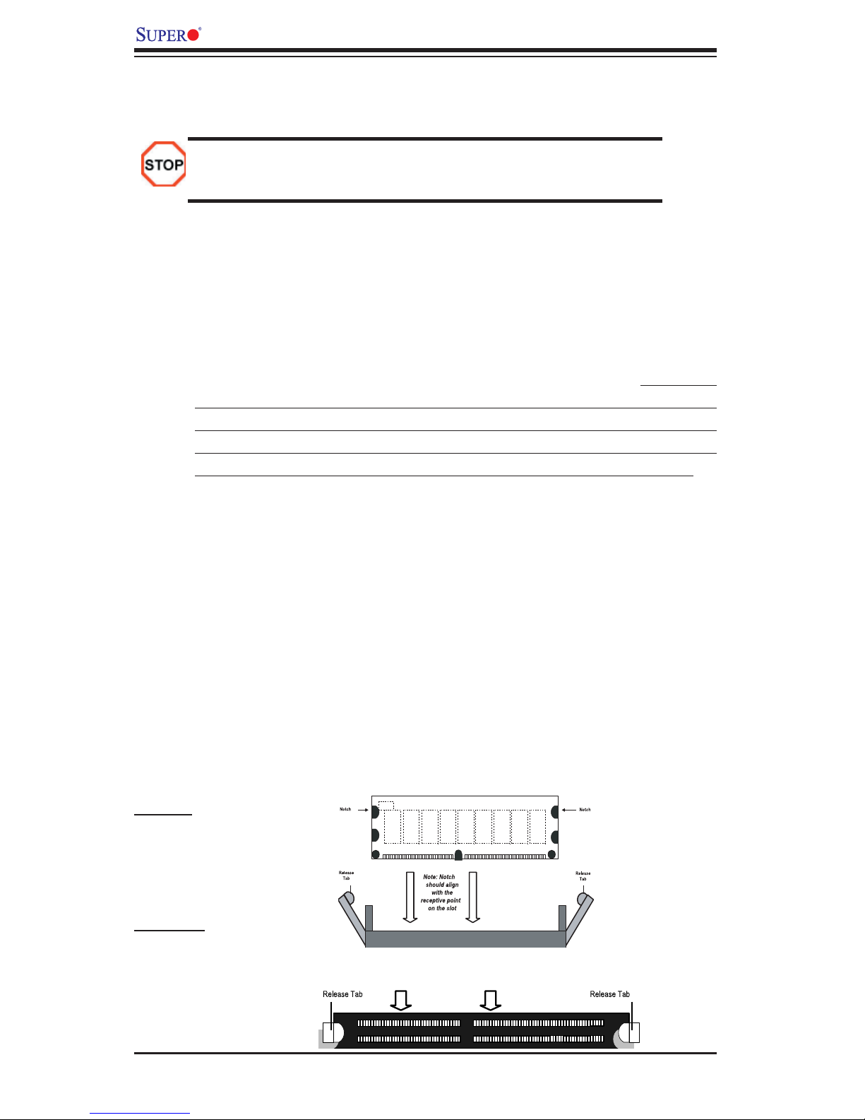
2-4 Installing DDR II Memory
Memory Module Installation (See Figure 2-2)
Exercise extreme care when installing or removing memory modules
to prevent any possible damage.
1. Insert each DDR II memory module vertically into its slot. Pay attention to the
notch along the bottom of the module to prevent inserting the module incor-
rectly. (See support information below.)
2. Gently press down on the memory module until it snaps into place.
Support
The PDSMA supports up to 8 GB of Dual channel, ECC/Non-ECC unbuffered
DDRII 667/533/400 SDRAM. Both interleaved and non-interleaved memory
are supported, so you may populate any number of DIMM slots. (Populating
DIMM#1A,DIMM#1B, and/or DIMM#2A, DIMM#2B with modules of the same
size and of the same type will result in dual channel, two-way interleaved
memory which is faster than the single-channel non-interleaved memory. When
ECC memory is used, it may take 25-40 seconds for the VGA to display.)
*Notes:
1. Due to chipset limitation, 8GB Memory can only be supported by the following
operating systems: 32-Bit: Windows 2000 Advanced Server/ 2003 Enterprise
Edition; 64-Bit: Windows Server 2003 Standard/XP Professional x64 Edition/
Server 2003 Enterprise (x64 Edition.)
2. You may install a maximum of 2GB DIMMs on each slot; however, only DDRII
533 MHz 2GB density modules are available for this confi guration.
3. Some old-version of DDR II-667 may not match Intel's On-Die-Temperature
requirement and will automatically be down-graded to run @ 533 MHz, If this
occurs, contact your memory vendor to check the ODT value.
4. Due to OS limitations, some operating systems may not show more than 4 GB
of memory. (See the Memory Availability on Page 2-7.)
Figure 2-2. Installing DIMM into Slot
To Install:
Insert module vertically and press down
until it snaps into
place. Pay attention
to the notch.
DDR2
To Remove:
Use your thumbs to
gently push each
release tab outward
to release the DIMM
from the slot.
Top View Of DDRII Slot
2-6
n
Possible System Memory Allocation & Availability
Chapter 2: Installation
System Device Size Physical Memory Remaining (-Available)
Firmware Hub fl ash memory (System BIOS) 1 MB 3.99GB
Local APIC 4 KB 3.99GB
Area Reserved for the chipset 2 MB 3.99GB
I/O APIC (4 Kbytes) 4 KB 3.99GB
PCI Enumeration Area 1 256 MB 3.76GB
PCI Express (256 MB) 256 MB 3.51GB
PCI Enumeration Area 2 (if needed) -Aligned on
256 MB boundary-
VGA Memory 16 MB 2.85GB
TSEG 1 MB 2.84GB
Memory available for the OS & other applications 2.84GB
512 MB 3.01GB
(4 GB Total System Memory)
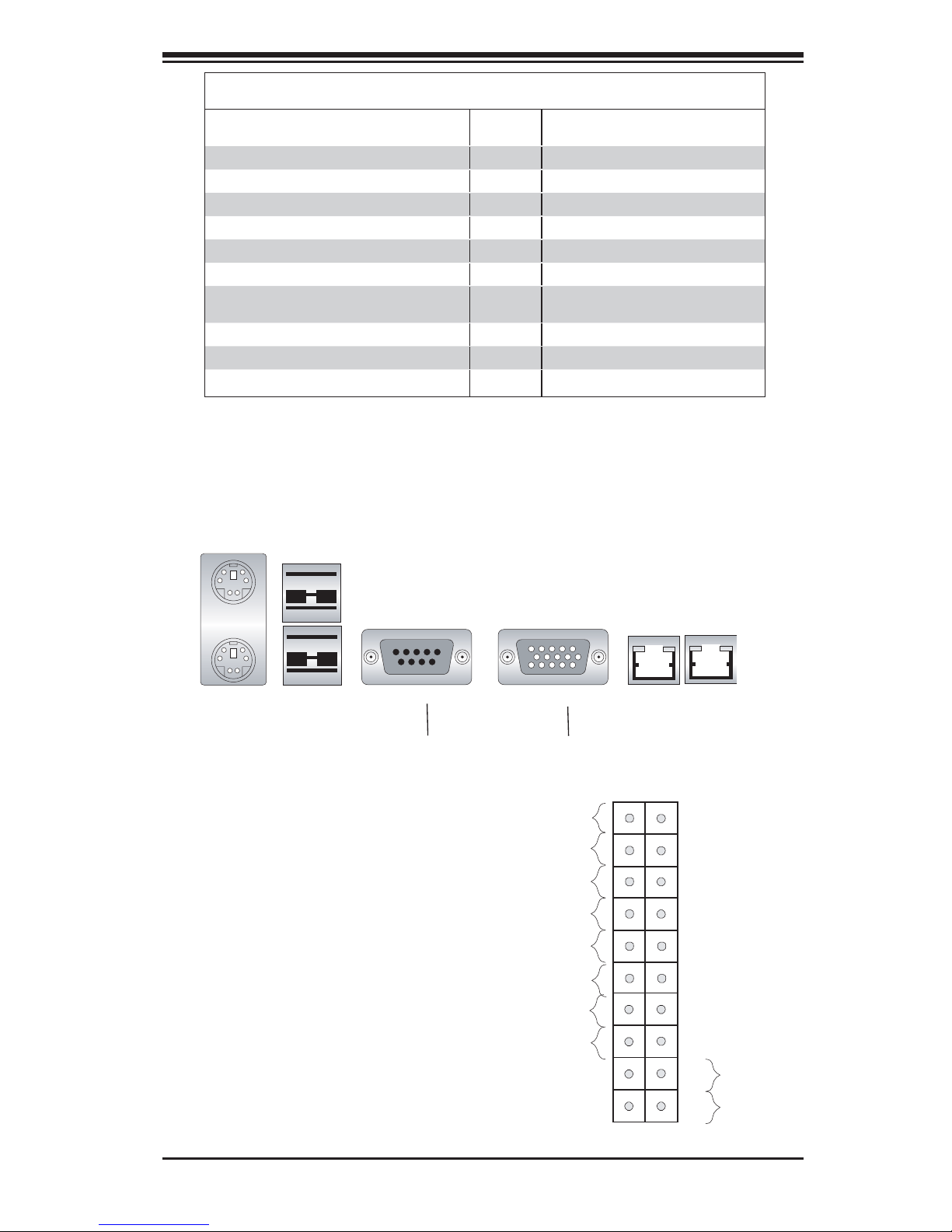
2-5 I/O Port/Control Panel Connector Locations
The I/O ports are color coded in conformance with the PC99 specifi cation to make
setting up your system easier. See Figure 2-3 below for the colors and locations
of the various IO ports.
Figure 2-3. I/O Port Locations and Defi nitions
Mouse (Green)
KB (Purple)
USB 0/1
COM1
(Green)
Front Control Panel
JF1 contains header pins for various
buttons and indicators that are nor-
mally located on a control panel at
the front of the chassis. These con-
nectors are designed specifi cally for
use with Supermicro server chassis.
See Figure 2-4 for the descriptions of
the various control panel buttons and
LED indicators. Refer to the follow-
ing section for descriptions and pin
defi nitions.
VGA
(Blue)
Ground
X
Power LED
HDD LED
NIC1 LED
NIC2 LED
OH/Fan Fail LED
X
Ground
Ground
LAN 1/LAN2
1920
2
1
Figure 2-4. JF1 Header Pins
NMI
X
Vcc
Vcc
Vcc
Vcc
Vcc
Vcc
Reset
PWR
Reset Button
Power Butto
2-7
PDSMA User's Manual
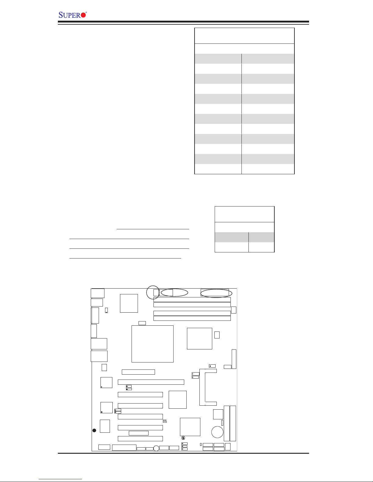
2-6 Connecting Cables
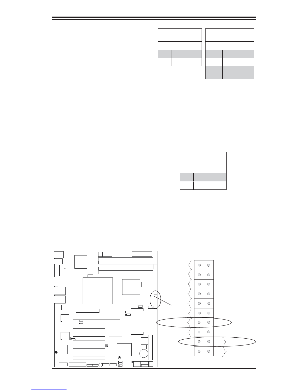
ATX Power Connector
The main power supply connector
(JPW1) on the PDSMA meets the SSI
(Superset ATX) specifi cation. You can
only use a 24-pin power supply cable on
the motherboard. Make sure that the ori-
entation of the connector is correct. You
must also use the 8-pin (JPW2) proces-
sor power connector to provide adequate
power supply to the system. See the
table on the right for pin defi nitions.
ATX Power 24-pin Connector
Pin Defi nitions
Pin# Defi nition Pin # Defi nition
13 +3.3V 1 +3.3V
14 -12V 2 +3.3V
15 COM 3 COM
16 PS_ON 4 +5V
17 COM 5 COM
18 COM 6 +5V
19 COM 7 COM
20 Res (NC) 8 PWR_OK
21 +5V 9 5VSB
22 +5V 10 +12V
23 +5V 11 +12V
24 COM 12 +3.3V
Processor Power Connector
In addition to the Primary ATX power con-
nector (above), the 12V 8-pin Processor
connector at JPW2 must also be con-
nected to your power supply to provide
adequate power supply to the system.
KB/MS
J28
USB 1/2
J15
JPG1
COM1
J31
VGA
JG1
JLAN1
JLAN2
Fan5
LAN1
CTRL
LAN2
CTRL
S I/O
®
UPER PDSMA
J27
COM2
S
4-Pin 12V PWR
VGA
CTRL
Fan6
Slot7
PCI-Exp. x8
Slot6
PCI-X 133 MHz
JI2C1
JI2C2
Slot5
PCI 32-bit 33 MHz
Slot4
PCI 32-bit 33 MHz
JPL1
JPL2
Slot3
PCI 32-bit 33 MHz
Slot2
PCI 32-bit 33 MHz
Printer
Slot1
PCI 32-bit 33 MHz
Floppy
J9
CPU
LGA 775
SPKR
WOL
PW3
DIMM 4
DIMM 3
DIMM 2
DIMM 1
JPW2
USB5/6
LE3
LE4
USB3/4
J46J45
8-pin PWR
DIMM 2B
DIMM 1B
DIMM 2A
DIMM 1A
PXH-V
ICH7R
South Bridge
JBT1
JP3
Mukilteo
E7230
North Bridge
JWD
JPF
JWOR
JL1
CPU Power Connector
Pin Defi nitions
Pins Defi nition
1 through 4 Ground
5 through 8 +12V
24-Pin ATX PWR8-Pin 12V PWR
JLED
IPMI 2.0
SATA0
SATA1
BIOS
Battery
SATA2
SATA3
Fan2
JPW1
Fan3
JWF1
*Compact Flash only
J4
Fan4
24-Pin ATX PWR
LE1
Fan1
FP CTRL
JF1
Primary IDE
J3
2-8
Chapter 2: Installation
n
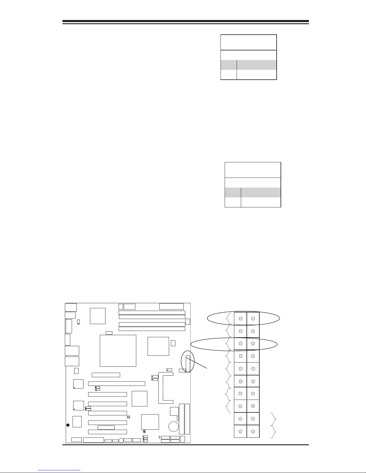
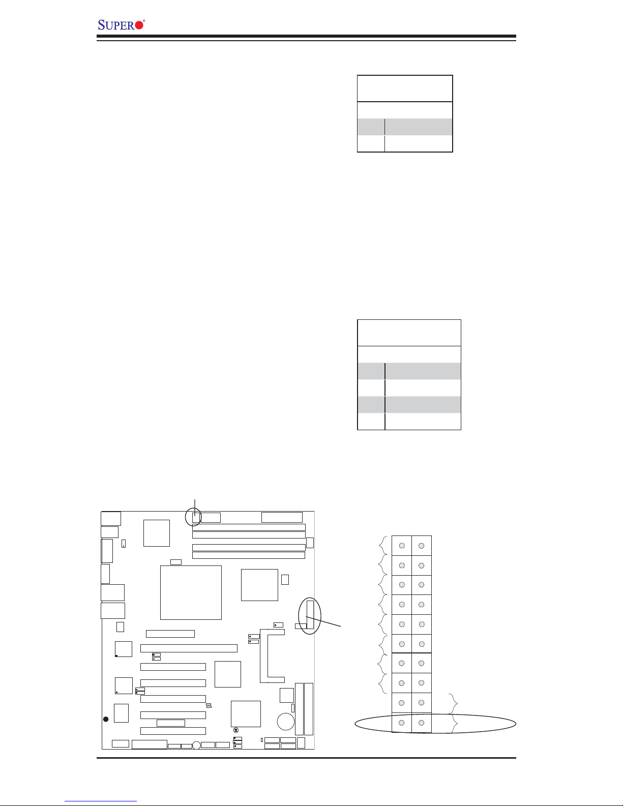
NMI Button
The non-maskable interrupt button
header is located on pins 19 and 20
of JF1. Refer to the table on the right
for pin defi nitions.
Power LED
The Power LED connection is located
on pins 15 and 16 of JF1. Refer to the
table on the right for pin defi nitions.
NMI Button
Pin Defi nitions (JF1)
Pin# Defi nition
19 Control
20 Ground
Power LED
Pin Defi nitions (JF1)
Pin# Defi nition
15 +5V
16 Ground
KB/MS
J28
USB 1/2
J15
JPG1
COM1
J31
VGA
JG1
JLAN1
JLAN2
Fan5
LAN1
CTRL
LAN2
CTRL
S I/O
®
J27
COM2
SUPER PDSMA
VGA
CTRL
Slot7
Slot6
PCI-X 133 MHz
Slot5
PCI 32-bit 33 MHz
Slot4
PCI 32-bit 33 MHz
JPL1
JPL2
Slot3
PCI 32-bit 33 MHz
Slot2
PCI 32-bit 33 MHz
Slot1
PCI 32-bit 33 MHz
Floppy
PCI-Exp. x8
JI2C1
JI2C2
Printer
Fan6
J9
CPU
LGA 775
SPKR
WOL
PW3
DIMM 4
DIMM 3
DIMM 2
DIMM 1
JPW2
USB5/6
LE3
LE4
8-pin PWR
PXH-V
USB3/4
J46J45
DIMM 2B
DIMM 1B
DIMM 2A
DIMM 1A
Mukilteo
North Bridge
JWD
JPF
ICH7R
South Bridge
JBT1
JP3
JWOR
JL1
24-Pin ATX PWR
E7230
JLED
IPMI 2.0
SATA0
LE1
SATA1
JPW1
Fan2
Fan3
OH/Fan Fail LED
BIOS
JWF1
Battery
*Compact Flash only
J4
J3
SATA2
SATA3
Fan4
2-9
PWR LED
Fan1
Power LED
HDD LED
FP CTRL
NIC1 LED
JF1
NIC2 LED
Primary IDE
Ground
X
X
Ground
Ground
NMI
1920
NMI
X
Vcc
Vcc
Vcc
Vcc
Vcc
Vcc
Reset
2
1
PWR
Reset Button
Power Butto
PDSMA User's Manual
n
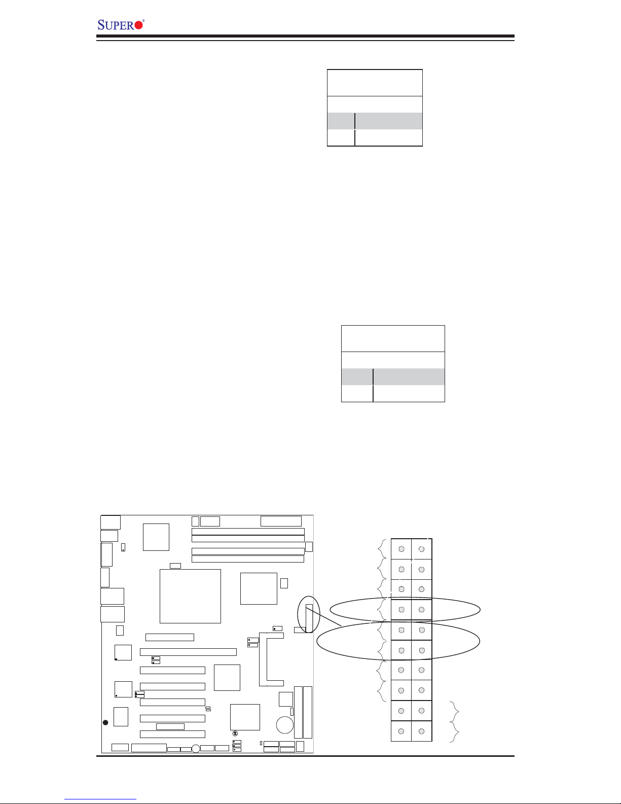
HDD LED
The HDD LED connection is located
on pins 13 and 14 of JF1. Attach the
hard drive LED cable here to display
disk activities (including Serial ATA
and IDE drive activities). See the
table on the right for pin defi nitions.
NIC1/NIC2 LED Indicators
HDD LED
Pin Defi nitions (JF1)
Pin# Defi nition
13 +5V
14 HD Active
The NIC (Network Interface Control-
ler) LED connections for the GLAN
port1 is located on pins 11 and 12 of
JF1, and for the GLAN port2 is located
on pins 9 and 10 of JF1. Attach the
NIC LED cables to display network
activity. Refer to the table on the right
for pin defi nitions.
WOL
SPKR
PW3
DIMM 4
DIMM 3
DIMM 2
DIMM 1
JPW2
USB5/6
LE3
LE4
J46J45
8-pin PWR
PXH-V
USB3/4
DIMM 2B
DIMM 1B
DIMM 2A
DIMM 1A
Mukilteo
North Bridge
JWD
JPF
ICH7R
South Bridge
JBT1
JP3
JWOR
JL1
24-Pin ATX PWR
E7230
LE1
KB/MS
J28
USB 1/2
J15
JPG1
COM1
J31
VGA
JG1
JLAN1
JLAN2
Fan5
LAN1
CTRL
LAN2
CTRL
S I/O
®
J27
COM2
SUPER PDSMA
VGA
CTRL
Slot7
Slot6
PCI-X 133 MHz
Slot5
Slot4
PCI 32-bit 33 MHz
JPL1
JPL2
Slot3
PCI 32-bit 33 MHz
Slot2
PCI 32-bit 33 MHz
Slot1
PCI 32-bit 33 MHz
Floppy
Fan6
CPU
LGA 775
PCI-Exp. x8
JI2C1
JI2C2
PCI 32-bit 33 MHz
Printer
J9
JLED
IPMI 2.0
SATA0
SATA1
BIOS
Battery
SATA2
SATA3
Fan2
JPW1
Fan1
FP CTRL
Fan3
JF1
OH/Fan Fail LED
JWF1
Primary IDE
*Compact Flash only
J4
J3
Fan4
GLAN1/2 LED
Pin Defi nitions (JF1)
Pin# Defi nition
9/11 Vcc
10/12 Ground
HDD LED
NIC1/NIC2 LED
Ground
X
Power LED
HDD LED
NIC1 LED
NIC2 LED
X
Ground
Ground
1920
NMI
X
Vcc
Vcc
Vcc
Vcc
Vcc
Vcc
Reset
Reset Button
Power Butto
PWR
2
1
2-10
Chapter 2: Installation
n
Overheat/FanFail LED
Connect an LED cable to the OH/Fan
Fail connection on pins 7 and 8 of
JF1 to provide advanced warnings
of chassis overheating or system fan
failure. Refer to the table on the right
for pin defi nitions.
Reset Button
The Reset Button connection is lo-
cated on pins 3 and 4 of JF1. Attach
it to the hardware reset switch on the
computer case. Refer to the table on
the right for pin defi nitions.
OH/Fan Fail LED
Pin Defi nitions (JF1)
Pin# Defi nition
7 Vcc
8 Ground
Reset Button
Pin Defi nitions (JF1)
Pin# Defi nition
3 Reset
4 Ground
OH/Fan Fail Indicator
Status
State Defi nition
Off Normal
On Overheat
Flash-
Fan Fail
ing
KB/MS
J28
USB 1/2
J15
JPG1
COM1
J31
VGA
JG1
JLAN1
JLAN2
Fan5
LAN1
CTRL
LAN2
CTRL
S I/O
®
J27
COM2
SUPER PDSMA
VGA
CTRL
Slot7
Slot6
Slot5
Slot4
JPL1
JPL2
Slot3
Slot2
Slot1
PCI 32-bit 33 MHz
Floppy
PCI-Exp. x8
PCI-X 133 MHz
JI2C1
JI2C2
PCI 32-bit 33 MHz
PCI 32-bit 33 MHz
PCI 32-bit 33 MHz
PCI 32-bit 33 MHz
Printer
Fan6
J9
CPU
LGA 775
SPKR
WOL
PW3
DIMM 4
DIMM 3
DIMM 2
DIMM 1
JPW2
USB5/6
LE3
LE4
8-pin PWR
PXH-V
USB3/4
J46J45
DIMM 2B
DIMM 1B
DIMM 2A
DIMM 1A
Mukilteo
North Bridge
JWD
JPF
ICH7R
South Bridge
JBT1
JP3
JWOR
JL1
24-Pin ATX PWR
E7230
JLED
IPMI 2.0
SATA0
LE1
SATA1
BIOS
Battery
SATA2
SATA3
Fan2
JPW1
Fan1
FP CTRL
Fan3
JF1
OH/Fan Fail LED
JWF1
Primary IDE
*Compact Flash only
J4
J3
Fan4
2-11
OH/Fan Fail LED
Ground
X
Power LED
HDD LED
NIC1 LED
NIC2 LED
X
Ground
Ground
1920
Reset
NMI
X
Vcc
Vcc
Vcc
Vcc
Vcc
Vcc
Reset
Reset Button
Power Butto
PWR
2
1
PDSMA User's Manual
n
Power Button
The Power Button connection is
located on pins 1 and 2 of JF1. Mo-
mentarily contacting both pins will
power on/off the system. This button
can also be confi gured to function as
a suspend button (with a setting in
BIOS - see Chapter 4). To turn off the
power when set to suspend mode,
press the button for at least 4 sec-
onds. Refer to the table on the right
for pin defi nitions.
Power Fault
Connect a cable from your power
supply to the Power Fault header
(PW3) to provide warnings of power
supply failure. This warning signal is
passed through the PWR_LED pin
to indicate of a power failure on the
chassis. See the table on the right for
pin defi nitions.
Power Button
Pin Defi nitions (JF1)
Pin# Defi nition
1 Signal
2 +3V Standby
PWR Fault
Pin Defi nitions
Pin# Defi nition
1 Pin 1 Fail Signal
2 Pin 2 Fail Signal
3 Pin 3 Fail Signal
4 Pin 4 Fail Signal
Note: This feature is only available when using
redundant Supermicro power supplies.
PWR Fault
WOL
SPKR
PW3
DIMM 4
DIMM 3
DIMM 2
DIMM 1
JPW2
USB5/6
KB/MS
J28
USB 1/2
J15
JPG1
COM1
J31
VGA
JG1
JLAN1
JLAN2
Fan5
LAN1
CTRL
LAN2
CTRL
S I/O
®
J27
COM2
SUPER PDSMA
VGA
CTRL
Slot7
Slot6
PCI-X 133 MHz
Slot5
Slot4
PCI 32-bit 33 MHz
JPL1
JPL2
Slot3
PCI 32-bit 33 MHz
Slot2
PCI 32-bit 33 MHz
Slot1
PCI 32-bit 33 MHz
Floppy
Fan6
CPU
LGA 775
PCI-Exp. x8
JI2C1
JI2C2
PCI 32-bit 33 MHz
Printer
J9
LE3
LE4
J46J45
8-pin PWR
PXH-V
USB3/4
DIMM 2B
DIMM 1B
DIMM 2A
DIMM 1A
Mukilteo
North Bridge
JWD
JPF
ICH7R
South Bridge
JBT1
JP3
JWOR
JL1
24-Pin ATX PWR
E7230
JLED
IPMI 2.0
SATA0
LE1
SATA1
BIOS
Battery
SATA2
SATA3
Fan2
JPW1
Fan1
FP CTRL
Fan3
JF1
OH/Fan Fail LED
JWF1
Primary IDE
*Compact Flash only
J4
J3
Fan4
2-12
Ground
Power LED
HDD LED
NIC1 LED
NIC2 LED
Ground
X
X
Ground
PWR Button
1920
NMI
X
Vcc
Vcc
Vcc
Vcc
Vcc
Vcc
Reset
Reset Button
Power Butto
PWR
2
1
 Loading...