

Supermicro PDSLA, PDSLE User Manual

PDSLA
PDSLE
USER’S MANUAL
Revision 1.1c

The information in this User’s Manual has been carefully reviewed and is believed to be accurate.
The vendor assumes no responsibility for any inaccuracies that may be contained in this document,
makes no commitment to update or to keep current the information in this manual, or to notify any
person or organization of the updates. Please Note: For the most up-to-date version of this
manual, please see our web site at www.supermicro.com.
Super Micro Computer, Inc. ("Supermicro") reserves the right to make changes to the product
described in this manual at any time and without notice. This product, including software, if any,
and documentation may not, in whole or in part, be copied, photocopied, reproduced, translated or
reduced to any medium or machine without prior written consent.
IN NO EVENT WILL SUPER MICRO COMPUTER, INC. BE LIABLE FOR DIRECT, INDIRECT,
SPECIAL, INCIDENTAL, SPECULATIVE OR CONSEQUENTIAL DAMAGES ARISING FROM THE
USE OR INABILITY TO USE THIS PRODUCT OR DOCUMENTATION, EVEN IF ADVISED OF
THE POSSIBILITY OF SUCH DAMAGES. IN PARTICULAR, SUPER MICRO COMPUTER, INC.
SHALL NOT HAVE LIABILITY FOR ANY HARDWARE, SOFTWARE, OR DATA STORED OR USED
WITH THE PRODUCT, INCLUDING THE COSTS OF REPAIRING, REPLACING, INTEGRATING,
INSTALLING OR RECOVERING SUCH HARDWARE, SOFTWARE, OR DATA.
Any disputes arising between manufacturer and customer shall be governed by the laws of Santa
Clara County in the State of California, USA. The State of California, County of Santa Clara shall
be the exclusive venue for the resolution of any such disputes. Super Micro's total liability for all
claims will not exceed the price paid for the hardware product.
FCC Statement: This equipment has been tested and found to comply with the limits for a Class B
digital device pursuant to Part 15 of the FCC Rules. These limits are designed to provide reasonable
protection against harmful interference in a residential installation. This equipment generates,
uses, and can radiate radio frequency energy and, if not installed and used in accordance with the
manufacturer’s instruction manual, may cause interference with radio communications. However,
there is no guarantee that interference will not occur in a particular installation. If this equipment
does cause harmful interference to radio or television reception, which can be determined by turning
the equipment off and on, you are encouraged to try to correct the interference by one or more of
the following measures:
*Reorient or relocate the receiving antenna.
*Increase the separation between the equipment and the receiver.
*Connect the equipment into an outlet on a circuit different from that to which the receiver is
connected.
*Consult the dealer or an experienced radio/television technician for help.
California Best Management Practices Regulations for Perchlorate Materials: This Perchlorate
warning applies only to products containing CR (Manganese Dioxide) Lithium coin cells. “Perchlorate
Material-special handling may apply. See www.dtsc.ca.gov/hazardouswaste/perchlorate”.
WARNING: Handling of lead solder materials used in this
product may expose you to lead, a chemical known to
the State of California to cause birth defects and other
reproductive harm.
Manual Revision 1.1c
Release Date: July 18, 2008
Unless you request and receive written permission from Super Micro Computer, Inc., you may not
copy any part of this document.
Information in this document is subject to change without notice. Other products and companies
referred to herein are trademarks or registered trademarks of their respective companies or mark
holders.
Copyright © 2008 by Super Micro Computer, Inc.
All rights reserved.
Printed in the United States of America

Preface
Preface
About This Manual
This manual is written for system integrators, PC technicians and
knowledgeable PC users. It provides information for the installation and use of
the
Intel Pentium® D/Pentium® 4/Celeron Processor in the 775-Land Grid Array Pack-
age at a system bus speed of 1066/800/533 MHz. The Intel Pentium® D/Pentium®
4/Celeron Processor in the 775-Land Grid Array Package is housed in a Flip-Chip
Land Grid Array (FC-LGA4) package that interfaces with the motherboard via an
LGA775 socket. The package consists of a processor core mounted on a substrate
land-carrier. An integrated heat spreader (IHS) is attached to the package substrate
and core and serves as the contacting surface for processor component thermal
solutions, such as a heatsink. Please refer to the motherboard specifi cations pages
on our web site (http://www.supermicro.com/Products) for updates on supported
processors. This product is intended to be professionally installed.
PDSLA/PDSLE motherboard. The PDSLA/PDSLE supports a single
Manual Organization
Chapter 1 includes a checklist of what should be included in your mainboard box,
describes the features, specifi cations and performance of the PDSLA/PDSLE main-
board and provides detailed information about the chipset.
Chapter 2 begins with instructions on handling static-sensitive devices. Read
this chapter when installing the processor, memory modules and mounting the
mainboard in the chassis. Also refer to this chapter for other hardware and software
installation.
If you encounter any problems, see Chapter 3, which describes troubleshooting
procedures for video connection, memory modules and CMOS setup. For quick
reference, a general FAQ (Frequently Asked Questions) section is provided. Instruc-
tions are also included for contacting technical support. In addition, you can visit our
web site at www.supermicro.com/techsupport.htm for more detailed information.
Chapter 4 provides detailed information on running the CMOS Setup utility.
Appendix A provides BIOS Error Beep Codes.
Appendix B lists BIOS POST Codes.
iii
PDSLA/PDSLE User’s Manual
Table of Contents
Preface
About This Manual ...................................................................................................... iii
Manual Organization ................................................................................................... iii
Chapter 1: Introduction
1-1 Overview ......................................................................................................... 1-1
Checklist ..................................................................................................... 1-1
Contacting Supermicro ............................................................................... 1-2
PDSLA/PDSLE Image ............................................................... 1-3
PDSLA/PDSLE Layout ............................................................... 1-4
PDSLA/PDSLE Quick Reference ................................................ 1-5
Intel 945G/P Chipset: System Block Diagram ........................................... 1-6
Motherboard Features .............................................................................. 1-7
1-2 Chipset Overview ........................................................................................... 1-9
1-3 PC Health Monitoring ................................................................................... 1-10
1-4 Power Confi guration Settings ....................................................................... 1-11
1-5 Power Supply ............................................................................................... 1-12
1-6 Super I/O ........................................................................................................ 1-13
Chapter 2: Installation
2-1 Static-Sensitive Devices ................................................................................. 2-1
2-2 Processor and Heatsink Installation ............................................................... 2-2
2-3 Mounting the Motherboard in the Chassis ..................................................... 2-5
2-4 Installing DDR 2 Memory ............................................................................... 2-6
2-5 I/O Port/Front Control Panel Connector Locations ........................................ 2-7
2-6 Connecting Cables ......................................................................................... 2-8
Power Supply Connectors ...................................................................... 2-8
Power On Connector ................................................................................ 2-9
Reset Connector ...................................................................................... 2-9
Overheat/Fan Fail LED ......................................................................... 2-10
NIC1 LED Connector .............................................................................. 2-10
HDD LED ................................................................................................. 2-11
Power_LED Connector ............................................................................ 2-11
Serial Ports ............................................................................................. 2-12
CD Header/Aux Audio Header ............................................................... 2-12
iv

Table of Contents
Front Panel Audio ..................................................................................... 2-13
Ethernet Port ............................................................................................ 2-13
Fan Headers ............................................................................................. 2-14
Chassis Intrusion ...................................................................................... 2-14
ATX PS/2 Keyboard/Mouse Ports ......................................................... 2-15
Universal Serial Bus (USB) ..................................................................... 2-15
Wake-On-Ring .......................................................................................... 2-16
Wake-On-LAN .......................................................................................... 2-16
VGA Connector ........................................................................................ 2-17
AC'97 Output ............................................................................................ 2-17
2-7 Jumper Settings ............................................................................................ 2-18
Explanation of Jumpers ......................................................................... 2-18
CMOS Clear ........................................................................................... 2-18
USB Wake-Up .......................................................................................... 2-19
Watch Dog Enable/Disable ...................................................................... 2-20
Gigabit LAN Enable .................................................................................. 2-20
SMBus to PCI/PCI-Express Slots ............................................................ 2-21
Speaker Connector .................................................................................. 2-21
CPU Front Side Bus Speed ..................................................................... 2-22
2-8 Onboard LED Indicators ................................................................................ 2-23
GLAN LEDs .............................................................................................. 2-23
Power LED ................................................................................................ 2-23
2-9 Parallel Port, Floppy/Hard Drive and Audio Connections ............................ 2-24
Parallel Port Connector ........................................................................... 2-24
Floppy Connector ................................................................................... 2-25
IDE Connector .......................................................................................... 2-25
2-10 Installing the Operating System and Software Programs ............................. 2-26
Chapter 3: Troubleshooting
3-1 Troubleshooting Procedures ........................................................................... 3-1
Before Power On ....................................................................................... 3-1
No Power ................................................................................................... 3-1
No Video .................................................................................................. 3-1
Memory Errors ........................................................................................... 3-2
Losing the System’s Setup Confi guration ................................................ 3-2
3-2 Technical Support Procedures ....................................................................... 3-2
3-3 Frequently Asked Questions .......................................................................... 3-3
3-4 Returning Merchandise for Service ................................................................. 3-5
v

PDSLA/PDSLE User’s Manual
Chapter 4: BIOS
4-1 Introduction ....................................................................................................... 4-1
4-2 Running Setup ................................................................................................. 4-2
4-3 Main BIOS Setup ............................................................................................. 4-2
Main BIOS Setup Menu ........................................................................... 4-3
4-4 Advanced BIOS Setup ...................................................................................... 4-5
4-4.1 Advanced BIOS Features ................................................................ 4-5
4-4.2 Advanced Chipset Control ............................................................... 4-6
4-4.3 I/O Device Confi guration .................................................................. 4-8
4-4.4 PnP Confi guration .......................................................................... 4-10
4-4.5 Hardware Monitors ......................................................................... 4-11
4-4.6 Processor & Clock Options ............................................................ 4-11
4-5 Security ........................................................................................................... 4-12
4-6 Boot ............................................................................................................... 4-13
4-7 Exit ................................................................................................................. 4-15
Appendices:
Appendix A: BIOS Error Beep Codes .......................................................................A-1
Appendix B: BIOS POST Codes ................................................................................B-1
vi

Chapter 1: Introduction
Chapter 1
Introduction
1-1 Overview
Checklist
Congratulations on purchasing your computer motherboard from an acknowledged
leader in the industry. Supermicro boards are designed with the utmost attention to
detail to provide you with the highest standards in quality and performance.
Please check that the following items have all been included with your motherboard.
If anything listed here is damaged or missing, contact your retailer.
All items are included in the retail box.
One (1) Supermicro Mainboard
Two (2) SATA cables
One (1) IDE cable
One (1) fl oppy drive ribbon cable
One (1) I/O shield
One (1) Supermicro CD containing drivers and utilities
One (1) User's/BIOS Manual
1-1

PDSLA/PDSLE User’s Manual
Contacting Supermicro
Headquarters
Address: Super Micro Computer, Inc.
980 Rock Ave.
San Jose, CA 95131 U.S.A.
Tel: +1 (408) 503-8000
Fax: +1 (408) 503-8008
Email: marketing@supermicro.com (General Information)
support@supermicro.com (Technical Support)
Web Site: www.supermicro.com
Europe
Address: Super Micro Computer B.V.
Het Sterrenbeeld 28, 5215 ML
's-Hertogenbosch, The Netherlands
Tel: +31 (0) 73-6400390
Fax: +31 (0) 73-6416525
Email: sales@supermicro.nl (General Information)
support@supermicro.nl (Technical Support)
rma@supermicro.nl (Customer Support)
Asia-Pacifi c
Address: Super Micro Computer, Inc.
4F, No. 232-1 Liancheng Road
Chung-Ho 235, Taipei Hsien, Taiwan, R.O.C.
Tel: +886-(2) 8226-3990
Fax: +886-(2) 8226-3991
Web Site: www.supermicro.com.tw
Technical Support:
Email: support@supermicro.com.tw
Tel: 886-2-8228-1366, ext.132 or 139
1-2
PDSLA/PDSLE Image
Chapter 1: Introduction
An Important Note to the User
• All images and layouts shown in this manual are based upon the latest PCB
Revision available at the time of publishing of this manual. The motherboard
you've received may or may not look exactly the same as the ones shown in
this manual.
1-3
KB/MS
J31
VGA
JG1
USB
3/4/5/6
RJ45
USB1/2
Audio
J28
J41
4-Pin ATX PWR
COM1
Parallel Port
J30
(*PDSLA )
J44
J11
J45
PDSLA/PDSLE User’s Manual
Motherboard Layout
(not drawn to scale)
LGA 775 Processor
JFUSB1
JPUSB1
Fan3
Clock
Slot#7
PCI-E x1
JFUSB2
J
7
945G/P
(Lakeport)
North Bridge
Fan1/CPU
DIMM#1A
DIMM#2A
DIMM#2B
DIMM#1B
O
I/
r
e
p
Su
J40
J2 7
24-Pin ATX PW R
Floppy
LAN
CTRL
AC97
®
CD inAux.In
GLAN Enable
UPER DSLA/PDSLE
FP Aud
S
J12
Slot#6
Slot#5
Slot#4
PCI#4
Slot#3
PCI#3 -33MHz
Slot#2
PCI#2-33MHz
JPL1
Slot#1
PCI#1-33MHz
PCI-E x16
PCI-E x1
-33MHz
J
8
JP
1
JP
2
PC
PC
PC
F/P USB Wa ke- up
J
PC
PU
J1
COM2
J13
J
WO
R
I4
I3
I2
2
SB
BIOS
I
1
ICH7
South Bridge
CL CMOS
JBT1
F/P USB7/8
J43
I-SATA0
I-SATA1
4
WOL
D2
I-SATA2
I-SATA3
Buzzer
Battery
JL1
JLED
J9
JWD
LE 1
Fan 2
J3
JF 1
DE
I
Important Notes to the User
• See Chapter 2 for detailed information on jumpers, I/O ports and JF1 front panel
connections.
• " " indicates the location of "Pin 1".
• The only difference between the PDSLA and PDSLE is that the PDSLA has an
internal VGA.
CTRL
FP
1-4

Chapter 1: Introduction
PDSLA/PDSLE Quick Reference
Jumpers Description Default Setting
J9 Buzzer/Speaker Enable
JBT1 CMOS Clear (*See Chapter 2)
JFSB1/JFSB2 CPU Frequency Pins 1-2/Pins 1-2 (Auto)
JP1/JP2 PCI/PCI-E SMB Open/Open (Disabled)
JPL1 Giga-bit LAN Enable Pins 1-2 (Enabled)
JPUSB1 B/P USB Wake Up Pins 2-3 (Disabled)
JPUSB2 F/P USB Wake Up Pins 2-3 (Disabled)
JWD Watch Dog Pins 1-2 (Reset)
Connectors Description
ATX PWR (J40) ATX 24-Pin Power Connector
4-Pin ATX PWR (J41) 12V 4-pin Power Connector (*required)
Audio (J45) Audio Port
AUX-In (AUX1) Auxiliary (Audio) Input Header
CD-In (CD1) Audio CD Input Header
Chassis Intrusion(JL1) Chassis Intrusion Header
COM1 (J31), COM2 (J13) COM Port/Serial Port 1 & Port 2 Connectors
DIMM#1A,#2A,#1B,#2B Memory (DIMM) Slots (1 through 4)
Fans 1-3 Fan1: CPU Fan, Fan2/3: Chassis Fan Headers
Floppy (J27) Floppy Disk Connector
FP Audio (J12) Front Panel Audio Connector (*See Chapter 2)
FP Control Panel (JF1) Front Control Panel Header
LAN Port (J11) Ethernet RJ45 (Gigabit LAN) Connector
IDE (J3) IDE Connector
I-SATA #0-3 (J2,J4,J5,J6) Intel SATA (#0-3) Headers
KB/Mouse (J28) PS/2 Keyboard/Mouse
LE1 Standby Warning LED Indicator
PWR LED (JLED) Power LED Indicator
Printer (J30) Parallel Printer Port
Slot 1-Slot 4 PCI 33 MHz (PCI #1-#4)
Slot 5 PCI-Express x1 (using x 8 slot)
Slot 6 PCI-Express x16
Slot 7 PCI-Express x1
Speaker (J9) Speaker Header
USB 1/2 (J11) (Back Panel) Universal Serial Ports 1-2
USB 3/4/5/6 (J44) (Back Panel) Universal Serial Ports 3-6
USB 7/8 (J43) (Front Panel) USB ports 7/8
VGA (JG1) Video/Graphic Connector (*For PDSLA only)
WOL (WOL) Wake-On-LAN Header
WOR(JWOR) Wake-On-Ring Header
Pins 3-4 (Enabled)
1-5
PDSLA/PDSLE User’s Manual
VRM 10.1
INTEGRATED
GRAPHIC
(945G only)
1 PCIE_x16
GRAPHIC
PRI_IDE
4 x SATA
PORTS
USB
PORT_0~7
LGA775_PROCESSOR
VRM V10.1
FSB: 1066/800/533MHz
PCIE_x16
UDMA/100
S-ATA/300
ADDR
CTRL
LAKEPORT
945G/P
ICH-7
LPC
DMI
DATA
DDR2_667/533/400
PCIE_x1
PCIE_x1
PCI_32_BUS
AC97
LPCUSB 2.0/1.1
CK410 CLK
DIMM_CHA
DIMM_CHB
82573 LAN
1_PCIE_x1
SLOTS
1_PCIE_x8
SLOTS
4_PCI_x32
SLOTS
FWH
W83627HG 5.1-CH
LPC I/O
KB. FDD. SER.1
MS.
SER.2
AUDIO
PRN.
945G/P Lakeport Chipset:
System Block Diagram
Note: This is a general block diagram and may not exactly represent
the features on your motherboard. See the following pages for the
actual specifi cations of each motherboard.
1-6

Chapter 1: Introduction
Motherboard Features
CPU
®
• Single Intel Pentium
Package at a system bus speed of 1066/800/533 MHz.
• Supports Intel Hyper-Threading Technology.
Memory
• Supports unbuffered, non-ECC single or dual channel DDR2 with the bandwidth
up to 5.3GB/s (DDR2 667) for single channel mode and 10.7 GB/s (DDR2 667) in
dual-channel Interleaved mode.
Chipset
• Intel Lakeport 945G/P chipset
Expansion Slots
• One (1) PCI-Express x16 (intended for graphics)
• One (1) PCI-Express x8 (PCI-Express x1 Signal)
• One (1) PCI-Express x1
• Four (4) 32-bit PCI 33MHz (5V)
D/Pentium® 4/Celeron Dual Core in a 775-Land Grid Array
Note: See Section 2-4 for details.
BIOS
• 4 Mb Firmware Hub AwardBIOS
®
Flash BIOS
• APM 1.2, DMI 2.3, PCI 2.2, ACPI 1.0, Plug and Play (PnP)
PC Health Monitoring
• Onboard voltage monitors for Chipset Core +1.5V, CPU core, +3.3V, +3.3V
standby, +5V, +5V Standby, Vbat (battery voltage) and ±12V
• Fan status monitor with fi rmware 4 pin fan speed control
• Fan Fail Alert LED and Beep
• SuperDoctor III, Watch Dog, NMI
• Environmental temperature monitoring via BIOS
• Power-up mode control for recovery from AC power loss
• System overheat LED and control
• System resource alert via Supero Doctor III
• Auto-switching voltage regulator for the CPU core
ACPI Features
• Slow blinking LED for suspend state indicator
• BIOS support for USB keyboard
• Main switch override mechanism
• External modem ring-on
1-7
PDSLA/PDSLE User’s Manual
Onboard I/O
• 1 ATA/100 EIDE Channels for a total of two IDE devices backward compatible
• Built in ICH7 SATA Controller, 4 connectors for 4 devices (300MB/S)
• 1 fl oppy port interface (up to 2.88 MB)
• 2 Fast UART 16550 compatible serial ports
• Intel 82573V Gigabit Ethernet Controller
• 1 EPP (Enhanced Parallel Port) and ECP (Extended Capabilities Port) sup-
ported parallel port
• PS/2 mouse and PS/2 keyboard ports
• Up to 8 USB (Universal Serial Bus) 2.0 ports for a speed of up to 480Mbps
Latest USB 2.0 technology!
• AC'97 audio high quality 6-channel sound
• Integrated gfx core graphics on board (*PDSLA Only)
Other
• Wake-on-LAN
• Wake-on-Ring (WOR)
• System Bus Clock Frequency Selection (Overclocking) Support (*Note)
• Suspend-to-RAM
• Onboard +5V Standby Power Warning LED ("LE1")
• Pb Free
CD Utilities
• BIOS fl ash upgrade utility
• Drivers and software for Intel 945G/P chipset utilities
Dimensions
• ATX form factor, 11.5" x 9.5" (292 x 242 mm)
Note: Please be aware of the following conditions when over-
clocking is used:
Setting a high CPU FSB speed (overclocking), using a DRAM
frequency, or selecting a high CPU V-Core voltage, memory voltage, chipset volt-
age, ICH chipset voltage, or an FSB termination voltage may cause the system
to become unstable. If this occurs, reset the setting to the default setting. In ad-
dition, extra fans may be needed for proper system cooling. The PDSLA/PDSLE
offers the option of overclocking; however, Supermicro is not responsible for any
damage caused by the use of overclocking.
1-8

Chapter 1: Introduction
1-2 Chipset Overview
Intel’s Lakeport (945G/P) chipset consists of two primary components: the Graphics
Memory Controller Hub (GMCH)/Memory Controller Hub (MCH) and the I/O Control-
ler Hub (ICH7). Optimized for the Celeron, Pentium 4, Pentium D processors in an
LGA775 Package, the Lakeport (945G/P) provides the performance and feature-set
required for high-end UP dual core processor desktop solutions.
Graphics Memory Controller Hub (GMCH)/Memory
Controller Hub (GMCH)
The GMCH/MCH supports high-performance integrated graphics and manages the
data fl ow of the following fi ve interfaces: the CPU interface, DDR2 interface, PCI
Express Graphic Interface, the DMI (Direct Media Interface) and integrated graphics
with display interfaces (GMCH only) .The GMCH/MCH supports a FSB frequency
of 533/800/1066 MHz when used with a scalable CPU. It supports up to two chan-
nels of non-ECC DDR2 400/533/667 SDRAM. The integrated graphics controller
provides 3D, 2D and display capabilities. The GMCH/MCH also supports advanced
desktop power management.
Intel ICH7 System Features
The ICH7 provides extensive I/O support to a high-end 945G/P system. Functions
and capabilities include:
•
PCI Express Base Specifi cation, Rev. 1.0a-compliant
•
PCI 2.3 with support for 33 MHz PCI operations
•
ACPI Power Management Logic Support
•
Integrated Serial ATA host controller with independent DMA operation on four
ports, (with support of SATA I and SATA II HDD)
•
Integrated IDE controller supports Ultra ATA 100/66/33
USB host interface with support for eight USB ports
•
Enhanced DMA Controller, interrupt controller, and timer functions
•
System Management Bus (SMBus) 2.0 with additional support for I
•
vices
•
Low Pin Count (LPC) Interface
•
Firmware Hub (FWH) Interface
•
Audio Codec '97 Rev. 2.3 which provides a link for Audio (up to 6 channels)
2
C de-
1-9

PDSLA/PDSLE User’s Manual
1-3 PC Health Monitoring
This section describes the PC health monitoring features of the PDSLA/PDSLE.
The motherboard has an onboard System Hardware Monitor chip that supports
PC health monitoring.
Recovery from AC Power Loss
BIOS provides a setting for you to determine how the system will respond when
AC power is lost and then restored to the system. You can choose for the system
to remain powered off (in which case you must hit the power switch to turn it back
on) or for it to automatically return to a power on state. See the Power Lost Control
setting in the BIOS chapter of this manual to change this setting. The default set-
ting is Last State.
Onboard Voltage Monitoring
The onboard voltage monitor will scan the following voltages continuously: CPU
Core, Chipset Core +1.5V, +3.3V, +3.3V standby, +5V, +5V Standby, Vbat and
±12V. Once a voltage becomes unstable, it will give a warning or send an error
message to the screen. Users can adjust the voltage thresholds to defi ne the sen-
sitivity of the voltage monitor by using SD III.
Fan Status Monitor with Software
The PC health monitor can check the RPM status of the cooling fans via Supero
Doctor III.
Fan Fail Alert
When a fan fails during the normal operation, the Fan Fail LED will start to blink
and the buzzer will be activated to indicate a fan failure.
CPU Overheat LED and Control
This feature is available when the user enables CPU overheat warning in the BIOS.
This allows the user to defi ne an overheat temperature. When this temperature
reaches the pre-defi ned overheat threshold, the CPU thermal trip feature will be
activated and it will send a signal to the Speaker LED and, at the same time, the
CPU will slow down.
1-10

Chapter 1: Introduction
1-4 Power Confi guration Settings
This section describes the features of your motherboard
Slow Blinking LED for Suspend-State Indicator
When the CPU goes into a suspend state, the chassis power LED will start blinking
to indicate that the CPU is in suspend mode. When the user presses any key, the
CPU will wake-up and the LED will automatically stop blinking and remain on.
BIOS Support for USB Keyboard
If the USB keyboard is the only keyboard in the system, the keyboard will function
like a normal keyboard during system boot-up.
Main Switch Override Mechanism
When an ATX power supply is used, the power button can function as a system
suspend button. When the user presses the power button, the system will enter
a SoftOff state. The monitor will be suspended and the hard drive will spin down.
Pressing the power button again will cause the whole system to wake-up. During the
SoftOff state, the ATX power supply provides power to keep the required circuitry
in the system "alive". In case the system malfunctions and you want to turn off the
power, just press and hold the power button for 4 seconds. The power will turn off
and no power will be provided to the motherboard.
Wake-On-Ring (WOR) Header
Wake-up events can be triggered by a device such as an external modem ringing
when the system is in the SoftOff state. Note that external modem ring-on can only
be used with an ATX 2.01 (or above) compliant power supply.
1-5 Power Supply
As with all computer products, a stable power source is necessary for proper and
reliable operation. It is even more important for processors that have high CPU
clock rates of 1 GHz and faster.
1-11

PDSLA/PDSLE User’s Manual
The
most power supplies generally meet the specifi cations required by the CPU, some
are inadequate. A 2-Amp of current supply on a 5V Standby rail is strongly recom-
mended.
It is strongly recommended that you use a high quality power supply that meets
12V ATX power supply Specifi cation 1.1 or above. It is also required that the 12V
4-pin power connection (J41) be used for high-load confi gurations. In areas where
noisy power transmission is present, you may choose to install a line fi lter to shield
the computer from noise. It is recommended that you also install a power surge
protector to help avoid problems caused by power surges.
PDSLA/PDSLE accommodates 12V ATX power supplies. Although
1-6 Super I/O
The disk drive adapter functions of the Super I/O chip include a fl oppy disk drive
controller that is compatible with industry standard 82077/765, a data separator,
write pre-compensation circuitry, decode logic, data rate selection, a clock genera-
tor, drive interface control logic and interrupt and DMA logic. The wide range of
functions integrated onto the Super I/O greatly reduces the number of components
required for interfacing with fl oppy disk drives. The Super I/O supports two 360 K,
720 K, 1.2 M, 1.44 M or 2.88 M disk drives and data transfer rates of 250 Kb/s,
500 Kb/s or 1 Mb/s.
It also provides two high-speed, 16550 compatible serial communication ports
(UARTs), one of which supports serial infrared communication. Each UART includes
a 16-byte send/receive FIFO, a programmable baud rate generator, complete
modem control capability and a processor interrupt system. Both UARTs provide
legacy speed with baud rate of up to 115.2 Kbps as well as an advanced speed
with baud rates of 250 K, 500 K, or 1 Mb/s, which support higher speed modems.
The Super I/O provides functions that comply with ACPI (Advanced Confi guration
and Power Interface), which includes support of legacy and ACPI power manage-
ment through a SMI or SCI function pin. It also features auto power management
to reduce power consumption.
The IRQs, DMAs and I/O space resources of the Super I/O can be fl exibly adjusted
to meet ISA PnP requirements, which support ACPI and APM (Advanced Power
Management).
1-12

Chapter 2: Installation
Chapter 2
Installation
2-1 Static-Sensitive Devices
Electro-Static Discharge (ESD) can damage electronic com ponents. To prevent
damage done to your system board, it is important to handle it very carefully. The
following steps are generally suffi cient to protect your equipment from ESD.
Precautions
• Use a grounded wrist strap designed to prevent static discharge.
• Touch a grounded metal object before removing the board from the antistatic
bag.
• Handle the board by its edges only; do not touch its components, peripheral
chips, memory modules or gold contacts.
• When handling chips or modules, avoid touching their pins.
• Put the motherboard and peripherals back into their antistatic bags when not in
use.
• For grounding purposes, make sure that your computer chassis provides excel-
lent conductivity between the power supply, the case, the mounting fasteners
and the motherboard.
• Use only the correct type of CMOS onboard battery as specifi ed by the Manufac-
turer. Do not install the CMOS onboard battery upside down to avoid a possible
explosion.
Unpacking
The motherboard is shipped in antistatic packaging to avoid static damage. When
unpacking the board, make sure the person handling it is static protected.
Installation Procedures
Follow the procedures listed below to install the motherboard into a chassis:
1. Install the processor and the heatsink to the motherboard.
2. Install the motherboard in the chassis.
3. Install the memory modules and add-on cards.
4. Finally, connect cables and install the drivers.
2-1
PDSLA/PDSLE User's Manual
!
2-2 Processor and Heatsink Installation
When handling the processor package, avoid placing
direct pressure on the label area of the fan.
Note: The CPU heatsink is included in Intel's CPU retail package.
Installation of the LGA775 Processor
IMPORTANT: Always connect the power cord last and always remove it before add-
ing, removing or changing any hardware components. Make sure that you install the
processor into the CPU socket before you install the CPU heatsink.
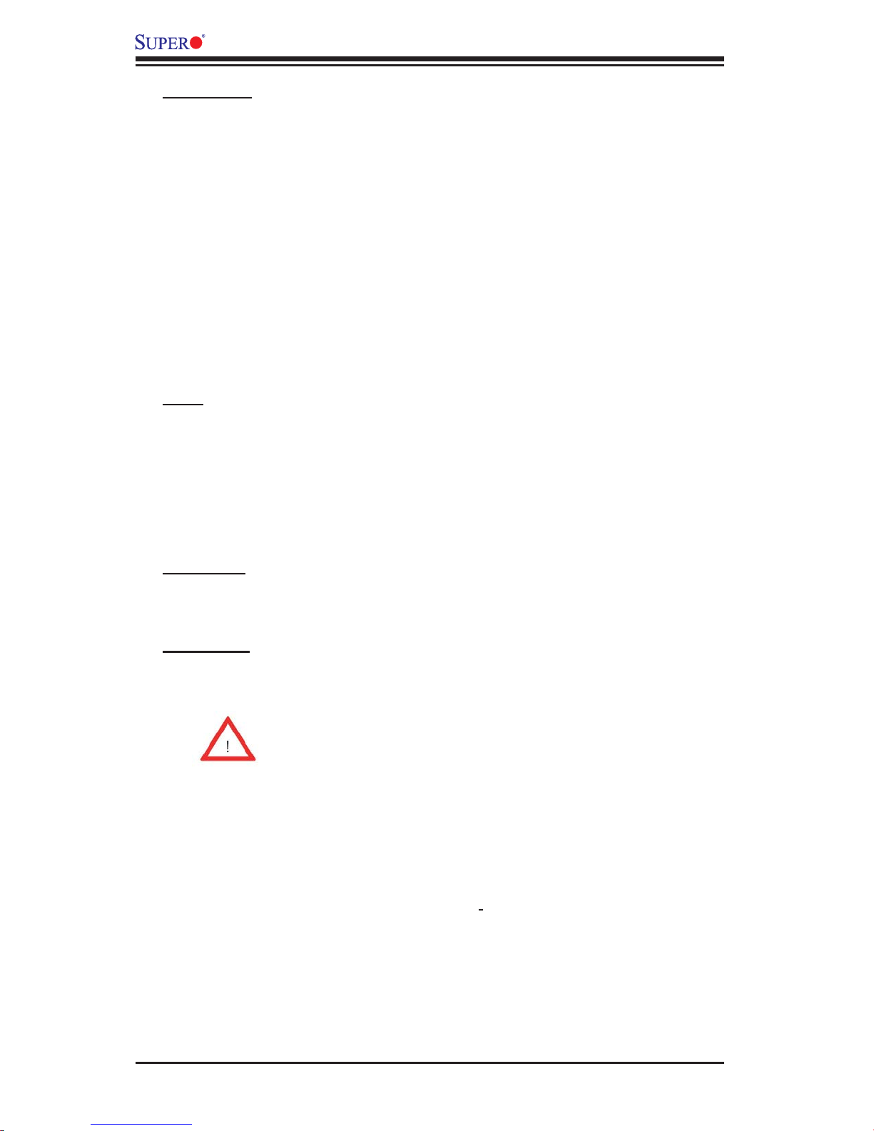
1. Press the socket lever to release
the load plate, which covers the CPU
socket, from its locking position.
2. Gently lift the socket lever to open
the load plate.
Socket Lever
Load Plate
Load Plate
2-2

3. Locate Pin 1 on the CPU socket. (Note:
Pin 1 is the corner marked with a triangle).
Please note that the North Key and the
South Key are located vertically in the
CPU housing.
4. Position the motherboard in such a way
that Pin 1 of the CPU socket is located at
the left bottom of the CPU housing.
5. Use your thumb and your index fi nger to
hold the CPU at the North Center Edge and
the South Center Edge of the CPU.
6. Align Pin 1 of the CPU with Pin 1 of the
socket. Once aligned, carefully lower the
CPU straight down to the socket. (**Do not
drop the CPU on the socket. Do not move
the CPU horizontally or vertically. Do not
rub the CPU against the surface or against
any pins of the socket to avoid damage to
the CPU or the socket.)
Chapter 2: Installation
North Key
Pin 1
South Key
North Center Edge
South Center Edge
7. With the CPU inside the socket, inspect
the four corners of the CPU to make sure
that the CPU is properly installed.
Socket Lever
8. Use your thumb to gently push the lever
down and lock it in the hook.
9. If the CPU is properly installed into the
socket, the plastic cap will be automatically
released from the load plate when the lever
is pushed into the hook. Remove the plastic
cap from the motherboard.
Plastic cap is released
from the load plate if
CPU properly installed.
CPU in the CPU socket
2-3
PDSLA/PDSLE User's Manual
Installation of the Heatsink
1. Locate the CPU Fan on the motherboard.
(Refer to the layout on Page 1-4 for the
CPU Fan location.)
2. Position the heatsink in such a way that
the heatsink fan wires are closest to the
CPU fan and are not interfered with other
component. 3. Inspect the CPU Fan wires
to make sure that the wires are routed
through the bottom of the heatsink.
4. Remove the thin layer of the protective
fi lm from the copper core of the heatsink.
(*Warning: CPU overheat may occur if the
protective fi lm is not removed from the
heatsink.)
5. Apply the proper amount of thermal
grease on the CPU. (*Note: if your heatsink
came with a thermal pad, please ignore
this step.)
6. If necessary, rearrange the wires to make
sure that the wires are not pinched between
the heatsink and the CPU. Also make sure
to keep clearance between the fan wires
and the fi ns of the heatsink.
7. Align the four heatsink fasteners with the
mounting holes on the motherboard. Gently
push the fasteners into the mounting holes
until you hear a "click".
8. Repeat Step 6 to insert all four heatsink
fasteners into the mounting holes.
Thermal Grease
CPU
Fan Wires
Heatsink Fins
9. Once all four fasteners are securely
inserted into the mounting holes and the
heatsink is properly installed on the moth-
erboard, connect the heatsink fan wires to
the CPU Fan connector.
Heatsink Fas-
tener
2-4
Heatsink Removal
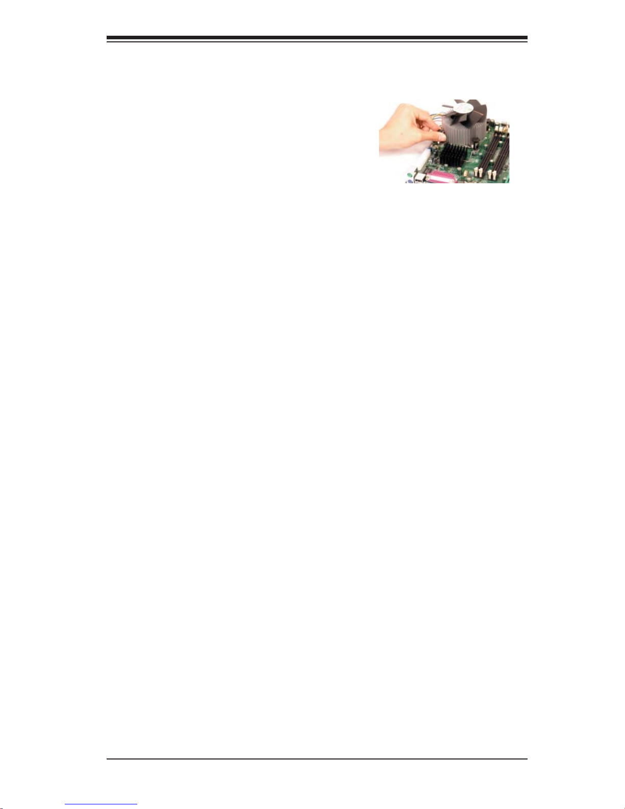
1. Unplug the power cord from the power
supply.
2. Disconnect the heatsink fan wires from the
CPU fan header.
3. Use your fi nger tips to gently press on the
fastener cap and rotate counterclockwise to
make a 1/4 (90
4. Repeat Step 3 to loosen all fasteners from
the mounting holes.
5. With all fasteners loosened, remove the
heatsink from the CPU.
0
) turn.
Chapter 2: Installation
2-3 Mounting the Motherboard in the Chassis
All motherboards have standard mounting holes to fi t different types of chassis.
Make sure that the locations of all the mounting holes for both the motherboard
and the chassis match. Although a chassis may have both plastic and metal
mounting fasteners, metal ones are highly recommended because they ground the
motherboard to the chassis. Make sure the metal standoffs click in or are screwed
in tightly. Then use a screwdriver to secure the motherboard onto the motherboard
tray. Since some components are located very close to the mounting holes, please
take precautionary measures needed to prevent the components from being dam-
aged when you install the motherboard into the chassis.
Note: some components are very close to the mounting holes, please take all
precautionary measures to prevent damage done the these components when
mounting the motherboard to the chassis.
2-5
PDSLA/PDSLE User's Manual
2-4 Installing DDR2 Memory
CAUTION
Exercise extreme care when installing or removing memory modules
to prevent any possible damage.
Memory Module Installation
1. Insert each DDR2 memory module vertically into its slot. Pay attention to the
notch along the bottom of the module to prevent inserting the module incor-
rectly. (See support information below.)
2. Gently press down on the memory module until it snaps into place.
Support
The PDSLA/PDSLE supports Single/Dual channel, unbuffered, non-ECC,
DDR2 667/533/400 SDRAM. Populating DIMM#1A,DIMM#1B, and/or
DIMM#2A, DIMM#2B with memory modules of the same size and the same
type will result in dual channel, two-way interleaved memory which is faster
than single channel, non-interleaved memory.
Note: Due to memory allocation to system devices, memory remaining available
for operational use will be reduced when 4 GB of RAM is used. The reduction in
memory availability is disproportional. (Refer to the Memory Availability Table below
for details.
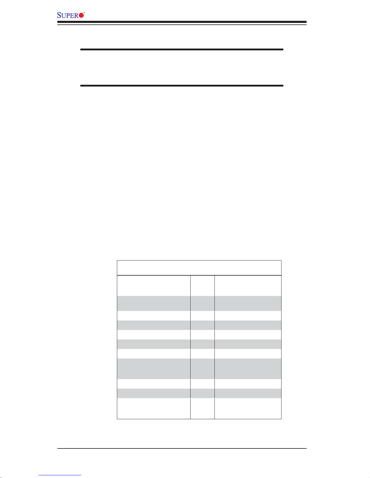
Possible System Memory Allocation & Availability
System Device Size Physical Memory
Firmware Hub fl ash memory
(System BIOS)
Local APIC 4 KB 3.99
Area Reserved for the chipset 2 MB 3.99
I/O APIC (4 Kbytes) 4 KB 3.99
PCI Enumeration Area 1 256 MB 3.76
PCI Express (256 MB) 256 MB 3.51
PCI Enumeration Area 2 (if
needed) -Aligned on 256-MB
boundary-
VGA Memory 16 MB 2.85
TSEG 1 MB 2.84
Memory available to System &
OS applications
1 MB 3.99
512 MB 3.01
Remaining (-Available)
(4 GB Total System Memory)
2.84
2-6
 Loading...