

Page 1

M11SDV-4C-LN4F
M11SDV-4CT-LN4F
M11SDV-8C-LN4F
M11SDV-8CT-LN4F
M11SDV-8C+-LN4F
USER MANUAL
Revision 1.0a
Page 2

The information in this user’s manual has been carefully reviewed and is believed to be accurate. The vendor assumes
!
no responsibility for any inaccuracies that may be contained in this document, and makes no commitment to update
or to keep current the information in this manual, or to notify any person or organization of the updates. Please Note:
For the most up-to-date version of this manual, please see our website at www.supermicro.com.
Super Micro Computer, Inc. ("Supermicro") reserves the right to make changes to the product described in this manual
at any time and without notice. This product, including software and documentation, is the property of Supermicro and/
or its licensors, and is supplied only under a license. Any use or reproduction of this product is not allowed, except
as expressly permitted by the terms of said license.
IN NO EVENT WILL Super Micro Computer, Inc. BE LIABLE FOR DIRECT, INDIRECT, SPECIAL, INCIDENTAL,
SPECULATIVE OR CONSEQUENTIAL DAMAGES ARISING FROM THE USE OR INABILITY TO USE THIS PRODUCT
OR DOCUMENTATION, EVEN IF ADVISED OF THE POSSIBILITY OF SUCH DAMAGES. IN PARTICULAR, SUPER
MICRO COMPUTER, INC. SHALL NOT HAVE LIABILITY FOR ANY HARDWARE, SOFTWARE, OR DATA STORED
OR USED WITH THE PRODUCT, INCLUDING THE COSTS OF REPAIRING, REPLACING, INTEGRATING,
INSTALLING OR RECOVERING SUCH HARDWARE, SOFTWARE, OR DATA.
Any disputes arising between manufacturer and customer shall be governed by the laws of Santa Clara County in the
State of California, USA. The State of California, County of Santa Clara shall be the exclusive venue for the resolution
of any such disputes. Supermicro's total liability for all claims will not exceed the price paid for the hardware product.
FCC Statement: This equipment has been tested and found to comply with the limits for a Class B digital device
pursuant to Part 15 of the FCC Rules. These limits are designed to provide reasonable protection against harmful
interference when the equipment is operated in a commercial environment. This equipment generates, uses, and can
radiate radio frequency energy and, if not installed and used in accordance with the manufacturer’s instruction manual,
may cause harmful interference with radio communications. Operation of this equipment in a residential area is likely
to cause harmful interference, in which case you will be required to correct the interference at your own expense.
California Best Management Practices Regulations for Perchlorate Materials: This Perchlorate warning applies only
to products containing CR (Manganese Dioxide) Lithium coin cells. “Perchlorate Material-special handling may apply.
See www.dtsc.ca.gov/hazardouswaste/perchlorate.
WARNING: This product can expose you to chemicals including
lead, known to the State of California to cause cancer and birth
defects or other reproductive harm. For more information, go
to www.P65Warnings.ca.gov.
The products sold by Supermicro are not intended for and will not be used in life support systems, medical equipment,
nuclear facilities or systems, aircraft, aircraft devices, aircraft/emergency communication devices or other critical
systems whose failure to perform be reasonably expected to result in signicant injury or loss of life or catastrophic
property damage. Accordingly, Supermicro disclaims any and all liability, and should buyer use or sell such products
for use in such ultra-hazardous applications, it does so entirely at its own risk. Furthermore, buyer agrees to fully
indemnify, defend and hold Supermicro harmless for and against any and all claims, demands, actions, litigation, and
proceedings of any kind arising out of or related to such ultra-hazardous use or sale.
Manual Revision 1.0a
Release Date: February 25, 2019
Unless you request and receive written permission from Super Micro Computer, Inc., you may not copy any part of this
document. Information in this document is subject to change without notice. Other products and companies referred
to herein are trademarks or registered trademarks of their respective companies or mark holders.
Copyright © 2019 by Super Micro Computer, Inc.
All rights reserved.
Printed in the United States of America
Page 3

Preface
Preface
About This Manual
This manual is written for system integrators, IT technicians and knowledgeable end users. It
provides information for the installation and use of the M11SDV-4C/4CT/8C/8CT/8C+-LN4F
motherboard.
About This Motherboard
The Supermicro M11SDV-4C/4CT/8C/8CT/8C+-LN4F motherboard supports an AMD EPYC™
3000 SoC series processor with up to 8 cores and 16 threads per socket. The AMD EPYC™
3000 upholds optimized performance with NVMe storage, offering up to 512GB of memory,
with speeds of up to 2666MHz. It offers an Intelligent Platform Management Interface (IPMI)
feature, IPMI out-of-band, and a power usage effectiveness mode that provides management
and monitoring capabilities, as well as a M.2 solid-state drive. This is a high performance,
low powered mini-ITX motherboard that is ideal for super compact servers requiring high
compute power. Please note that this motherboard is intended to be installed and serviced
by professional technicians only. For processor/memory updates, please refer to our website
at http://www.supermicro.com/products/.
Manual Organization
Chapter 1 describes the features, specications and performance of the motherboard, and
provides detailed information on the AMD® EPYC 3000 SoC.
Chapter 2 provides hardware installation instructions. Read this chapter when installing the
processor, memory modules, and other hardware components into the system.
If you encounter any problems, see Chapter 3, which describes troubleshooting procedures
for video, memory, and system setup stored in the CMOS.
Chapter 4 includes an introduction to the BIOS, and provides detailed information on running
the BIOS Setup utility.
Appendix A provides BIOS Error Beep Codes.
Appendix B lists software program installation instructions.
Appendix C lists standardized warning statements in various languages.
Appendix D provides UEFI BIOS Recovery instructions.
3
Page 4

Super M11SDV-4C/4CT/8C/8CT/8C+-LN4F User's Manual
Contacting Supermicro
Headquarters
Address: Super Micro Computer, Inc.
980 Rock Ave.
San Jose, CA 95131 U.S.A.
Tel: +1 (408) 503-8000
Fax: +1 (408) 503-8008
Email: marketing@supermicro.com (General Information)
support@supermicro.com (Technical Support)
Website: www.supermicro.com
Europe
Address: Super Micro Computer B.V.
Het Sterrenbeeld 28, 5215 ML
's-Hertogenbosch, The Netherlands
Tel: +31 (0) 73-6400390
Fax: +31 (0) 73-6416525
Email: sales@supermicro.nl (General Information)
support@supermicro.nl (Technical Support)
rma@supermicro.nl (Customer Support)
Website: www.supermicro.nl
Asia-Pacic
Address: Super Micro Computer, Inc.
3F, No. 150, Jian 1st Rd.
Zhonghe Dist., New Taipei City 235
Taiwan (R.O.C)
Tel: +886-(2) 8226-3990
Fax: +886-(2) 8226-3992
Email: support@supermicro.com.tw
Website: www.supermicro.com.tw
4
Page 5

Preface
Table of Contents
Chapter 1 Introduction
1.1 Checklist ...............................................................................................................................8
Quick Reference ...............................................................................................................13
Quick Reference Table ......................................................................................................15
Motherboard Features .......................................................................................................16
1.2 Processor Overview ...........................................................................................................19
1.3 Special Features ................................................................................................................19
Recovery from AC Power Loss .........................................................................................19
1.4 System Health Monitoring ..................................................................................................20
Onboard Voltage Monitors ................................................................................................20
Fan Status Monitor with Firmware Control .......................................................................20
Environmental Temperature Control .................................................................................20
System Resource Alert......................................................................................................20
1.5 ACPI Features ....................................................................................................................21
1.6 Power Supply .....................................................................................................................21
Chapter 2 Installation
2.1 Static-Sensitive Devices .....................................................................................................22
Precautions .......................................................................................................................22
Unpacking .........................................................................................................................22
2.2 Motherboard Installation .....................................................................................................23
Tools Needed ....................................................................................................................23
Location of Mounting Holes ..............................................................................................23
Installing the Motherboard.................................................................................................24
2.3 Memory Support and Population ........................................................................................25
Memory Support ................................................................................................................25
DIMM Module Population Conguration ...........................................................................26
DIMM Module Population Sequence ................................................................................27
DIMM Installation ..............................................................................................................28
DIMM Removal .................................................................................................................28
2.4 Rear I/O Ports ....................................................................................................................29
2.5 Front Control Panel ............................................................................................................33
5
Page 6

Super M11SDV-4C/4CT/8C/8CT/8C+-LN4F User's Manual
2.6 Connectors and Headers ...................................................................................................38
Power Connections ...........................................................................................................38
Headers ..............................................................................................................................39
2.7 Jumper Settings .................................................................................................................46
How Jumpers Work ...........................................................................................................46
2.8 LED Indicators ....................................................................................................................52
Chapter 3 Troubleshooting
3.1 Troubleshooting Procedures ..............................................................................................55
Before Power On ..............................................................................................................55
No Power ..........................................................................................................................55
No Video ...........................................................................................................................55
System Boot Failure ..........................................................................................................56
Memory Errors ..................................................................................................................56
Losing the System's Setup Conguration .........................................................................57
When the System Becomes Unstable ..............................................................................57
3.2 Technical Support Procedures ...........................................................................................59
3.3 Frequently Asked Questions ..............................................................................................60
3.4 Battery Removal and Installation .......................................................................................61
Battery Removal ................................................................................................................61
Proper Battery Disposal ....................................................................................................61
Battery Installation .............................................................................................................61
3.5 Returning Merchandise for Service ....................................................................................62
Chapter 4 UEFI BIOS
4.1 Introduction .........................................................................................................................63
Starting the Setup Utility ...................................................................................................63
4.2 Main Setup .........................................................................................................................64
4.3 Advanced ............................................................................................................................66
4.4 IPMI ....................................................................................................................................84
4.5 Event Logs .........................................................................................................................88
4.6 Security ...............................................................................................................................90
4.7 Boot ....................................................................................................................................95
4.8 Save & Exit .........................................................................................................................97
6
Page 7

Appendix A BIOS Codes
Appendix B Software Installation
B.1 Installing Software Programs ...........................................................................................101
B.2 SuperDoctor® 5 ................................................................................................................102
Appendix C Standardized Warning Statements
Battery Handling ..............................................................................................................103
Product Disposal .............................................................................................................105
Appendix D UEFI BIOS Recovery
7
Page 8

Super M11SDV-4C/4CT/8C/8CT/8C+-LN4F User's Manual
Chapter 1
Introduction
Congratulations on purchasing your computer motherboard from an acknowledged leader in
the industry. Supermicro boards are designed with the utmost attention to detail to provide
you with the highest standards in quality and performance.
Please check that the following items have all been included with your motherboard. If
anything listed here is damaged or missing, contact your retailer. The following items are
included in the retail box:
1.1 Checklist
Main Parts List (included in the retail box)
Description Part Number Quantity
Supermicro Motherboard M11SDV-4C/4CT/8C/8CT/8C+-LN4F 1
Quick Reference Guide MNL-2172-QRG 1
SATA Data Cables CBL-0044L 4
SATA Power Cable CBL-PWEX-0982 1
24-pin ATX to 4-pin Power Cable CBL-PWEX-1063 1
I/O Shield MCP-260-00084-0N 1
Main Parts List (included in the Bulk box)
Description Part Number Quantity
Supermicro Motherboard M11SDV-4C/4CT/8C/8CT/8C+-LN4F 1
SATA Data Cables CBL-0044L 2
SATA Power Cable CBL-PWEX-0982 1
24-pin ATX to 4-pin Power Cable CBL-PWEX-1063 1
I/O Shield MCP-260-00084-0N 1
8
Page 9

Chapter 1: Introduction
Important Links
For your system to work properly, please follow the links below to download all necessary
drivers/utilities and the user’s manual for your server.
• Supermicro product manuals: http://www.supermicro.com/support/manuals/
• Product drivers and utilities: https://www.supermicro.com/wftp/driver/
• Product safety info: http://www.supermicro.com/about/policies/safety_information.cfm
• If you have any questions, please contact our support team at: support@supermicro.com
This manual may be periodically updated without notice. Please check the Supermicro website
for possible updates to the manual revision level.
9
Page 10
Super M11SDV-4C/4CT/8C/8CT/8C+-LN4F User's Manual
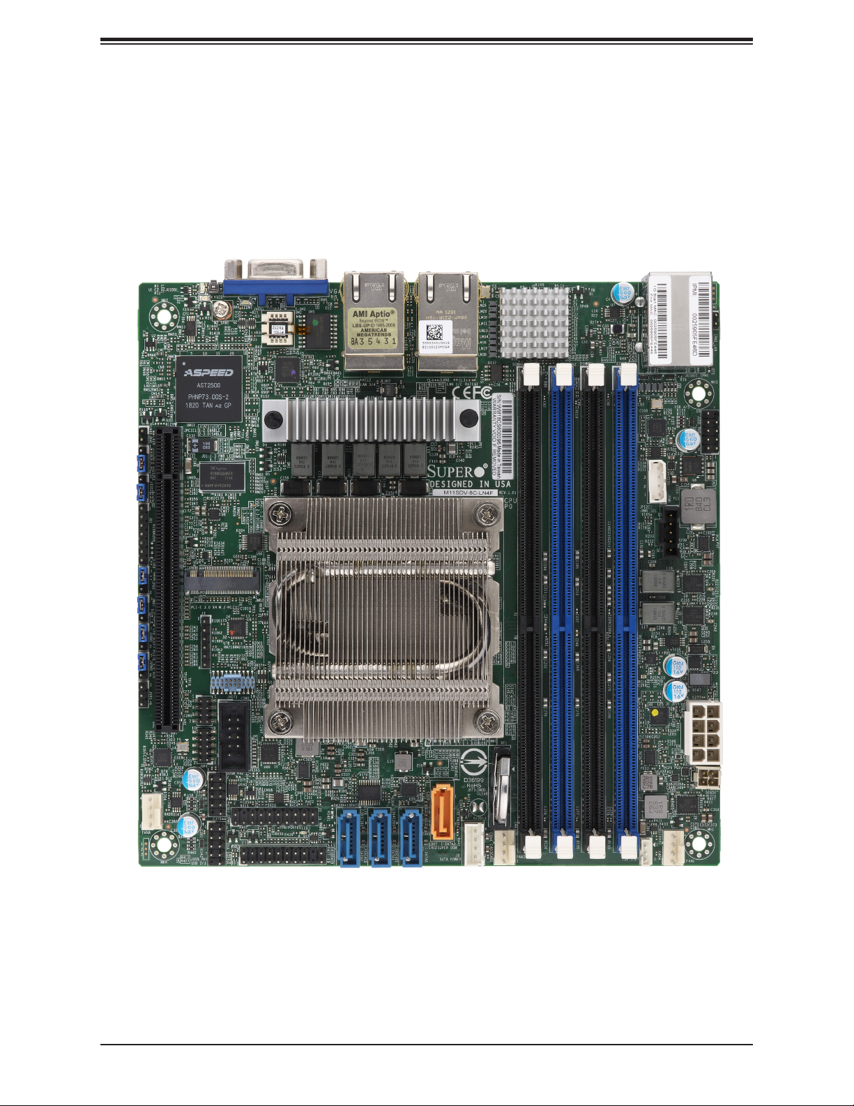
Figure 1-1. M11SDV-4C/4CT/8C/8CT-LN4F Motherboard Image
10
Page 11
Chapter 1: Introduction
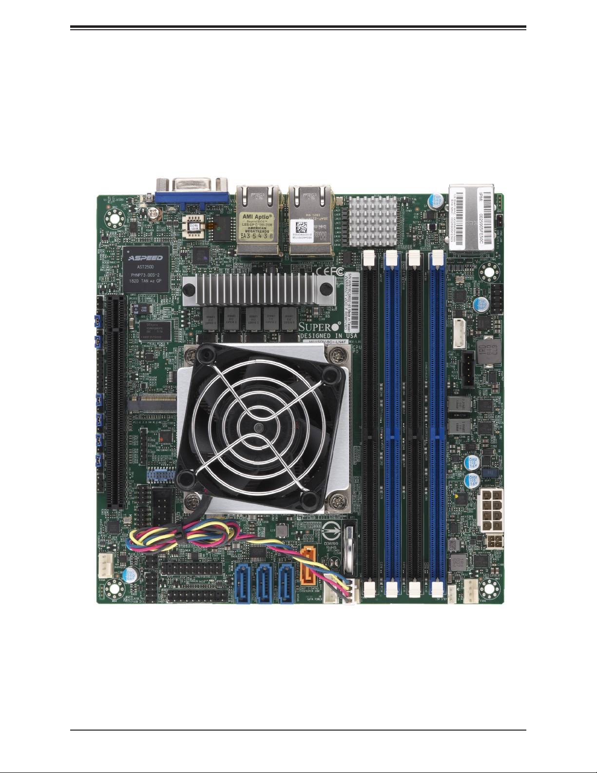
Figure 1-2. M11SDV-8C+-LN4F Motherboard Image
11
Page 12
Super M11SDV-4C/4CT/8C/8CT/8C+-LN4F User's Manual
JBM1
JI2C1
JI2C2
JD1
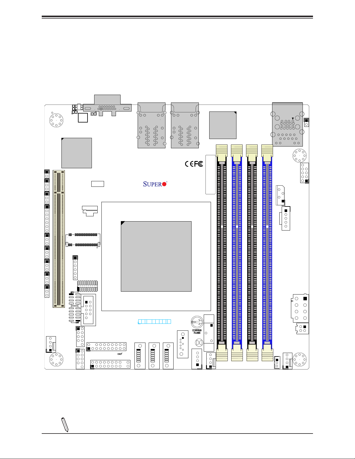
Figure 1-3. M11SDV-4C/4CT/8C/8CT/8C+-LN4F Motherboard Layout
(not drawn to scale)
VGA
LED1
UID
LED2
AST2500
JPCIE1
CPU SLOT7 PCI-E 3.0 X16
BMC
1-3:PWR LEDJD1:
4-7:SPEAKER
M2_SRW1
JPG1:
VGA
JWD1:WATCH DOG
LEDM1
1-2:ENABLE
2-3:DISABLE
1-2:RST
2-3:NMI
JI2C1/JI2C2:
1-2:ENABLE
2-3:DISABLE
LAN 3/4
M11SDV-4CT-LN4F
DESIGNED IN USA
REV:1.01A
LAN 1/2
i350
BAR CODE
1
IPMI_LAN
USB 6/7(3.0)
JSMB
JBM2
USB 4/5
JPI2C1
JWD1
JVRM1
JVRM2
JVR1
FANA
JPG1
SGPIO1
JGP1
USB 0/1
USB 2/3
JMD2
PCI-E 3.0 X4 M.2-HC
J1
JHDT1
COM1
JTPM1
DIMMB2
DIMMA2
DIMMB1
CPU
BT1
NIC
NIC HDD
PWR
OH/FF
PWR
RST
X
UID
ON
JF1
SATA2
LED3
JF1
X
NMI
1
2
LED
LED
SATA0
SATA1
SATA3
SUPER DOM
SATA POWER
JBT1
J6
FAN2
DIMMA1
JPV1
PJ1
FAN1
JSTBY1
Note: Components not documented are for internal testing only.
12
Page 13
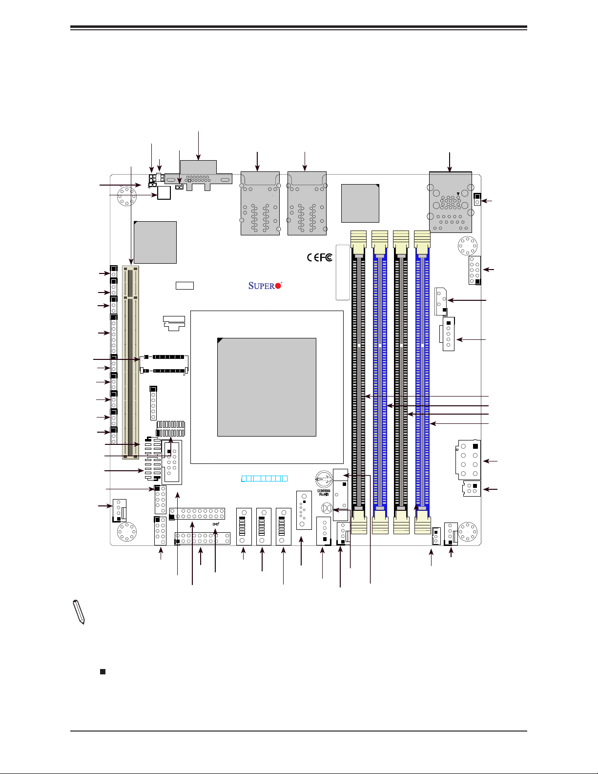
Quick Reference
Chapter 1: Introduction
LED2
M2_SRW1
JBM1
JI2C1
JI2C2
JD1
JMD2
JPG1
JWD1
JVRM1
JVRM2
JVR1
SGPIO1
JHDT1
JGP1
USB0/1
FANA
JPCIE1
JBM1
JI2C1
JI2C2
JD1
JPG1
JWD1
JVRM1
JVRM2
JVR1
FANA
LED1
UID
LED1
UID
LED2
M2_SRW1
BMC
AST2500
1-3:PWR LEDJD1:
4-7:SPEAKER
JPCIE1
CPU SLOT7 PCI-E 3.0 X16
JPG1:
VGA
JWD1:WATCH DOG
JMD2
PCI-E 3.0 X4 M.2-HC
J1
SGPIO1
JGP1
USB 0/1
USB 2/3
LEDM1
LEDM1
JI2C1/JI2C2:
1-2:ENABLE
2-3:DISABLE
1-2:ENABLE
2-3:DISABLE
1-2:RST
2-3:NMI
JHDT1
COM1
VGA
VGA
JTPM1
IPMI_LAN
LAN3/4
LAN 3/4
M11SDV-4CT-LN4F
DESIGNED IN USA
REV:1.01A
LAN1/2
LAN 1/2
i350
BAR CODE
1
USB6/7 (3.1 Gen 1)
IPMI_LAN
USB 6/7(3.0)
USB 4/5
JSMB
JPI2C1
JBM2
JBM2
USB4/5
JSMB
JPI2C1
DIMMB2
DIMMA2
DIMMB1
CPU
DIMMA1
DIMMA1
DIMMA2
DIMMB1
DIMMB2
JPV1
BT1
NIC
NIC HDD
PWR
OH/FF
PWR
RST
X
X
NMI
1
UID
2
LED
ON
JF1
LED3
JF1
LED
SATA2
SATA3
SUPER DOM
SATA POWER
JBT1
J6
FAN2
JSTBY1
SATA0
SATA1
PJ1
FAN1
JPV1
PJ1
USB2/3
COM1
JF1
JTPM1
LED3
SATA 2
SATA 1
SATA 0
SATA 3
J6
JBT1
FAN2
BT1
FAN1
JSTBY1
Notes:
• See Chapter 2 for detailed information on jumpers, I/O ports, and JF1 front panel connec-
tions. Jumpers/LED indicators not indicated are used for testing only.
• " " indicates the location of Pin 1.
• When LED3 (Onboard Power LED indicator) is on, system power is on. Unplug the power
cable before installing or removing any components.
13
Page 14
Super M11SDV-4C/4CT/8C/8CT/8C+-LN4F User's Manual
Figure 1-4. X11SDV-TP8F Series Motherboard Model Variation Table
Model CPU Core Threads TDP(W)
M11SDV-8C+-LN4F 3251 8 16 50 2.5 3.1 16 2666 active
M11SDV-8C-LN4F 3251 8 16 50 2.5 3.1 16 2666 passive
M11SDV-8CT-LN4F 3201 8 8 30 1.5 3.1 16 2133 passive
M11SDV-4C-LN4F 3151 4 8 45 2.7 2.9 16 2666 passive
M11SDV-4CT-LN4F 3101 4 4 35 2.1 2.0 8 2666 passive
Base
Freq
(GHz)
Boost
Freq
(GHz)
L3 (MB)
DDR
Freq
Heatsink
14
Page 15

Chapter 1: Introduction
Quick Reference Table
Jumper Description Default Setting
JBM1 Disable Share LAN Pin 1-2 Open (Enable)
JBM2 Disable IPMI/Share LAN Pin 1-2 Open (Enable)
JBT1 CMOS Clear Open: Normal, Closed: Clear CMOS
JI2C1, JI2C2 SMB to PCI-E Slots Enable/Disable Pins 2-3 (Disabled)
JPG1 Onboard VGA Enable/Disable Pins 1-2 (Enabled)
JVRM1 VRM SMB Clock (to BMC or PCH) Pins 1-2 (Normal)
JVRM2 VRM SMB Data (to BMC or PCH) Pins 1-2 (Normal)
JWD1 Watch Dog Timer Pins 1-2 (Reset)
LED Description Status
LED1 UID LED Solid Blue: Unit Identied
LED2 Overheat (OH)/PWR Fail/Fan Fail LED
LED3 Power LED Solid Green: Power On
LEDM1 BMC Heartbeat Blinking Green: BMC Normal
Solid Red: Overheat
Blinking Red: PWR Fail or Fan Fail
Connector Description
BT1 Onboard Battery
COM1 RS232 COM Port Header
FAN1 - FAN2, FANA CPU/System Fan Headers
IPMI_LAN Dedicated IPMI LAN Port
JD1 Pins 1-2: PWR LED, Pin 4-7: Speaker
JF1 Front Control Panel Header
JGP1 8-bit General Purpose I/O Header
JMD2 M.2 Slot 2280 M-key (PCIe x 4/SATA 3.0)
JPCIE1 PCI-E 3.0 x 16 Slot
JPI2C1 Power I2C System Management Bus (Power SMB) Header
JPV1 8-pin 12V DC Power Input (Required for 12V only or 24-pin ATX power)
JSMB System Management Bus Header
JSTBY1 Standby Power Connector
JTPM1 Trusted Platform Module (TPM)/Port 80 Connector
LAN1 - LAN4 1 GbE LAN (RJ45) Ports
PJ1 Header for ATX Power Signal 5VSTBY/Power ON/Power Good/Ground; 24pin ATX to
4pin power cable for PJ1 (Supermicro P/N: CBL-PWEX-1063)
SATA0 - SATA3 SATA 3.0 Ports
UID Unit Identier Switch
USB0-5 USB 2.0 Header
USB6/7 Back Panel USB 3.0 Ports
VGA VGA Port (back panel)
15
Page 16
Super M11SDV-4C/4CT/8C/8CT/8C+-LN4F User's Manual
Motherboard Features
Motherboard Features
CPU
• Supports an AMD EPYC™ 3000 SoC processor
Memory
• Supports DDR4 ECC/Non-ECC RDIMM, UDIMM, and LRDIMM memory in 4 DIMM slots, up to 512GB, with speed of up
to 2666MHz.
Note: When the motherboard is populated with 4 modules of 2S4R/4DR DDR4 LRDIMM, the memory will operate
at speed of 2133MHz.
When the motherboard is fully populated with 4 modules of single rank DDR4 RDIMM, the memory will operate at
speed of 2133MHz.
When the motherboard is fully populated with 4 modules of 2R/2DR/2S2R/2S4R DDR4 RDIMM, the memory will
operate at speed of 1866MHz.
When the motherboard is fully populated with 4 modules of single rank DDR4 UDIMM, the memory will operate at
speed of 2133MHz.
When the motherboard is fully populated with 4 modules of 2R/2DR DDR4 UDIMM, the memory will operate at
speed of 1866MHz.
DIMM Size
• 4GB, 8GB, 16GB, 32GB, 64GB, and 128GB
Expansion Slots
• One (1) PCI-E 3.0 x 16 slot
Network Controller
• ASpeed AST2500 and Intel i350
Baseboard Management Controller (BMC)
• ASpeed AST2500
Graphics
• Graphics controller via ASpeed AST2500
I/O Devices
• Com Header • One (1) RS232 COM Port Header
• SATA 3.0 • Four (4) SATA 3.0 ports
Peripheral Devices
• Six (6) USB 2.0 ports in three (3) internal headers (USB0/1, USB2/3, USB4/5)
• Two (2) USB 3.0 ports on the I/O back panel (USB6/7)
Note: The table above is continued on the next page.
16
Page 17

Chapter 1: Introduction
Motherboard Features
BIOS
• 128Mb AMI BIOS® SPI Flash BIOS
• UEFI 2.6, ACPI 6.1, PCI FAV 3.0, SMBIOS 3.1, SPI dual/quad speed support, Real Time Clock (RTC) wakeup
Power Management
• ACPI power management
• Wake-On-LAN (JWOL)
• S5
• Power button override mechanism
• Power-on mode for AC power recovery
System Health Monitoring
• Onboard voltage monitors for Vcore, Vmem, Vsocrun, Vsocdual, +3.3V, +5V, +12V, +3.3V Stby, +5V Stby, VBAT, CPU
Temperature, System Temperature, Memory Temperature, Peripheral Temperature, and VRM Temperature
• CPU/System overheat control
• CPU Thermal Trip support
Fan Control
• Fan status monitoring with rmware
• Three (3) 4-pin fan headers with speed control
System Management
• IPMIVIEW, SMCIPMITOOL, IPMICFG
• System management via SuperDoctor® 5, Watch Dog
• Power supply monitoring
• SUM-INBand, SUM-OOB
LED Indicators
• CPU/system overheat LED
• Fan failed LED
• LAN activity LED
• UID LED
• Power LED
Other
• RoHS
Dimensions
• Mini-ITX form factor (6.75" x 6.75") (170 mm x 170 mm)
Note 1: For IPMI conguration instructions, please refer to the Embedded IPMI Conguration User's Guide available at http://www.supermicro.com/support/manuals/.
Note 2: If you purchase a Supermicro Out of Band (OOB) software license key
(Supermicro P/N: SFT-OOB--LIC), please DO NOT change the IPMI MAC address.
17
Page 18

Super M11SDV-4C/4CT/8C/8CT/8C+-LN4F User's Manual
Figure 1-5.
Chipset Block Diagram
3 Phase VR
Slot 1 PCIe x16 ( or 2 x 8 )
RJ45 x4
I350 PCIe x4
M.2_M PCIe x4
4 X SATA-III
Rear USB 3.0 x 2
Header USB 2.0 x 2
SVID
PCIe3.0_x16
8.0GT/s
Group B 0~15
PCIe3.0_x4
8.0GT/s
PCIe3.0_x4 / SATA x 1
8.0GT/s or 6Gb/s
SATA-III
6Gb/s
USB3.0
5Gbps
USB2.0
500Mbps
SVI2
Group A 12~15
Group A 0~3
USB_1_SS_0 & USB_1_HSD0
USB_1_SS_1 & USB_1_HSD1
MEM_DIMMA
Group A 4~7
AMD
BGA
RJ45
MEM_DIMMC
MEM_DIMMDMEM_DIMMB
2666MHz2666MHz
USB_0_HSD1
HUB
Header
USB2 x2
Header
USB2 x2
CPU1
HUB
USB_0_HSD0
PCIe x 1
LPC
TPM1.2 Header
Dedicated LAN
+
USB3.0
Note: This is a general block diagram and may not exactly represent the features on
your motherboard. See the previous pages for the actual specications of your motherboard.
REAR IO
VGA (KVM)
COM1 (Header)
Health Info.
1G LAN1G LAN
VGA
AST2500
SPI
FLASH
SPI 128Mb
18
Page 19

Chapter 1: Introduction
1.2 Processor Overview
The Supermicro M11SDV-4C/4CT/8C/8CT/8C+-LN4F motherboard supports an AMD EPYC™
3000 SoC series processor with up to 8 cores and 16 threads per socket. The AMD EPYC™
3000 upholds optimized performance with NVMe storage, offering up to 512GB of memory,
with speed of up to 2666MHz and 50W of power, while offering performance, reliability,
and high intelligence. It offers an Intelligent Platform Management Interface (IPMI) feature,
IPMI out-of-band, and a power usage effectiveness mode that provides management and
monitoring capabilities, as well as a M.2 solid-state drive. As a low-power system-on-a-chip
(SoC) motherboard, the M11SDV-4C/4CT/8C/8CT/8C+-LN4F is optimized for a variety of
workloads that requires high compute power in a compact form-factor.
The AMD EPYC™ 3000 supports the following features:
• Zen Microarchitecture, 14nm, System on Chip, RAS, Secure Memory Encryption (SME),
and Secure Encrypted Virtualization (SEV) for securely isolating hypervisors and virtual
machines VMS
• 16MB L3 Cache, up to 8 Core and 16 Thread
• ACPI Power Management Rev. 6.1
• Adaptive Thermal Management/Monitoring
• PCI-E 3.0, SATA 3.0, NVMe
1.3 Special Features
This section describes the health monitoring features of the
M11SDV-4C/4CT/8C/8CT/8C+-LN4F motherboard. The motherboard has an onboard
System Hardware Monitor chip AST2500 that supports system health monitoring.
Recovery from AC Power Loss
The Basic Input/Ouput System (BIOS) provides a setting that determines how the system
will respond when AC power is lost and then restored to the system. You can choose for the
system to remain powered off (in which case you must press the power switch to turn it back
on), or for it to automatically return to the power-on state. See the Advanced BIOS Setup
section for this setting. The default setting is Last State.
19
Page 20
Super M11SDV-4C/4CT/8C/8CT/8C+-LN4F User's Manual
1.4 System Health Monitoring
This section describes the health monitoring features of the M11SDV-4C/4CT/8C/8CT/8C+-LN4F
motherboard. The motherboard has an onboard Baseboard Management Controller (BMC)
chip that supports system health monitoring.
Onboard Voltage Monitors
The onboard voltage monitor will continuously scan crucial voltage levels. Once a voltage
becomes unstable, it will give a warning or send an error message to the screen. Users can
adjust the voltage thresholds to dene the sensitivity of the voltage monitor. Real time readings
of these voltage levels are all displayed in BIOS.
Fan Status Monitor with Firmware Control
The system health monitor chip can check the RPM status of a cooling fan. The CPU and
chassis fans are controlled by BIOS Thermal Management through the back panel. Refer
to the below table for available fan modes to choose the most appropriate one for nominal
operation.
Fan Mode Description
Full Speed Use this mode to set fan speed at full speed for maximum system cooling
Standard Use this mode to set fan speed for normal system cooling
Heavy I/O Use this mode to set fan speed for higher PCI-E add-on card area cooling
Optimal Use this mode to set fan speed for normal PCI-E add-on card area cooling
PUE2 Use this mode to set fan speed for best power efciency and maximum noise reduction
Environmental Temperature Control
System health sensors monitor temperatures and voltage settings of onboard processors
and the system in real time via the IPMI interface. Whenever the temperature of the CPU or
the system exceeds a user-dened threshold, system/CPU cooling fans will be turned on to
prevent the CPU or the system from overheating.
Note: To avoid possible system overheating, please provide adequate airow to your
system.
System Resource Alert
This feature is available when used with SuperDoctor 5® in the Windows OS or in the Linux
environment. SuperDoctor is used to notify the user of certain system events. For example,
you can congure SuperDoctor to provide you with warnings when the system temperature,
CPU temperatures, voltages and fan speeds go beyond a predened range.
20
Page 21

Chapter 1: Introduction
1.5 ACPI Features
ACPI stands for Advanced Conguration and Power Interface. The ACPI specication denes
a exible and abstract hardware interface that provides a standard way to integrate power
management features throughout a computer system, including its hardware, operating
system and application software. This enables the system to automatically turn on and off
peripherals such as CD-ROMs, network cards, hard disk drives and printers.
In addition to enabling operating system-directed power management, ACPI also provides a
generic system event mechanism for Plug and Play, and an operating system-independent
interface for conguration control. ACPI leverages the Plug and Play BIOS data structures,
while providing a processor architecture-independent implementation.
1.6 Power Supply
As with all computer products, a stable power source is necessary for proper and reliable
operation. It is even more important for processors that have high CPU clock rates.
It is strongly recommended that you use a high quality power supply that meets ATX power
supply Specication 2.02 or above. It must also be SSI compliant. (For more information,
please refer to the website at http://www.ssiforum.org/). Additionally, in areas where noisy
power transmission is present, you may choose to install a line lter to shield the computer
from noise. It is recommended that you also install a power surge protector to help avoid
problems caused by power surges.
Note: The M11SDV-4C/4CT/8C/8CT/8C+-LN4F motherboard supports either 12V DC in
power input or ATX power input. The 12V DC IN power input requires an 8-pin 12V DC
IN connection to the JPV1 header. ATX power input requires an 8-pin 12V connections
to JPV1 header and PJ1 a 4-pin power connector of an ATX power supply by power
cable (24-pin ATX to 4-pin power cable for PJ1, Supermicro P/N: CBL-PWEX-1063).
PJ1 allows motherboard control of the 5VStby, power on, power good, and ground
signals from the ATX power supply.
21
Page 22

Super M11SDV-4C/4CT/8C/8CT/8C+-LN4F User's Manual
Chapter 2
Installation
2.1 Static-Sensitive Devices
Electrostatic Discharge (ESD) can damage electronic com ponents. To prevent damage to your
motherboard, it is important to handle it very carefully. The following measures are generally
sufcient to protect your equipment from ESD.
Precautions
• Use a grounded wrist strap designed to prevent static discharge.
• Touch a grounded metal object before removing the board from the antistatic bag.
• Handle the board by its edges only; do not touch its components, peripheral chips, memory
modules or gold contacts.
• When handling chips or modules, avoid touching their pins.
• Put the motherboard and peripherals back into their antistatic bags when not in use.
• For grounding purposes, make sure your computer chassis provides excellent conductivity
between the power supply, the case, the mounting fasteners and the motherboard.
• Use only the correct type of onboard CMOS battery. Do not install the onboard battery
upside down to avoid possible explosion.
Unpacking
The motherboard is shipped in antistatic packaging to avoid static damage. When unpacking
the motherboard, make sure that the person handling it is static protected.
22
Page 23
Chapter 2: Installation
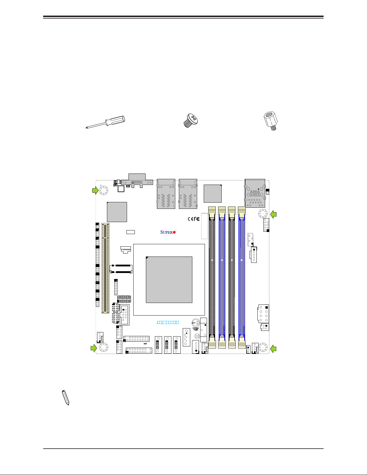
2.2 Motherboard Installation
All motherboards have standard mounting holes to t different types of chassis. Make sure
that the locations of all the mounting holes for both the motherboard and the chassis match.
Although a chassis may have both plastic and metal mounting fasteners, metal ones are
highly recommended because they ground the motherboard to the chassis. Make sure that
the metal standoffs click in or are screwed in tightly.
Phillips Screwdriver (1)
Tools Needed
LED1
UID
LED2
M2_SRW1
BMC
AST2500
JBM1
1-3:PWR LEDJD1:
JI2C1
4-7:SPEAKER
JI2C2
JPCIE1
CPU SLOT7 PCI-E 3.0 X16
JPG1:
VGA
SGPIO1
JMD2
PCI-E 3.0 X4 M.2-HC
J1
JWD1:WATCH DOG
JHDT1
JD1
JPG1
JWD1
JVRM1
JVRM2
JVR1
1-2:ENABLE
2-3:DISABLE
1-2:RST
2-3:NMI
LEDM1
JI2C1/JI2C2:
1-2:ENABLE
2-3:DISABLE
Phillips Screws (4)
Standoffs (4)
Only if Needed
VGA
LAN 3/4
M11SDV-4CT-LN4F
DESIGNED IN USA
REV:1.01A
CPU
i350
DIMMA1
IPMI_LAN
USB 6/7(3.0)
JSMB
DIMMA2
LAN 1/2
BAR CODE
1
DIMMB1
JBM2
USB 4/5
JPI2C1
DIMMB2
JPV1
SATA POWER
BT1
JBT1
J6
FAN2
JSTBY1
PJ1
FAN1
NIC
NIC HDD
PWR
OH/FF
PWR
RST
X
X
NMI
1
UID
2
LED
LED
JGP1
USB 0/1
USB 2/3
COM1
JTPM1
JF1
FANA
ON
JF1
SATA0
SATA1
SATA2
LED3
SATA3
SUPER DOM
Location of Mounting Holes
Note: 1) To avoid damaging the motherboard and its components, please do not use
a force greater than 8 lb/inch on each mounting screw during motherboard installation.
2) Some components are very close to the mounting holes. Please take precautionary
measures to avoid damaging these components when installing the motherboard to
the chassis.
23
Page 24

Super M11SDV-4C/4CT/8C/8CT/8C+-LN4F User's Manual
Installing the Motherboard
1. Locate the mounting holes on the motherboard. See the previous page for the location.
2. Locate the matching mounting holes on the chassis. Align the mounting holes on the
motherboard against the mounting holes on the chassis.
3. Install standoffs in the chassis as needed.
4. Install the motherboard into the chassis carefully to avoid damaging other motherboard
components.
5. Using the Phillips screwdriver, insert a Phillips head #6 screw into a mounting hole on
the motherboard and its matching mounting hole on the chassis.
6. Repeat Step 5 to insert #6 screws into all mounting holes.
7. Make sure that the motherboard is securely placed in the chassis.
Note: Images displayed are for illustration only. Your chassis or components might
look different from those shown in this manual.
24
Page 25

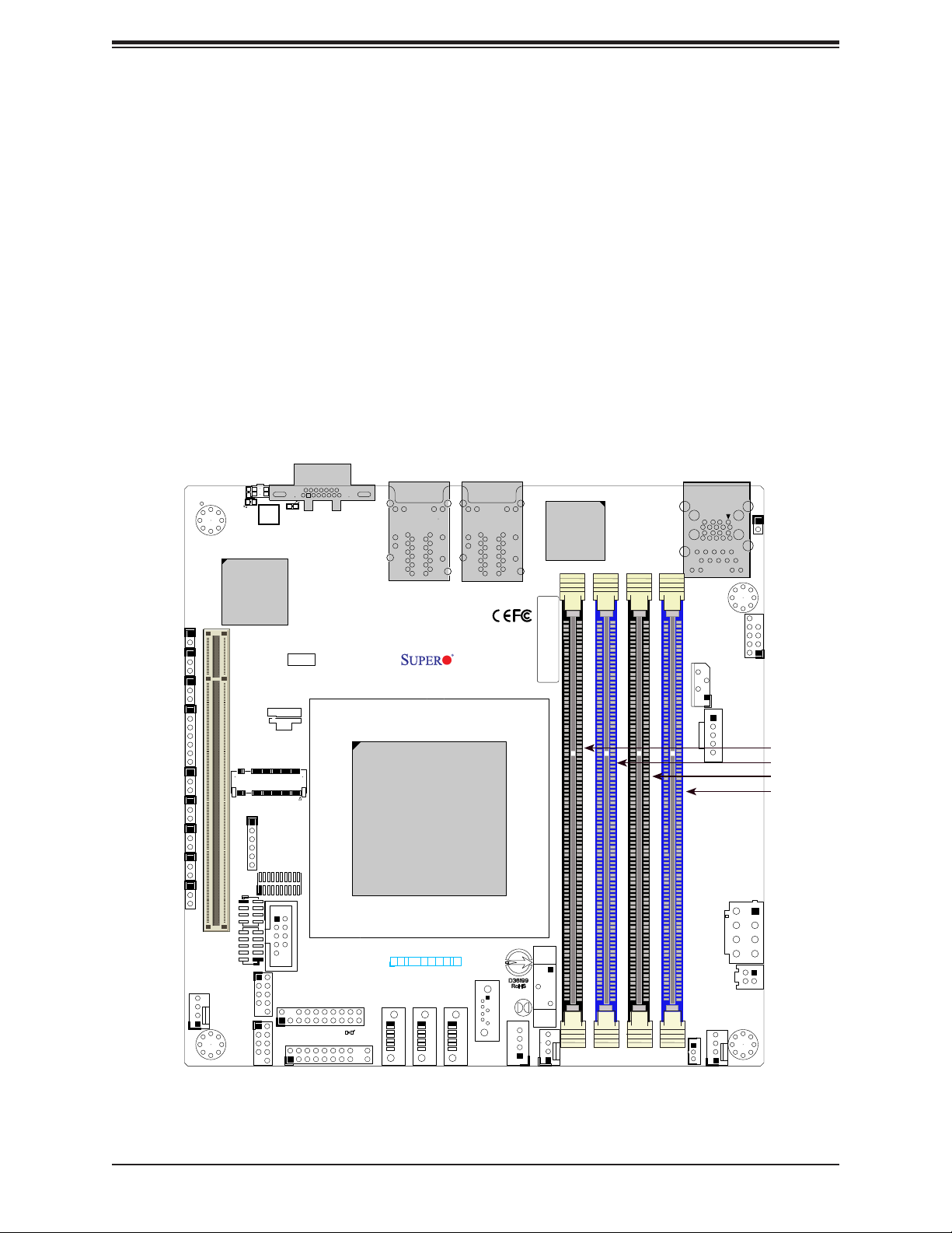
2.3 Memory Support and Population
Important: Exercise extreme care when installing or removing DIMM modules to pre-
vent any possible damage.
Note: When the motherboard is populated with 4 modules of 2S4R/4DR DDR4
LRDIMM, the memory speed will operate at 2133MHz.
When the motherboard is fully populated with 4 modules of single rank DDR4 RDIMM,
the memory speed will operate at 2133MHz.
When the motherboard is fully populated with 4 modules of 2R/2DR/2S2R/2S4R DDR4
RDIMM, the memory speed will operate at 1866MHz.
When the motherboard is fully populated with 4 modules of single rank DDR4 UDIMM,
the memory speed will operate at 2133MHz.
Chapter 2: Installation
When the motherboard is fully populated with 4 modules of 2R/2DR DDR4 UDIMM,
the memory speed will operate at 1866MHz.
Memory Support
The M11SDV-4C/4CT/8C/8CT/8C+-LN4F motherboard supports up to 512GB of ECC/Non
ECC RDIMM, UDIMM, and LRDIMM DDR4 memory in four memory slots. Populating these
DIMM slots with memory modules of the same type and size will result in interleaved memory,
which will improve memory performance.
25
Page 26

Super M11SDV-4C/4CT/8C/8CT/8C+-LN4F User's Manual
DIMM Module Population Conguration
For optimal memory performance, follow the table below when populating memory.
Memory Population (Balanced)
DIMMA1 DIMMB1 DIMMA2 DIMMB2
4GB 4GB 8GB
8GB 8GB
8GB 8GB 16GB
4GB 4GB 4GB 4GB 16GB
8GB 8GB 8GB 24GB
8GB 8GB 8GB 8GB 32GB
16GB 16GB 32GB
16GB 16GB 16GB 48GB
16GB 16GB 16GB 16GB 64GB
32GB 32GB 64GB
32GB 32GB 32GB 96GB
32GB 32GB 32GB 32GB 128GB
64GB 64GB 128GB
64GB 64GB 64GB 192GB
64GB 64GB 64GB 64GB 256GB
Total System
Memory
126GB 126GB 256GB
128GB 128GB 128GB 128GB 512GB
26
Page 27
Chapter 2: Installation
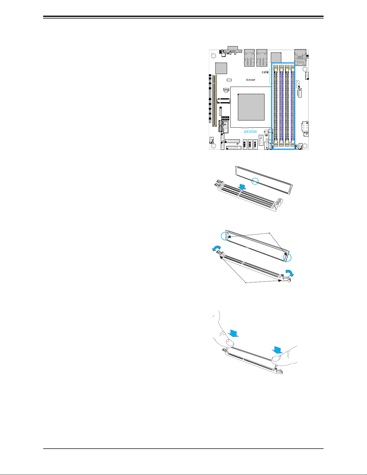
DIMM Module Population Sequence
When installing memory modules, the DIMM slots should be populated in the following order:
DIMMA2, then DIMMB2, DIMMA1, and then DIMMB1.
• Always use DDR4 DIMM modules of the same type and speed.
• Mixed DIMM speeds can be installed. However, all DIMMs will run at the speed of the
slowest DIMM.
• The motherboard will support odd-numbered modules (one or three modules installed).
However, for best memory performance, install DIMM modules in pairs to activate memory
interleaving.
JBM1
JI2C1
JI2C2
JD1
JPG1
JWD1
JVRM1
JVRM2
JVR1
LED1
UID
LED2
M2_SRW1
BMC
AST2500
1-3:PWR LEDJD1:
4-7:SPEAKER
JPCIE1
CPU SLOT7 PCI-E 3.0 X16
JPG1:
VGA
JWD1:WATCH DOG
JMD2
PCI-E 3.0 X4 M.2-HC
J1
SGPIO1
2-3:DISABLE
1-2:RST
2-3:NMI
JHDT1
LEDM1
1-2:ENABLE
JI2C1/JI2C2:
1-2:ENABLE
2-3:DISABLE
VGA
LAN 3/4
M11SDV-4CT-LN4F
DESIGNED IN USA
REV:1.01A
CPU
LAN 1/2
i350
BAR CODE
1
DIMMA1
JSMB
DIMMA2
IPMI_LAN
USB 6/7(3.0)
DIMMB2
DIMMB1
JPI2C1
USB 4/5
JPV1
JBM2
DIMMA1
DIMMA2
DIMMB1
DIMMB2
BT1
NIC
NIC HDD
PWR
OH/FF
PWR
RST
X
X
NMI
1
UID
2
LED
JGP1
COM1
FANA
USB 0/1
USB 2/3
JTPM1
JF1
ON
JF1
LED3
LED
SATA2
SATA3
SUPER DOM
SATA POWER
JBT1
J6
FAN2
JSTBY1
SATA0
SATA1
PJ1
FAN1
27
Page 28
Super M11SDV-4C/4CT/8C/8CT/8C+-LN4F User's Manual
FAN2
JSTBY1
SATA POWER
DIMM Installation
1. Insert the desired number of DIMMs into
the memory slots, starting with DIMMA2,
DIMMB2, DIMMA1, DIMMB1. For best
performance, please use the memory
modules of the same type and speed.
2. Push the release tabs outwards on both
ends of the DIMM slot to unlock it.
3. Align the key of the DIMM module with the
receptive point on the memory slot.
4. Align the notches on both ends of the
module against the receptive points on the
ends of the slot.
5. Press both ends of the module straight
down into the slot until the module snaps
into place.
VGA
LED1
UID
LED2
LEDM1
M2_SRW1
BMC
AST2500
JBM1
JI2C1/JI2C2:
1-3:PWR LEDJD1:
JI2C1
1-2:ENABLE
4-7:SPEAKER
2-3:DISABLE
JI2C2
JPCIE1
CPU SLOT7 PCI-E 3.0 X16
JPG1:
1-2:ENABLE
VGA
2-3:DISABLE
JWD1:WATCH DOG
1-2:RST
2-3:NMI
JD1
JMD2
PCI-E 3.0 X4 M.2-HC
JPG1
JWD1
J1
JVRM1
JVRM2
JHDT1
JVR1
SGPIO1
JGP1
COM1
FANA
USB 0/1
USB 2/3
LAN 3/4
M11SDV-4CT-LN4F
DESIGNED IN USA
REV:1.01A
CPU
NIC
NICHDD
PWR
OH/FF
PWR
RST
X
X
NMI
1
UID
2
LED
LED
ON
JF1
JTPM1
JF1
SATA1
SATA2
LED3
i350
LAN 1/2
SATA0
SATA3
SUPER DOM
1
BAR CODE
BT1
JBT1
J6
JBM2
IPMI_LAN
USB 6/7(3.0)
USB 4/5
JSMB
JPI2C1
DIMMB2
DIMMA2
DIMMB1
DIMMA1
JPV1
PJ1
FAN1
6. Press the release tabs to the lock positions
to secure the DIMM module into the slot.
DIMM Removal
Press both release tabs on the ends of the
DIMM module to unlock it. Once the DIMM
module is loosened, remove it from the
memory slot.
Notches
Release Tabs
Press both notches
straight down into
the memory slot.
28
Page 29
Chapter 2: Installation
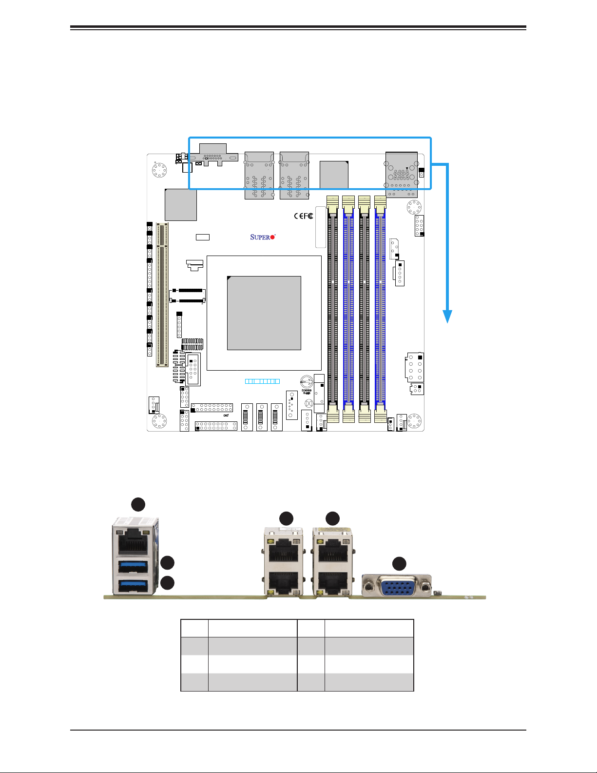
2.4 Rear I/O Ports
See Figure 2-1 below for the locations and descriptions of the various I/O ports on the rear
of the motherboard.
JI2C1
JI2C2
JD1
JWD1
JVRM1
JVRM2
JVR1
FANA
JBM1
JPG1
LED1
UID
LED2
M2_SRW1
BMC
AST2500
1-3:PWR LEDJD1:
4-7:SPEAKER
JPCIE1
CPU SLOT7 PCI-E 3.0 X16
JMD2
PCI-E 3.0 X4 M.2-HC
J1
SGPIO1
JGP1
USB 0/1
USB 2/3
JPG1:
VGA
2-3:DISABLE
JWD1:WATCH DOG
1-2:RST
2-3:NMI
JHDT1
1-2:ENABLE
LEDM1
JI2C1/JI2C2:
1-2:ENABLE
2-3:DISABLE
COM1
VGA
i350
LAN 3/4
M11SDV-4CT-LN4F
DESIGNED IN USA
REV:1.01A
CPU
NIC
OH/FF
PWR
RST
X
UID
2
ON
JF1
JTPM1
LED3
JF1
SATA2
LAN 1/2
NIC HDD
PWR
X
NMI
1
LED
LED
SATA0
SATA1
SUPER DOM
JBT1
SATA3
J6
SATA POWER
BAR CODE
BT1
FAN2
1
DIMMA1
JSTBY1
IPMI_LAN
USB 6/7(3.0)
JSMB
DIMMA2
DIMMB1
JBM2
USB 4/5
JPI2C1
DIMMB2
JPV1
PJ1
FAN1
Figure 2-1. I/O Port Locations and Denitions
1
54
2
3
# Decription # Description
1 IPMI_LAN 4 LAN1/2
2 USB7 5 LAN3/4
3 USB6 6 VGA
6
29
Page 30
Super M11SDV-4C/4CT/8C/8CT/8C+-LN4F User's Manual
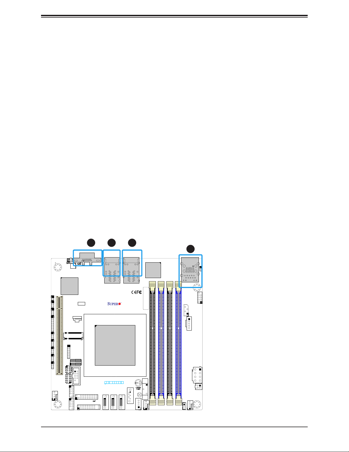
Video Graphics Array (VGA) Port
A (VGA) video port is located on the I/O back panel. Use this connection for a VGA display.
Local Area Network (LAN) Ports
There are four LAN ports located on the I/O back panel of the motherboard. LAN1 - LAN4
are 1 GbE RJ45 Ethernet ports. The motherboard also offers one IPMI LAN port.
1
32
4
UID
M2_SRW1
BMC
1-3:PWR LEDJD1:
4-7:SPEAKER
JPG1:
VGA
JWD1:WATCH DOG
JMD2
PCI-E 3.0 X4 M.2-HC
JHDT1
1-2:ENABLE
2-3:DISABLE
1-2:RST
2-3:NMI
LEDM1
JI2C1/JI2C2:
1-2:ENABLE
2-3:DISABLE
COM1
VGA
i350
LAN 3/4
M11SDV-4CT-LN4F
DESIGNED IN USA
REV:1.01A
OH/FF
PWR
RST
X
UID
ON
JF1
JTPM1
JF1
SATA2
LED3
LAN 1/2
CPU
NIC
NIC HDD
PWR
X
NMI
1
2
LED
LED
SATA0
SATA1
JBT1
SATA3
SUPER DOM
J6
SATA POWER
BAR CODE
BT1
FAN2
1
DIMMA1
JSTBY1
IPMI_LAN
USB 6/7(3.0)
JSMB
DIMMA2
JBM2
1. VGA Port
2. LAN3/4
USB 4/5
3. LAN1/2
4. IPMI LAN
JPI2C1
DIMMB2
DIMMB1
JPV1
PJ1
FAN1
LED1
LED2
AST2500
JBM1
JI2C1
JI2C2
JPCIE1
CPU SLOT7 PCI-E 3.0 X16
JD1
JPG1
JWD1
J1
JVRM1
JVRM2
JVR1
SGPIO1
JGP1
FANA
USB 0/1
USB 2/3
30
Page 31

Chapter 2: Installation
Universal Serial Bus (USB) Ports
There are two (2) USB 3.0 ports (USB6/7) on the I/O back panel. The motherboard also has
six (6) USB 2.0 headers that provide six (6) USB 2.0 ports (USB0/1, USB2/3, USB4/5). The
onboard header can be used to provide front side USB access with a cable (not included).
Front Panel USB 0/1, USB 2/3, USB 4/5 (2.0)
Pin Denitions
Pin# Denition Pin# Denition
1 +5V 2 +5V
3 USB_N 4 USB_N
5 USB_P 6 USB_P
7 Ground 8 Ground
9 Key 10 Ground
LED1
LED2
VGA
UID
LEDM1
M2_SRW1
i350
4
JBM2
1. USB0/1
BMC
AST2500
JBM1
JI2C1/JI2C2:
1-3:PWR LEDJD1:
JI2C1
JI2C2
JD1
JPG1
JWD1
JVRM1
JVRM2
JVR1
1
FANA
2
4-7:SPEAKER
JPCIE1
CPU SLOT7 PCI-E 3.0 X16
JMD2
PCI-E 3.0 X4 M.2-HC
J1
SGPIO1
JGP1
USB 0/1
USB 2/3
JPG1:
1-2:ENABLE
VGA
2-3:DISABLE
JWD1:WATCH DOG
1-2:RST
2-3:NMI
JHDT1
COM1
1-2:ENABLE
2-3:DISABLE
JTPM1
LED3
JF1
LAN 3/4
M11SDV-4CT-LN4F
DESIGNED IN USA
REV:1.01A
OH/FF
PWR
RST
X
UID
ON
JF1
SATA2
LAN 1/2
CPU
NIC
NIC HDD
PWR
X
NMI
1
2
LED
LED
SATA0
SATA1
JBT1
SATA3
SUPER DOM
J6
SATA POWER
BAR CODE
BT1
FAN2
1
IPMI_LAN
USB 6/7(3.0)
USB 4/5
JSMB
JPI2C1
DIMMB2
DIMMA2
DIMMB1
DIMMA1
FAN1
JSTBY1
3
JPV1
PJ1
2. USB2/3
3. USB4/5
4. USB6/7
31
Page 32

Super M11SDV-4C/4CT/8C/8CT/8C+-LN4F User's Manual
Unit Identier Switch/UID LED Indicator
A Unit Identier (UID) switch and an LED indicator are located on the motherboard. The UID
switch is located next to the VGA port on the back panel. The UID LED is located at LED1,
next to the UID switch. When you press the UID switch, the UID LED will be turned on.
Press the UID switch again to turn off the LED indicator. The LED indicator provides easy
identication of a system unit that may be in need of service.
Note: UID can also be triggered via IPMI on the motherboard. For more information
on IPMI, please refer to the IPMI User's Guide posted on our website at https://www.
supermicro.com/support/manuals/.
UID Switch
Pin Denitions
Pin# Denition
1 Ground
Color Status
Blue: On Unit Identied
UID LED
Pin Denitions
2 Ground
3 Button In
4 Button In
1
2
UID
M2_SRW1
1-3:PWR LEDJD1:
4-7:SPEAKER
JPG1:
VGA
2-3:DISABLE
JWD1:WATCH DOG
1-2:RST
2-3:NMI
JMD2
PCI-E 3.0 X4 M.2-HC
JHDT1
1-2:ENABLE
LEDM1
JI2C1/JI2C2:
1-2:ENABLE
2-3:DISABLE
VGA
LAN 3/4
M11SDV-4CT-LN4F
DESIGNED IN USA
REV:1.01A
CPU
i350
LAN 1/2
BAR CODE
1
DIMMA1
IPMI_LAN
USB 6/7(3.0)
JSMB
DIMMA2
JBM2
1. UID Switch
2. UID LED (LED1)
USB 4/5
JPI2C1
DIMMB2
DIMMB1
JPV1
JBM1
JI2C1
JI2C2
JD1
JPG1
JWD1
JVRM1
JVRM2
JVR1
LED1
LED2
BMC
AST2500
JPCIE1
CPU SLOT7 PCI-E 3.0 X16
J1
SGPIO1
NIC
NIC HDD
PWR
OH/FF
PWR
RST
X
X
NMI
1
UID
2
LED
LED
JGP1
FANA
COM1
USB 0/1
USB 2/3
JTPM1
JF1
ON
JF1
SATA0
SATA1
SATA2
LED3
BT1
JBT1
SATA3
SUPER DOM
J6
SATA POWER
FAN2
JSTBY1
PJ1
FAN1
32
Page 33

Chapter 2: Installation
2.5 Front Control Panel
JF1 contains header pins for various buttons and indicators that are normally located on a
control panel at the front of the chassis. These connectors are designed specically for use
with Supermicro chassis. See the gure below for the descriptions of the front control panel
buttons and LED indicators.
FANA
JBM1
JI2C1
JI2C2
JD1
JPG1
JWD1
JVRM1
JVRM2
JVR1
LED1
UID
LED2
M2_SRW1
BMC
AST2500
1-3:PWR LEDJD1:
4-7:SPEAKER
JPCIE1
CPU SLOT7 PCI-E 3.0 X16
JMD2
PCI-E 3.0 X4 M.2-HC
J1
SGPIO1
JGP1
USB 0/1
USB 2/3
JPG1:
1-2:ENABLE
VGA
2-3:DISABLE
JWD1:WATCH DOG
1-2:RST
2-3:NMI
JHDT1
LEDM1
JI2C1/JI2C2:
1-2:ENABLE
2-3:DISABLE
COM1
VGA
i350
LAN 3/4
M11SDV-4CT-LN4F
DESIGNED IN USA
REV:1.01A
CPU
NIC
OH/FF
PWR
RST
X
UID
2
ON
JF1
JTPM1
LED3
JF1
SATA2
LAN 1/2
NIC HDD
PWR
X
NMI
1
LED
LED
SATA0
SATA1
SATA3
SUPER DOM
SATA POWER
JBT1
J6
BAR CODE
BT1
FAN2
1
IPMI_LAN
USB 6/7(3.0)
JSMB
DIMMA2
DIMMA1
JSTBY1
DIMMB1
JBM2
USB 4/5
JPI2C1
DIMMB2
JPV1
PJ1
FAN1
Figure 2-2. JF1 Header Pins
12
PWR
Reset
Power Button
Reset Button
Ground
Ground
3.3V* Power Fail LED*
19
OH/Fan Fail LED
NIC2 Activity LED
NIC1 Activity LED
HDD LED
FP PWRLED
X
Ground
20
UID LED*
3.3V Stby
3.3V Stby
3.3V Stby
3.3V Stby
X
NMI
33
Page 34

Super M11SDV-4C/4CT/8C/8CT/8C+-LN4F User's Manual
Power Button
The Power Button connection is located on pins 1 and 2 of JF1. Momentarily contacting both
pins will power on/off the system. This button can also be congured to function as a suspend
button (with a setting in the BIOS - see Chapter 4). To turn off the power when the system
is in suspend mode, press the button for 4 seconds or longer. Refer to the table below for
pin denitions.
Power Button
Pin Denitions (JF1)
Pin# Denition
1 Power On
2 Ground
Reset Button
The Reset Button connection is located on pins 3 and 4 of JF1. Attach it to a hardware reset
switch on the computer case. Refer to the table below for pin denitions.
Reset Button
Pin Denitions (JF1)
Pin# Denition
3 Reset
4 Ground
12
PWR
Reset
Power Button
Reset Button
3.3V* Power Fail LED*
UID LED*
3.3V Stby
3.3V Stby
3.3V Stby
3.3V Stby
X
NMI
19
1
2
Ground
Ground
OH/Fan Fail LED
NIC2 Activity LED
NIC1 Activity LED
HDD LED
FP PWRLED
X
Ground
20
1. PWR Button
2. Reset Button
34
Page 35

Chapter 2: Installation
Overheat (OH)/Fan Fail/PWR Fail LED
Connect an LED cable to pins 7 and 8 to use the Overheat (OH)/Fan Fail/PWR Fail LED
connections. The LED on pin 8 provides warnings of overheat, fan failure, or power failure.
Refer to the tables below for pin denitions.
OH/Fan Fail Indicator Status
State Denition
Off Normal
On Overheat
Flashing Fan Fail/PWR Fail
OH/Fan Fail LED
Pin Denitions (JF1)
Pin# Denition
7 Blue UID LED
8 OH/Fan Fail/PWR Fail LED
LAN1/LAN2 Activity LED
The LAN LED connection for LAN port 1 is located on pins 11 and 12 of JF1, and the LED
connection for LAN port 2 is on pins 9 and 10. Attach the NIC LED cables here to display
network activity. Refer to the table below for pin denitions.
LAN1/LAN2 LED
Pin Denitions (JF1)
Pin# Denition
9 +3.3 Stby
10 LAN2 Activity LED
11 +3.3 Stby
12 LAN1 Activity LED
PWR
Reset
12
Power Button
Reset Button
3.3V* Power Fail LED*
UID LED*
3.3V Stby
3.3V Stby
3.3V Stby
3.3V Stby
X
NMI
20
19
Ground
Ground
OH/Fan Fail LED
NIC2 Activity LED
NIC1 Activity LED
HDD LED
FP PWRLED
X
Ground
35
1. OH/Fan Fail/PWR Fail LED
2. NIC2 Activity LED
3. NIC1 Activity LED
1
2
3
Page 36

Super M11SDV-4C/4CT/8C/8CT/8C+-LN4F User's Manual
HDD LED
The HDD LED connection is located on pins 13 and 14 of JF1. Attach a cable to show the
hard drive activity status. Refer to the table below for pin denitions.
HDD LED
Pin Denitions (JF1)
Pin# Denition
13 3.3V Stdby
14 HDD LED
Power LED
The Power LED connection is located on pins 15 and 16 of JF1. Refer to the table below
for pin denitions.
PWR
Reset
Power LED
Pin Denitions (JF1)
Pin# Denition
15 3.3V
16 PWR LED
12
Power Button
Reset Button
3.3V* Power Fail LED*
UID LED*
3.3V Stby
3.3V Stby
3.3V Stby
3.3V Stby
X
NMI
20
19
Ground
Ground
OH/Fan Fail LED
NIC2 Activity LED
NIC1 Activity LED
HDD LED
FP PWRLED
X
Ground
1
1. HDD LED
2. PWR LED
2
36
Page 37

Chapter 2: Installation
Power Fail LED
Connect an LED cable to Power Fail connections on pins 5 and 6 of JF1 to provide warnings
for a power failure. Refer to the table below for pin denitions.
OH/Fan Fail Indicator
Status
Pin # Denition
5 3.3V
6 PWR Fail LED
PWR
Reset
12
Power Button
Reset Button
3.3V* Power Fail LED*
UID LED*
3.3V Stby
3.3V Stby
3.3V Stby
3.3V Stby
X
NMI
20
19
37
Ground
Ground
OH/Fan Fail LED
NIC2 Activity LED
NIC1 Activity LED
HDD LED
FP PWRLED
X
Ground
1. Power Fail LED
1
Page 38

Super M11SDV-4C/4CT/8C/8CT/8C+-LN4F User's Manual
2.6 Connectors and Headers
Power Connections
Main ATX Power Supply Connector
JPV1 is the 12V DC power connector, a required input for either ATX or 12V DC power source.
In addition, when using ATX power, PJ1 is a necessary connection to the 24-pin ATX power
header from the PSU via PN: CBL-PWEX-1063. Refer to instructions in section 1.6.
8-pin 12V Power (JPV1)
Pin Denitions
Pins Denition
1 - 4 Ground
5 - 8 +12V
4-pin to ATX Power Signal (PJ1)
Pin Denitions
Pin# Denition
1 PWR_OK
2 GND
3 5VSB
4 PS_ON
HDD Power Connector
J6 is a 4-pin power connector for HDD use. It provides power from the motherboard to the
onboard HDD.
4-pin HDD Power
Pin Denitions
Pin# Denition
1 12V
2-3 GND
4 5V
UID
M2_SRW1
BMC
AST2500
1-3:PWR LEDJD1:
4-7:SPEAKER
JMD2
PCI-E 3.0 X4 M.2-HC
J1
JPG1:
VGA
2-3:DISABLE
JWD1:WATCH DOG
1-2:RST
2-3:NMI
JHDT1
1-2:ENABLE
VGA
LEDM1
LAN 1/2
CPU
NIC
NIC HDD
PWR
X
NMI
1
2
LED
LED
SATA0
SATA1
SATA3
SUPER DOM
3
SATA POWER
JI2C1/JI2C2:
1-2:ENABLE
2-3:DISABLE
COM1
LAN 3/4
M11SDV-4CT-LN4F
DESIGNED IN USA
REV:1.01A
OH/FF
PWR
RST
X
UID
ON
JF1
JTPM1
JF1
SATA2
LED3
JBT1
J6
i350
BAR CODE
BT1
FAN2
JBM2
IPMI_LAN
1
USB 6/7(3.0)
USB 4/5
JSMB
JPI2C1
DIMMB2
DIMMA2
DIMMB1
DIMMA1
JPV1
PJ1
FAN1
JSTBY1
1. 8-Pin 12V ATX Power
2. 4-pin to ATX Power Connector
3. 4-pin HDD Power Connector
1
2
LED1
LED2
JBM1
JI2C1
JI2C2
JPCIE1
CPU SLOT7 PCI-E 3.0 X16
JD1
JPG1
JWD1
JVRM1
JVRM2
JVR1
SGPIO1
JGP1
FANA
USB 0/1
USB 2/3
38
Page 39

Chapter 2: Installation
Headers
General Purpose I/O Header
The JGP1 (General Purpose Input/Output) header is a general purpose I/O expander on a
pin header via the SMBus. Refer to the table below for pin denitions.
JGP1 Header
Pin Denitions
Pin# Denition
1 3.3V Stdby
2 Ground
3 GP0
4 GP1
5 GP2
6 GP3
7 GP4
8 GP5
9 GP6
10 GP7
1. General Purpose I/O Header
UID
M2_SRW1
BMC
1-3:PWR LEDJD1:
4-7:SPEAKER
JPG1:
VGA
JMD2
PCI-E 3.0 X4 M.2-HC
J1
1-2:ENABLE
2-3:DISABLE
JWD1:WATCH DOG
1-2:RST
2-3:NMI
JHDT1
LEDM1
COM1
JI2C1/JI2C2:
1-2:ENABLE
2-3:DISABLE
VGA
i350
LAN 3/4
M11SDV-4CT-LN4F
DESIGNED IN USA
REV:1.01A
OH/FF
PWR
RST
X
UID
ON
JF1
JTPM1
JF1
SATA2
LED3
LAN 1/2
CPU
NIC
NIC HDD
PWR
X
NMI
1
2
LED
LED
SATA0
SATA1
JBT1
SATA3
SUPER DOM
J6
SATA POWER
BAR CODE
BT1
FAN2
1
JSTBY1
JBM2
IPMI_LAN
USB 6/7(3.0)
USB 4/5
JSMB
JPI2C1
DIMMB2
DIMMA2
DIMMB1
DIMMA1
JPV1
PJ1
FAN1
LED1
LED2
AST2500
JBM1
JI2C1
JI2C2
JPCIE1
CPU SLOT7 PCI-E 3.0 X16
JD1
JPG1
JWD1
JVRM1
JVRM2
JVR1
SGPIO1
1
JGP1
FANA
USB 0/1
USB 2/3
39
Page 40

Super M11SDV-4C/4CT/8C/8CT/8C+-LN4F User's Manual
Standby Power
The Standby Power header is located at JSTBY1 on the motherboard. Refer to the table
below for pin denitions.
Standby Power
Pin Denitions
Pin# Denition
1 +5V Standby
2 Ground
3 No Connection
1. Standby Power
UID
M2_SRW1
BMC
1-3:PWR LEDJD1:
4-7:SPEAKER
JPG1:
JMD2
PCI-E 3.0 X4 M.2-HC
1-2:ENABLE
VGA
2-3:DISABLE
JWD1:WATCH DOG
1-2:RST
2-3:NMI
JHDT1
LEDM1
COM1
JI2C1/JI2C2:
1-2:ENABLE
2-3:DISABLE
VGA
i350
LAN 3/4
M11SDV-4CT-LN4F
DESIGNED IN USA
REV:1.01A
OH/FF
PWR
RST
X
UID
ON
JF1
JTPM1
JF1
SATA2
LED3
LAN 1/2
CPU
NIC
NIC HDD
PWR
X
NMI
1
2
LED
LED
SATA0
SATA1
JBT1
SATA3
SUPER DOM
J6
SATA POWER
BAR CODE
BT1
FAN2
1
JSTBY1
JBM2
IPMI_LAN
USB 6/7(3.0)
USB 4/5
JSMB
JPI2C1
DIMMB2
DIMMA2
DIMMB1
DIMMA1
JPV1
PJ1
1
FAN1
LED1
LED2
AST2500
JBM1
JI2C1
JI2C2
JPCIE1
CPU SLOT7 PCI-E 3.0 X16
JD1
JPG1
JWD1
J1
JVRM1
JVRM2
JVR1
SGPIO1
JGP1
FANA
USB 0/1
USB 2/3
40
Page 41

Chapter 2: Installation
FAN2
Fan Headers
The M11SDV-4C/4CT/8C/8CT/8C+-LN4F has three 4-pin fan headers (FAN1, FAN2, FANA).
These headers are backwards-compatible with the traditional 3-pin fans. This motherboard
supports dual cooling zone. (Zone1:FAN1/2, Zone2:FANA). Fan speed control is available for
4-pin fans only by Thermal Management via the IPMI 2.0 interface. Refer to the table below
for pin denitions.
Fan Header
Pin Denitions
Pin# Denition
1 Ground (Black)
2 2.5A/+12V (Red)
3 Tachometer
4 PWM_Control
Speaker Header
On the JD1 header, pins 4-7 are for the external speaker.
Speaker Connector
Pin Denitions
Pin# Denition
1 3.3V
2 PWR_LED_IN
3 PWR_LED_IN
4 +5V
5 NC
6 NC
7 SPK_IN
UID
M2_SRW1
BMC
AST2500
1-3:PWR LEDJD1:
4-7:SPEAKER
JMD2
PCI-E 3.0 X4 M.2-HC
J1
JPG1:
1-2:ENABLE
VGA
2-3:DISABLE
JWD1:WATCH DOG
1-2:RST
2-3:NMI
JHDT1
VGA
LEDM1
LAN 1/2
CPU
JI2C1/JI2C2:
1-2:ENABLE
2-3:DISABLE
LAN 3/4
M11SDV-4CT-LN4F
DESIGNED IN USA
REV:1.01A
i350
BAR CODE
JBM2
IPMI_LAN
1
USB 6/7(3.0)
USB 4/5
JSMB
JPI2C1
DIMMB2
DIMMA2
DIMMB1
DIMMA1
JPV1
1. FAN1
2. FAN2
3. FANA
4. Speaker Header
LED1
LED2
JBM1
JI2C1
JI2C2
JPCIE1
CPU SLOT7 PCI-E 3.0 X16
JD1
4
JPG1
JWD1
JVRM1
JVRM2
JVR1
SGPIO1
NIC
NIC HDD
PWR
OH/FF
PWR
RST
X
X
NMI
1
UID
2
LED
LED
JGP1
3
FANA
COM1
USB 0/1
USB 2/3
JTPM1
ON
JF1
SATA0
SATA1
SATA2
LED3
JF1
BT1
PJ1
JBT1
SATA3
SUPER DOM
J6
SATA POWER
2
1
FAN1
JSTBY1
41
Page 42

Super M11SDV-4C/4CT/8C/8CT/8C+-LN4F User's Manual
SATA Ports
Four SATA 3.0 connectors (SATA0-4), supported by the AMD EPYC™ 3000 chipset, are
located on the M11SDV-4C/4CT/8C/8CT/8C+-LN4F motherboard. These SATA ports support
RAID 0, 1, 5, and 10. Refer to the tables below for pin denitions.
SATA 3.0 Port
Pin Denitions
Pin# Signal
1 Ground
2 SATA_TXP
3 SATA_TXN
4 Ground
5 SATA_RXN
6 SATA_RXP
7 Ground
BMC
AST2500
JMD2
PCI-E 3.0 X4 M.2-HC
J1
JGP1
UID
M2_SRW1
1-3:PWR LEDJD1:
4-7:SPEAKER
JPG1:
VGA
JWD1:WATCH DOG
JHDT1
2-3:DISABLE
1-2:RST
2-3:NMI
1-2:ENABLE
VGA
LEDM1
LAN 1/2
LAN 3/4
JI2C1/JI2C2:
1-2:ENABLE
2-3:DISABLE
COM1
JTPM1
M11SDV-4CT-LN4F
DESIGNED IN USA
REV:1.01A
CPU
NIC
NIC HDD
PWR
OH/FF
PWR
RST
X
ON
JF1
LED3
JF1
3
4
X
NMI
1
UID
2
LED
LED
SATA0
SATA1
SATA2
SATA3
SUPER DOM
SATA POWER
12
J6
JBT1
i350
BAR CODE
BT1
FAN2
JBM2
IPMI_LAN
1
USB 6/7(3.0)
USB 4/5
JSMB
JPI2C1
DIMMB2
DIMMA2
DIMMB1
DIMMA1
JPV1
PJ1
FAN1
JSTBY1
LED1
LED2
JBM1
JI2C1
JI2C2
JPCIE1
CPU SLOT7 PCI-E 3.0 X16
JD1
JPG1
JWD1
JVRM1
JVRM2
JVR1
SGPIO1
FANA
USB 0/1
USB 2/3
1. SATA0
2. SATA1
3. SATA2
4. SATA3
42
Page 43

Chapter 2: Installation
System Management Bus Header
A System Management Bus header for additional slave devices or sensors is located at JSMB.
See the table below for pin denitions.
SMBus Header
Pin Denitions
Pin# Denition
1 Data
2 Ground
3 Clock
4 NC
Power SMB (I2C) Header
The Power System Management Bus (I2C) connector (JPI2C1) monitors the power supply,
fan, and system temperatures. Refer to the table below for pin denitions.
Power SMB Header
Pin Denitions
Pin# Denition
1 Clock
2 Data
3 PWRFAIL_N
4 Ground
5 NC
UID
M2_SRW1
BMC
1-3:PWR LEDJD1:
4-7:SPEAKER
JMD2
PCI-E 3.0 X4 M.2-HC
J1
JPG1:
VGA
JWD1:WATCH DOG
1-2:RST
2-3:NMI
JHDT1
1-2:ENABLE
2-3:DISABLE
LEDM1
JI2C1/JI2C2:
1-2:ENABLE
2-3:DISABLE
COM1
VGA
i350
LAN 3/4
M11SDV-4CT-LN4F
DESIGNED IN USA
REV:1.01A
OH/FF
PWR
RST
X
UID
ON
JF1
JTPM1
JF1
SATA2
LED3
LAN 1/2
CPU
NIC
NIC HDD
PWR
X
NMI
1
2
LED
LED
SATA0
SATA1
JBT1
SATA3
SUPER DOM
J6
SATA POWER
BAR CODE
BT1
FAN2
1
JSTBY1
JBM2
IPMI_LAN
USB 6/7(3.0)
1
USB 4/5
JSMB
JPI2C1
2
DIMMB2
DIMMA2
DIMMB1
DIMMA1
JPV1
PJ1
FAN1
LED1
LED2
AST2500
JBM1
JI2C1
JI2C2
JPCIE1
CPU SLOT7 PCI-E 3.0 X16
JD1
JPG1
JWD1
JVRM1
JVRM2
JVR1
SGPIO1
JGP1
FANA
USB 0/1
USB 2/3
1. SMBus Header
2. Power SMB I2C
43
Page 44

Super M11SDV-4C/4CT/8C/8CT/8C+-LN4F User's Manual
M.2 Slot
M.2 is formerly known as Next Generation Form Factor (NGFF) and is designed for internal
mounting devices. The M11SDV-4C/4CT/8C/8CT/8C+-LN4F board has one M.2 connector at
JMD2. Interfaces are PCIEx4 and SATA 3.0.
COM Header
The motherboard has one COM port header (COM1) to provide a serial connection.
COM Port
Pin Denitions
Pin# Denition Pin# Denition
1 SP_DCDA 6 SP_DSRA
2 SP_RXDA 7 SP_RTSA
3 SP_TXDA 8 SP_CTSA
4 SP_DTRA 9 SP_RIA
5 GND 10 NC
UID
M2_SRW1
BMC
AST2500
1-3:PWR LEDJD1:
4-7:SPEAKER
JMD2
PCI-E 3.0 X4 M.2-HC
J1
JPG1:
VGA
JWD1:WATCH DOG
1
VGA
LEDM1
LAN 3/4
JI2C1/JI2C2:
1-2:ENABLE
2-3:DISABLE
1-2:ENABLE
2-3:DISABLE
1-2:RST
2-3:NMI
JHDT1
2
COM1
JTPM1
JF1
M11SDV-4CT-LN4F
DESIGNED IN USA
REV:1.01A
OH/FF
PWR
RST
X
UID
ON
JF1
SATA2
LED3
LAN 1/2
CPU
NIC
NIC HDD
PWR
X
NMI
1
2
LED
LED
SATA0
SATA1
SATA3
SUPER DOM
SATA POWER
JBT1
J6
i350
BAR CODE
BT1
FAN2
JBM2
IPMI_LAN
1
USB 6/7(3.0)
USB 4/5
JSMB
JPI2C1
DIMMB2
DIMMA2
DIMMB1
DIMMA1
JPV1
PJ1
FAN1
JSTBY1
1. M.2 Connector JMD2
2. COM1
LED1
LED2
JBM1
JI2C1
JI2C2
JPCIE1
CPU SLOT7 PCI-E 3.0 X16
JD1
JPG1
JWD1
JVRM1
JVRM2
JVR1
SGPIO1
JGP1
FANA
USB 0/1
USB 2/3
44
Page 45

Chapter 2: Installation
TPM/Port 80 Header
The JTPM1 header is used to connect a Trusted Platform Module (TPM). A TPM is a security
device that supports encryption and authentication in hard drives. It enables the motherboard
to deny access if the TPM associated with the hard drive is not installed in the system. Refer
to the table below for pin denitions.
Trusted Platform Module Header
Pin Denitions
Pin# Denition Pin# Denition
1 LCLK 2 GND1
3 LFRAME# 4 No Pin
5 LRESET# 6 +5V/NC
7 LAD3 8 LAD2
9 +3.3V 10 LAD1
11 LAD0 12 GND2
13 SMB_CLK 14 SMB_DAT
15 +3.3V_DUAL 16 SERIRQ
17 GND3 18 CLKRUN#/NC
19 LPCPD# 20 LDRQ# (X)
LED1
LED2
VGA
UID
LEDM1
M2_SRW1
i350
JBM2
1. TPM Header
BMC
AST2500
JBM1
JI2C1/JI2C2:
1-3:PWR LEDJD1:
JI2C1
JI2C2
JD1
JPG1
JWD1
JVRM1
JVRM2
JVR1
FANA
4-7:SPEAKER
JPCIE1
CPU SLOT7 PCI-E 3.0 X16
JMD2
PCI-E 3.0 X4 M.2-HC
J1
SGPIO1
JGP1
USB 0/1
USB 2/3
JPG1:
VGA
JWD1:WATCH DOG
JHDT1
2-3:DISABLE
1-2:RST
2-3:NMI
1-2:ENABLE
COM1
1-2:ENABLE
2-3:DISABLE
1
JTPM1
JF1
LAN 3/4
M11SDV-4CT-LN4F
DESIGNED IN USA
REV:1.01A
OH/FF
PWR
RST
X
UID
ON
JF1
SATA2
LED3
LAN 1/2
CPU
NIC
NIC HDD
PWR
X
NMI
1
2
LED
LED
SATA0
SATA1
JBT1
SATA3
SUPER DOM
J6
SATA POWER
BAR CODE
BT1
FAN2
1
IPMI_LAN
USB 6/7(3.0)
USB 4/5
JSMB
JPI2C1
DIMMB2
DIMMA2
DIMMB1
DIMMA1
JPV1
PJ1
FAN1
JSTBY1
45
Page 46

Super M11SDV-4C/4CT/8C/8CT/8C+-LN4F User's Manual
2.7 Jumper Settings
How Jumpers Work
To modify the operation of the motherboard, jumpers can be used to choose between optional
settings. Jumpers create shorts between two pins to change the function of the connector.
Pin 1 is identied with a square solder pad on the printed circuit board. See the diagram
below for an example of jumping pins 1 and 2. Refer to the motherboard layout page for
jumper locations.
Note: On two-pin jumpers, Closed means the jumper is on the pins and Open means
the jumper is off.
Connector
Pins
Jumper
Setting
3 2 1
3 2 1
46
Page 47

Chapter 2: Installation
CMOS Clear
JBT1 is used to clear the CMOS. Instead of pins, this jumper consists of contact pads to
prevent accidental clearing of the CMOS. To clear the CMOS, use a metal object such as a
small screwdriver to touch both pads at the same time to short the connection.
To Clear CMOS:
1. First power down the system and unplug the power cord(s).
2. Remove the cover of the chassis to access the motherboard.
3. Remove the onboard battery and the external CMOS battery installed on J18.
4. Short the CMOS pads with a metal object such as a small screwdriver for at least four
seconds.
5. Remove the screwdriver (or shorting device).
6. Install the batteries, the cover, reconnect the power cord(s), and power on the system.
Note: Clearing CMOS will also clear all passwords.
JBT1 contact pads
UID
M2_SRW1
BMC
AST2500
1-3:PWR LEDJD1:
4-7:SPEAKER
JMD2
PCI-E 3.0 X4 M.2-HC
J1
JPG1:
VGA
JWD1:WATCH DOG
1-2:RST
2-3:NMI
JHDT1
1-2:ENABLE
2-3:DISABLE
LEDM1
JI2C1/JI2C2:
1-2:ENABLE
2-3:DISABLE
VGA
1. CMOS Clear
LAN 3/4
M11SDV-4CT-LN4F
DESIGNED IN USA
REV:1.01A
CPU
i350
LAN 1/2
BAR CODE
1
JBM2
IPMI_LAN
USB 6/7(3.0)
USB 4/5
JSMB
JPI2C1
DIMMB2
DIMMA2
DIMMB1
DIMMA1
JPV1
JBM1
JI2C1
JI2C2
JD1
JPG1
JWD1
JVRM1
JVRM2
JVR1
LED1
LED2
JPCIE1
CPU SLOT7 PCI-E 3.0 X16
SGPIO1
NIC
NIC HDD
PWR
OH/FF
PWR
RST
X
X
NMI
1
UID
2
LED
LED
JGP1
FANA
COM1
USB 0/1
USB 2/3
JTPM1
ON
JF1
SATA0
SATA1
SATA2
LED3
JF1
BT1
JBT1
SATA3
SUPER DOM
1
J6
SATA POWER
FAN2
JSTBY1
PJ1
FAN1
47
Page 48

Super M11SDV-4C/4CT/8C/8CT/8C+-LN4F User's Manual
SMBus to PCI-E Slots
Jumpers JI2C1 and JI2C2 allow you to connect the System Management Bus (I2C) to the
PCI-E slots. Both jumpers must be set to the same setting (JI2C1 controls the clock and
JI2C2 controls the data). The default setting is Disabled. Refer to the table below for more
information.
SMBus to PCI-E Slots
Jumper Settings
Jumper Setting Denition
Pins 1-2 Enabled
Pins 2-3 Disabled (Default)
UID
M2_SRW1
BMC
1-3:PWR LEDJD1:
4-7:SPEAKER
JMD2
PCI-E 3.0 X4 M.2-HC
J1
JPG1:
VGA
2-3:DISABLE
JWD1:WATCH DOG
1-2:RST
2-3:NMI
JHDT1
1-2:ENABLE
LEDM1
JI2C1/JI2C2:
1-2:ENABLE
2-3:DISABLE
COM1
VGA
1. JI2C1
i350
LAN 3/4
M11SDV-4CT-LN4F
DESIGNED IN USA
REV:1.01A
OH/FF
PWR
RST
X
UID
ON
JF1
JTPM1
JF1
SATA2
LED3
LAN 1/2
CPU
NIC
NIC HDD
PWR
X
NMI
1
2
LED
LED
SATA0
SATA1
JBT1
SATA3
SUPER DOM
J6
SATA POWER
BAR CODE
BT1
FAN2
1
JSTBY1
JBM2
IPMI_LAN
USB 6/7(3.0)
USB 4/5
JSMB
JPI2C1
DIMMB2
DIMMA2
DIMMB1
DIMMA1
JPV1
PJ1
FAN1
2. JI2C2
LED1
LED2
AST2500
JBM1
JI2C1
1
JI2C2
JPCIE1
2
CPU SLOT7 PCI-E 3.0 X16
JD1
JPG1
JWD1
JVRM1
JVRM2
JVR1
SGPIO1
JGP1
FANA
USB 0/1
USB 2/3
48
Page 49

Chapter 2: Installation
VGA Enable/Disable
JPG1 allows the user to enable the VGA connector. The default setting is Enabled. Refer to
the table below for more information.
VGA Enable/Disable
Jumper Settings
Jumper Setting Denition
Pins 1-2 Enabled (Default)
Pins 2-3 Disabled
UID
M2_SRW1
BMC
AST2500
1-3:PWR LEDJD1:
4-7:SPEAKER
JMD2
PCI-E 3.0 X4 M.2-HC
J1
JPG1:
VGA
JWD1:WATCH DOG
1-2:RST
2-3:NMI
JHDT1
1-2:ENABLE
2-3:DISABLE
LEDM1
JI2C1/JI2C2:
1-2:ENABLE
2-3:DISABLE
COM1
VGA
1. VGA Enable
i350
LAN 3/4
M11SDV-4CT-LN4F
DESIGNED IN USA
REV:1.01A
OH/FF
PWR
RST
X
UID
ON
JF1
JTPM1
JF1
SATA2
LED3
LAN 1/2
CPU
NIC
NIC HDD
PWR
X
NMI
1
2
LED
LED
SATA0
SATA1
JBT1
SATA3
SUPER DOM
J6
SATA POWER
BAR CODE
BT1
FAN2
1
JSTBY1
JBM2
IPMI_LAN
USB 6/7(3.0)
USB 4/5
JSMB
JPI2C1
DIMMB2
DIMMA2
DIMMB1
DIMMA1
JPV1
PJ1
FAN1
LED1
LED2
JBM1
JI2C1
JI2C2
JPCIE1
CPU SLOT7 PCI-E 3.0 X16
JD1
JPG1
1
JWD1
JVRM1
JVRM2
JVR1
SGPIO1
JGP1
FANA
USB 0/1
USB 2/3
49
Page 50

Super M11SDV-4C/4CT/8C/8CT/8C+-LN4F User's Manual
Watch Dog
JWD1 controls the Watch Dog function. Watch Dog is a monitor that can reboot the system
when a software application hangs. Jumping pins 1-2 will cause Watch Dog to reset the
system if an application hangs. Jumping pins 2-3 will generate a non-maskable interrupt
signal for the application that hangs. Watch Dog must also be enabled in BIOS. The default
setting is Reset.
Note: When Watch Dog is enabled, users need to write their own application software
to disable it.
Watch Dog
Jumper Settings
Jumper Setting Denition
Pins 1-2 Reset (Default)
Pins 2-3 NMI
Open Disabled
UID
M2_SRW1
BMC
1-3:PWR LEDJD1:
4-7:SPEAKER
JMD2
PCI-E 3.0 X4 M.2-HC
J1
JPG1:
VGA
JWD1:WATCH DOG
JHDT1
2-3:DISABLE
1-2:RST
2-3:NMI
1-2:ENABLE
LEDM1
COM1
JI2C1/JI2C2:
1-2:ENABLE
2-3:DISABLE
VGA
i350
LAN 3/4
M11SDV-4CT-LN4F
DESIGNED IN USA
REV:1.01A
OH/FF
PWR
RST
X
UID
ON
JF1
JTPM1
JF1
SATA2
LED3
LAN 1/2
CPU
NIC
NIC HDD
PWR
X
NMI
1
2
LED
LED
SATA0
SATA1
JBT1
SATA3
SUPER DOM
J6
SATA POWER
BAR CODE
BT1
FAN2
1
JSTBY1
JBM2
IPMI_LAN
USB 6/7(3.0)
USB 4/5
JSMB
JPI2C1
DIMMB2
DIMMA2
DIMMB1
DIMMA1
JPV1
PJ1
FAN1
LED1
LED2
AST2500
JBM1
JI2C1
JI2C2
JPCIE1
CPU SLOT7 PCI-E 3.0 X16
JD1
JPG1
JWD1
1
JVRM1
JVRM2
JVR1
SGPIO1
JGP1
FANA
USB 0/1
USB 2/3
1. Watch Dog Timer
50
Page 51

Chapter 2: Installation
I2C Bus for VRM
Jumpers JVRM1 and JVRM2 allow the BMC or the PCH to access CPU and memory VRM
controllers. Refer to the table below for jumper settings.
VRM
Jumper Settings
Jumper Setting Denition
Pins 1-2 BMC (Normal)
Pins 2-3 PCH
Disable IPMI/Share LAN
Jumpers JBM1 and JBM2 allow Share LAN or IPMI/Share LAN ports to be disabled. Refer
to the table below for jumper settings.
LAN Port Enable/Disable
Jumper Settings
Jumper Setting Denition
Pins 1-2 Enabled
Pins 2-3 Disabled
UID
M2_SRW1
BMC
1-3:PWR LEDJD1:
4-7:SPEAKER
JMD2
PCI-E 3.0 X4 M.2-HC
J1
JPG1:
VGA
JWD1:WATCH DOG
1-2:RST
2-3:NMI
JHDT1
1-2:ENABLE
2-3:DISABLE
LEDM1
COM1
JI2C1/JI2C2:
1-2:ENABLE
2-3:DISABLE
VGA
i350
LAN 3/4
M11SDV-4CT-LN4F
DESIGNED IN USA
REV:1.01A
OH/FF
PWR
RST
X
UID
ON
JF1
JTPM1
JF1
SATA2
LED3
LAN 1/2
CPU
NIC
NIC HDD
PWR
X
NMI
1
2
LED
LED
SATA0
SATA1
JBT1
SATA3
SUPER DOM
J6
SATA POWER
BAR CODE
BT1
FAN2
1
JSTBY1
4
JBM2
IPMI_LAN
USB 6/7(3.0)
USB 4/5
JSMB
JPI2C1
DIMMB2
DIMMA2
DIMMB1
DIMMA1
JPV1
PJ1
FAN1
LED1
LED2
AST2500
JBM1
3
JI2C1
JI2C2
JPCIE1
CPU SLOT7 PCI-E 3.0 X16
JD1
JPG1
JWD1
JVRM1
1
JVRM2
2
JVR1
SGPIO1
JGP1
FANA
USB 0/1
USB 2/3
1. VRM SMB Clock
2. VRM SMB Data
3. Disable Share LAN
4. Disable IPMI/Share LAN
51
Page 52

Super M11SDV-4C/4CT/8C/8CT/8C+-LN4F User's Manual
2.8 LED Indicators
LAN LEDs
Four LAN ports (LAN1 - LAN4) are located on the I/O back panel. Each Ethernet LAN port
has two LEDs. One LED indicates activity when ashing, while the other Link LED may be
green, amber, or off to indicate the speed of the connection. Refer to the tables below for
more information.
LAN Activity LEDs (Left)
LED State
Color Status Denition
Yellow Flashing Active
12
UID
M2_SRW1
BMC
AST2500
1-3:PWR LEDJD1:
4-7:SPEAKER
JMD2
PCI-E 3.0 X4 M.2-HC
J1
JPG1:
1-2:ENABLE
VGA
2-3:DISABLE
JWD1:WATCH DOG
1-2:RST
2-3:NMI
JHDT1
LEDM1
JI2C1/JI2C2:
1-2:ENABLE
2-3:DISABLE
VGA
LAN 3/4
M11SDV-4CT-LN4F
DESIGNED IN USA
REV:1.01A
LAN 1/2
CPU
JBM1
JI2C1
JI2C2
JD1
JPG1
JWD1
JVRM1
JVRM2
JVR1
LED1
LED2
JPCIE1
CPU SLOT7 PCI-E 3.0 X16
SGPIO1
i350
BAR CODE
LAN Link LEDs (Right)
LED State
LED Color Denition
Off No Connection
Amber 1 Gbps
Green 100 Mbps
1. LAN1/2 LEDs
JBM2
IPMI_LAN
DIMMA1
USB 6/7(3.0)
JSMB
DIMMA2
DIMMB1
USB 4/5
JPI2C1
DIMMB2
JPV1
1
2. LAN3/4 LEDs
NIC
NIC HDD
PWR
OH/FF
PWR
RST
X
X
NMI
1
UID
2
LED
LED
JGP1
FANA
COM1
USB 0/1
USB 2/3
JTPM1
ON
JF1
SATA0
SATA1
SATA2
LED3
JF1
BT1
JBT1
SATA3
SUPER DOM
J6
FAN2
SATA POWER
JSTBY1
PJ1
FAN1
52
Page 53

Chapter 2: Installation
Power LED
LED3 is an Onboard Power LED. When this LED is lit, it means power is present on the
motherboard. In suspend mode, this LED will blink on and off. Be sure to turn off the system
and unplug the power cord(s) before removing or installing components. Refer to the table
below for the LED status
Onboard Power LED Indicator
LED Color Denition
System Off
Off
(power cable not
connected)
Green System On
BMC Heartbeat LED
LEDM1 is the BMC heartbeat LED. When the LED is blinking green, BMC is working. Refer
to the table below for the LED status.
Onboard Power LED Indicator
LED Color Denition
Blinking
Green
LED1
LED2
VGA
UID
LEDM1
M2_SRW1
i350
2
BMC
AST2500
JBM1
JI2C1/JI2C2:
1-3:PWR LEDJD1:
JI2C1
JI2C2
JD1
JPG1
JWD1
JVRM1
JVRM2
JVR1
4-7:SPEAKER
JPCIE1
CPU SLOT7 PCI-E 3.0 X16
JMD2
PCI-E 3.0 X4 M.2-HC
J1
SGPIO1
JPG1:
VGA
JWD1:WATCH DOG
1-2:RST
2-3:NMI
JHDT1
1-2:ENABLE
2-3:DISABLE
1-2:ENABLE
2-3:DISABLE
LAN 3/4
M11SDV-4CT-LN4F
DESIGNED IN USA
REV:1.01A
LAN 1/2
BAR CODE
CPU
1
BMC Normal
IPMI_LAN
USB 6/7(3.0)
USB 4/5
JSMB
JPI2C1
DIMMB2
DIMMA2
DIMMB1
DIMMA1
JPV1
1. Onboard PWR LED
JBM2
2. BMC Heartbeat LED
NIC
NIC HDD
PWR
OH/FF
PWR
RST
X
X
NMI
1
UID
2
LED
LED
JGP1
FANA
COM1
USB 0/1
USB 2/3
JTPM1
ON
JF1
1
LED3
JF1
SATA0
SATA1
SATA2
BT1
JBT1
SATA3
SUPER DOM
J6
SATA POWER
FAN2
JSTBY1
PJ1
FAN1
53
Page 54

Super M11SDV-4C/4CT/8C/8CT/8C+-LN4F User's Manual
Overheat/Power Fail/Fan Fail LED
An Overheat/PWR/Fail/Fan Fail LED is located at LED2. Refer to the table below for the
LED status
Overheat/Power Fail/Fan Fail LED
Indicator
LED Color Denition
Solid Red Overheat
Blinking PWR Fail or Fan Fail
UID
M2_SRW1
BMC
AST2500
1-3:PWR LEDJD1:
4-7:SPEAKER
JMD2
PCI-E 3.0 X4 M.2-HC
J1
JPG1:
1-2:ENABLE
VGA
2-3:DISABLE
JWD1:WATCH DOG
1-2:RST
2-3:NMI
JHDT1
LEDM1
COM1
JI2C1/JI2C2:
1-2:ENABLE
2-3:DISABLE
VGA
1. Fan Fail/OH LED (LED2)
i350
LAN 3/4
M11SDV-4CT-LN4F
DESIGNED IN USA
REV:1.01A
OH/FF
PWR
RST
X
UID
ON
JF1
JTPM1
JF1
SATA2
LED3
LAN 1/2
CPU
NIC
NIC HDD
PWR
X
NMI
1
2
LED
LED
SATA0
SATA1
JBT1
SATA3
SUPER DOM
J6
SATA POWER
BAR CODE
BT1
FAN2
1
JSTBY1
DIMMA1
IPMI_LAN
USB 6/7(3.0)
JSMB
DIMMA2
DIMMB1
JBM2
USB 4/5
JPI2C1
DIMMB2
JPV1
PJ1
FAN1
1
LED1
LED2
JBM1
JI2C1
JI2C2
JPCIE1
CPU SLOT7 PCI-E 3.0 X16
JD1
JPG1
JWD1
JVRM1
JVRM2
JVR1
SGPIO1
JGP1
FANA
USB 0/1
USB 2/3
54
Page 55

Chapter 3: Troubleshooting
Chapter 3
Troubleshooting
3.1 Troubleshooting Procedures
Use the following procedures to troubleshoot your system. If you have followed all of the
procedures below and still need assistance, refer to the ‘Technical Support Procedures’ and/
or ‘Returning Merchandise for Service’ section(s) in this chapter. Always disconnect the AC
power cord before adding, changing or installing any non hot-swap hardware components.
Before Power On
1. Make sure that there are no short circuits between the motherboard and chassis.
2. Disconnect all ribbon/wire cables from the motherboard, including those for the keyboard
and mouse.
3. Remove all add-on cards.
4. Connect the front panel connectors to the motherboard.
No Power
1. Make sure that there are no short circuits between the motherboard and the chassis.
2. Make sure that the 12V DC and/or ATX power connectors are properly connected.
3. Check that the 115V/230V switch, if available, on the power supply is properly set.
4. Turn the power switch on and off to test the system, if applicable.
5. The battery on your motherboard may be old. Check to verify that it still supplies
~3VDC. If it does not, replace it with a new one.
No Video
1. If the power is on but you have no video, remove all add-on cards and cables.
2. Use the speaker to determine if any beep codes are present. Refer to Appendix A for
details on beep codes.
55
Page 56

Super M11SDV-4C/4CT/8C/8CT/8C+-LN4F User's Manual
System Boot Failure
If the system does not display POST or does not respond after the power is turned on, check
the following:
1. Check for any error beep from the motherboard speaker.
• If there is no error beep, try to turn on the system without DIMM modules installed. If there
is still no error beep, replace the motherboard.
• If there are error beeps, clear the CMOS settings by unplugging the power cord and con-
tacting both pads on the CMOS clear jumper (JBT1). (Refer to Section 2-8 in Chapter 2.)
2. Remove all components from the motherboard, especially the DIMM modules. Make
sure that system power is on and that memory error beeps are activated.
3. Turn on the system with only one DIMM module installed. If the system boots, check for
bad DIMM modules or slots by following the Memory Errors Troubleshooting procedure
in this chapter.
Memory Errors
When a no-memory beep code is issued by the system, check the following:
1. Make sure that the memory modules are compatible with the system and that the
DIMMs are properly and fully installed. Click on the Tested Memory List link on the
motherboard product page to see a list of supported memory.
2. Check if different speeds of DIMMs have been installed. It is strongly recommended that
you use the same RAM type and speed for all DIMMs in the system.
3. Make sure that you are using the correct type of ECC DDR4 RDIMM, UDIMM, and
LRDIMM modules recommended by the manufacturer.
4. Check for bad DIMM modules or slots by swapping a single module among all memory
slots and check the results.
5. Make sure that all memory modules are fully seated in their slots. Follow the instructions
given in Section 2-4 in Chapter 2.
6. Please follow the instructions given in the DIMM population tables listed in Section 2-3
to install your memory modules.
56
Page 57

Chapter 3: Troubleshooting
Losing the System's Setup Conguration
1. Make sure that you are using a high-quality power supply. A poor-quality power supply
may cause the system to lose the CMOS setup information. Refer to Section 2-6 for
details on recommended power supplies.
2. The battery on your motherboard may be old. Check to verify that it still supplies
~3VDC. If it does not, replace it with a new one. If the above steps do not x the setup
conguration problem, contact your vendor for repairs.
When the System Becomes Unstable
A. If the system becomes unstable during or after OS installation, check the following:
1. CPU/BIOS support: Make sure that your CPU is supported and that you have the latest
BIOS installed in your system.
2. Memory support: Make sure that the memory modules are supported by testing the
modules using memtest86 or a similar utility.
Note: Click on the Tested Memory List link on the motherboard product page to see
a list of supported memory.
3. HDD support: Make sure that all hard disk drives (HDDs) work properly. Replace the
bad HDDs with good ones.
4. System cooling: Check the system cooling to make sure that all heatsink fans and CPU/
system fans, etc., work properly. Check the hardware monitoring settings in the IPMI
to make sure that the CPU and system temperatures are within the normal range. Also
check the front panel Overheat LED and make sure that it is not on.
5. Adequate power supply: Make sure that the power supply provides adequate power to
the system. Make sure that all power connectors are connected. Please refer to our
website for more information on the minimum power requirements.
6. Proper software support: Make sure that the correct drivers are used.
B. If the system becomes unstable before or during OS installation, check the following:
1. Source of installation: Make sure that the devices used for installation are working
properly, including boot devices such as CD/DVD.
2. Cable connection: Check to make sure that all cables are connected and working
properly.
57
Page 58

Super M11SDV-4C/4CT/8C/8CT/8C+-LN4F User's Manual
3. Using the minimum conguration for troubleshooting: Remove all unnecessary
components (starting with add-on cards rst), and use the minimum conguration (but
with the CPU and a memory module installed) to identify the trouble areas. Refer to the
steps listed in Section A above for proper troubleshooting procedures.
4. Identifying bad components by isolating them: If necessary, remove a component in
question from the chassis, and test it in isolation to make sure that it works properly.
Replace a bad component with a good one.
5. Check and change one component at a time instead of changing several items at the
same time. This will help isolate and identify the problem.
6. To nd out if a component is good, swap this component with a new one to see if the
system will work properly. If so, then the old component is bad. You can also install the
component in question in another system. If the new system works, the component is
good and the old system has problems.
58
Page 59

Chapter 3: Troubleshooting
3.2 Technical Support Procedures
Before contacting Technical Support, please take the following steps. Also, please note that as
a motherboard manufacturer, Supermicro also sells motherboards through its channels, so it
is best to rst check with your distributor or reseller for troubleshooting services. They should
know of any possible problems with the specic system conguration that was sold to you.
1. Please go through the Troubleshooting Procedures and Frequently Asked Questions
(FAQ) sections in this chapter or see the FAQs on our website (http://www.supermicro.
com/FAQ/index.php) before contacting Technical Support.
2. BIOS upgrades can be downloaded from our website (http://www.supermicro.com/
ResourceApps/BIOS_IPMI_Intel.html).
3. If you still cannot resolve the problem, include the following information when contacting
Supermicro for technical support:
• Motherboard model and PCB revision number
• BIOS release date/version (This can be seen on the initial display when your system rst
boots up.)
• System conguration
4. An example of a Technical Support form is on our website at http://www.supermicro.com/
RmaForm/.
• Distributors: For immediate assistance, please have your account number ready when
placing a call to our Technical Support department. We can be reached by email at sup-
port@supermicro.com.
59
Page 60

Super M11SDV-4C/4CT/8C/8CT/8C+-LN4F User's Manual
3.3 Frequently Asked Questions
Question: What type of memory does my motherboard support?
Answer: The motherboard supports up to 512GB of RDIMM, UDIMM, and LRDIMM Non-ECC/
ECC DDR4 memory with speeds of up to 2666MHz. To enhance memory performance, do
not mix memory modules of different speeds and sizes. Please follow all memory installation
instructions given on Section 2-3 in Chapter 2.
Question: How do I update my BIOS?
Answer: It is recommended that you do not upgrade your BIOS if you are not experiencing
any problems with your system. Updated BIOS les are located on our website at http://
www.supermicro.com/ResourceApps/BIOS_IPMI_Intel.html. Please check our BIOS warning
message and the information on how to update your BIOS on our website. Select your
motherboard model and download the BIOS le to your computer. Also, check the current
BIOS revision to make sure that it is newer than your BIOS before downloading. You can
choose from the zip le and the .exe le. If you choose the zip BIOS le, unzip the BIOS le
onto a bootable USB device. Run the batch le using the format FLASH.BAT lename.rom
from your bootable USB device to ash the BIOS. Then your system will automatically reboot.
Warning: Do not shut down or reset the system while updating the BIOS to prevent possible
system boot failure!)
Note: The SPI BIOS chip used on this motherboard cannot be removed. Send your
motherboard back to our RMA Department at Supermicro for repair. For BIOS Recovery
instructions, please refer to the AMI BIOS Recovery Instructions posted at http://www.
supermicro.com/support/manuals/.
60
Page 61

Chapter 3: Troubleshooting
3.4 Battery Removal and Installation
Battery Removal
To remove the onboard battery, follow the steps below:
1. Power off your system and unplug your power cable.
2. Locate the onboard battery as shown below.
3. Using a tool such as a pen or a small screwdriver, push the battery lock outwards to
unlock it. Once unlocked, the battery will pop out from the holder.
4. Remove the battery.
Proper Battery Disposal
Please handle used batteries carefully. Do not damage the battery in any way; a damaged
battery may release hazardous materials into the environment. Do not discard a used battery
in the garbage or a public landll. Please comply with the regulations set up by your local
hazardous waste management agency to dispose of your used battery properly.
Battery Installation
1. To install an onboard battery, follow steps 1 and 2 above and continue below:
2. Identify the battery's polarity. The positive (+) side should be facing up.
3. Insert the battery into the battery holder and push it down until you hear a click to
ensure that the battery is securely locked.
Important: When replacing a battery, be sure to only replace it with the same type.
OR
61
Page 62

Super M11SDV-4C/4CT/8C/8CT/8C+-LN4F User's Manual
3.5 Returning Merchandise for Service
A receipt or copy of your invoice marked with the date of purchase is required before any
warranty service will be rendered. You can obtain service by calling your vendor for a Returned
Merchandise Authorization (RMA) number. When returning to the manufacturer, the RMA
number should be prominently displayed on the outside of the shipping carton and mailed
prepaid or hand-carried. Shipping and handling charges will be applied for all orders that
must be mailed when service is complete.
For faster service, RMA authorizations may be requested online (http://www.supermicro.com/
support/rma/).
This warranty only covers normal consumer use and does not cover damages incurred in
shipping or from failure due to the alteration, misuse, abuse or improper maintenance of
products.
During the warranty period, contact your distributor rst for any product problems.
62
Page 63

Chapter 4: BIOS
Chapter 4
UEFI BIOS
4.1 Introduction
This chapter describes the AMIBIOS™ Setup utility for the M11SDV-8C-LN4F motherboard.
The BIOS is stored on a chip and can be easily upgraded using a ash program.
Note: Due to periodic changes to the BIOS, some settings may have been added
or deleted and might not yet be recorded in this manual. Please refer to the Manual
Download area of our website for any changes to BIOS that may not be reected in
this manual.
Starting the Setup Utility
To enter the BIOS Setup Utility, hit the <Delete> key while the system is booting-up. (In
most cases, the <Delete> key is used to invoke the BIOS setup screen. There are a few
cases when other keys are used, such as <F1>, <F2>, etc.) Each main BIOS menu option
is described in this manual.
The Main BIOS screen has two main frames. The left frame displays all the options that can
be congured. “Grayed-out” options cannot be congured. The right frame displays the key
legend. Above the key legend is an area reserved for a text message. When an option is
selected in the left frame, it is highlighted in white. Often a text message will accompany it.
(Note that BIOS has default text messages built in. We retain the option to include, omit, or
change any of these text messages.) Settings printed in Bold are the default values.
A " " indicates a submenu. Highlighting such an item and pressing the <Enter> key will
open the list of settings within that submenu.
The BIOS setup utility uses a key-based navigation system called hot keys. Most of these
hot keys (<F1>, <Enter>, <ESC>, <Arrow> keys, etc.) can be used at any time during the
setup navigation process.
63
Page 64

Super M11SDV-4C/4CT/8C/8CT/8C+-LN4F User's Manual
4.2 Main Setup
When you rst enter the AMI BIOS setup utility, you will enter the Main setup screen. You can
always return to the Main setup screen by selecting the Main tab on the top of the screen.
The Main BIOS setup screen is shown below and the following features will be displayed:
System Date/System Time
Use this option to change the system date and time. Highlight System Date or System Time
using the arrow keys. Enter new values using the keyboard. Press the <Tab> key or the arrow
keys to move between elds. The date must be entered in MM/DD/YYYY format. The time
is entered in HH:MM:SS format.
Note: The time is in the 24-hour format. For example, 5:30 P.M. appears as 17:30:00.
The date's default value is the BIOS build date after RTC reset.
Supermicro M11SDV-8C-LN4F
BIOS Version
This feature displays the version of the BIOS ROM used in the system.
Build Date
This feature displays the date when the version of the BIOS ROM used in the system was built.
CPLD Version
This feature displays the CPLD version.
64
Page 65

Memory Information
Total Memory
This feature displays the total size of memory available in the system.
Chapter 4: BIOS
65
Page 66

Super M11SDV-4C/4CT/8C/8CT/8C+-LN4F User's Manual
4.3 Advanced
Use this menu to congure advanced settings.
Warning: Take caution when changing the Advanced settings. An incorrect value, a very high
DRAM frequency or an incorrect BIOS timing setting may cause the system to malfunction.
When this occurs, restore to default manufacturer settings.
Boot Feature
Quiet Boot
Use this feature to select the screen display between POST messages or the OEM logo at
bootup. Select Disabled to display the POST messages. Select Enabled to display the OEM
logo instead of the normal POST messages. The options are Disabled and Enabled.
Option ROM Messages
Use this feature to set the display mode for the Option ROM. The options are Force BIOS
and Keep Current.
Bootup NumLock State
Use this feature to set the Power-on state for the Numlock key. The options are Off and On.
66
Page 67

Chapter 4: BIOS
Wait For "F1" If Error
This feature forces the system to wait until the F1 key is pressed if an error occurs. The
options are Disabled and Enabled.
INT19 Trap Response
Interrupt 19 is the software interrupt that handles the boot disk function. When this feature
is set to Immediate, the ROM BIOS of the host adaptors will "capture" Interrupt 19 at bootup
immediately and allow the drives that are attached to these host adaptors to function as
bootable disks. If this feature is set to Postponed, the ROM BIOS of the host adaptors will not
capture Interrupt 19 immediately and allow the drives attached to these adaptors to function
as bootable devices at bootup. The options are Immediate and Postponed.
Re-try Boot
If this feature is enabled, the BIOS will automatically reboot the system from a specied boot
device after its initial boot failure. The options are Disabled, Legacy Boot, and EFI Boot.
Power Conguration
Watch Dog Function
If enabled, the Watch Dog timer will allow the system to reboot when it is inactive for more
than ve minutes. The options are Disabled and Enabled.
Restore on AC Power Loss
Use this feature to set the power state after a power outage. Select Power Off for the system
power to remain off after a power loss. Select Power On for the system power to be turned
on after a power loss. Select Last State to allow the system to resume its last power state
before a power loss. The options are Stay Off, Power On, and Last State.
Power Button Function
This feature controls how the system shuts down when the power button is pressed. Select 4
Seconds Override for the user to power off the system after pressing and holding the power
button for four seconds or longer. Select Instant Off to instantly power off the system as soon
as the user presses the power button. The options are Instant Off or 4 Seconds Override.
RTC Wake system from S5
Use this feature to set a specied system wake time for an alarm event in HH:MM:SS format.
If Enabled, Wake up hour/minute/second will appear. The system will wake on the specied
time. The options are Disabled and Enabled.
67
Page 68

Super M11SDV-4C/4CT/8C/8CT/8C+-LN4F User's Manual
Trusted Computing
This motherboard supports TPM 1.2 and 2.0. The following TPM information will display if a
TPM 2.0 module is detected:
• Firmware Version
• Vendor Name
Security Device Support
If this feature and the TPM jumper on the motherboard are both set to Enable, onboard
security devices will be enabled for TPM (Trusted Platform Module) support to enhance data
integrity and network security. Please reboot the system for a change on this setting to take
effect. The options are Disable and Enable.
• Active PCR Bank
• Available PCR Bank
*If a TPM is installed and the feature above is set to Enable, "SHA-1 PCR Bank",
"SHA256 PCR Bank", and additional settings will become available for conguration:
SHA-1 PCR Bank
Use this feature to disable or enable the SHA-1 Platform Conguration Register (PCR) bank
for the installed TPM device. The options are Disabled and Enabled.
SHA256 PCR Bank
Use this feature to disable or enable the SHA256 Platform Conguration Register (PCR) bank
for the installed TPM device. The options are Disabled and Enabled.
Pending operation
Use this feature to schedule a TPM-related operation to be performed by a security device
for system data integrity. Your system will reboot to carry out a pending TPM operation. The
options are None and TPM Clear.
Platform Hierarchy
Use this feature to disable or enable platform hierarchy for platform protection. The options
are Disabled and Enabled.
Storage Hierarchy
Use this feature to disable or enable storage hieararchy for cryptographic protection. The
options are Disabled and Enabled.
68
Page 69

Chapter 4: BIOS
Endorsement Hierarchy
Use this feature to disable or enable endorsement hierarchy for privacy control. The options
are Disabled and Enabled.
Device Select
Use this feature to select the TPM version. TPM 1.2 will restrict support to TPM 1.2 devices.
TPM 2.0 will restrict support for TPM 2.0 devices. Select Auto to enable support for both
versions with the default setting set to TPM 2.0 devices, if not found TPM 1.2 devices will be
enumerated. The options are TPM 1.2, TPM 2.0, and Auto.
PSP Firmware Versions
The following PSP Firmware Versions will display:
• PSP Directory Level 1 (Fixed)
• PSP Recovery BL Ver: FF.7.0.67
• SMU FW Version: 4.25.113.0
• ABL Version: 18041810
• APCB Version: 0029
• APOB Version: 0011
• APPB Version: 0001
• PSP Direcotry Level 2 (Updateable)
• PSP Bootlander Version: 0.7.0.69
• SMU FW Version: 4.25.113.0
• ABL Version: 18041810
• APCB Verison: 0029
• APOB Verison: 0011
• APPB Version: 0001
69
Page 70

Super M11SDV-4C/4CT/8C/8CT/8C+-LN4F User's Manual
North Bridge Conguration
Determinism Slider
Use this feature to select the performance determinism settings. The options are Auto, Power,
and Performance.
cTDP Control
Use this feature to set the TDP consumption. The options are Auto and Manual.
IOMMU
This feature allows the user to congure the I/O Memory Management Unit to enhance
memory mapping capabilities. The options are Disabled, Enabled, and Auto.
ACS Enable
This setting controls the ACS Enable feature. The options are Enable, Disabled, and Auto.
Memory Conguration
Memory Clock
Use this feature to select a different Memory Clock. The options are Auto, 1333MHz,
1600MHz, 1866MHz, 2133MHz, 2400MHz, and 2666MHz.
Memory Interleaving
Use this feature to control fabric level memory interleaving. If set to Channel, Die, or Socket,
there will be requirements on memory populations and will be ignored if the memory does
not support the selected option. The options are None, Channel, Die, Socket, and Auto.
Memory Interleaving Size
This feature controls the memory interleaving size. Select the appropriate value to determine
the starting address of the interleave. The options are 256 Bytes, 512 Bytes, 1 KB, 2 KB,
and Auto.
Chipselect Interleaving
Use this feature to interleave memory blocks across the DRAM chip selects for node 0.
The options are Disabled and Auto.
BankGroupSwap
The BankGroupSwap feature helps to determine how applications are attributed physical
locations. The options are Enabled, Disabled, and Auto.
70
Page 71

Chapter 4: BIOS
CPU1 Memory Information
The following CPU1 Memory Information will display:
• DIMMA1: Size 0 MB, Speed 0 MT/s
• DIMMA2: Size 0 MB, Speed 0 MT/s
• DIMMB1: Size 0 MB, Speed 0 MT/s
• DIMMB2: Size 8192 MB, Speed 2133 MT/s
ACPI Settings
Use this feature to congure Advanced Conguration and Power Interface (ACPI) power
management settings for your system.
High Precision Event Timer
Select Enabled to activate the High Precision Event Timer (HPET) that produces periodic
interrupts at a much higher frequency than a Real-time Clock (RTC) does in synchronizing
multimedia streams, providing smooth playback and reducing the dependency on other
timestamp calculation devices, such as an x86 RDTSC Instruction embedded in the CPU.
The High Performance Event Timer is used to replace the 8254 Programmable Interval Timer.
The options are Disabled and Enabled.
Super IO Conguration
Super IO Chip AST2500
Serial Port 1 Conguration
Serial Port 1
Select Enabled to enable the onboard serial port specied by the user. The options are
Enabled and Disabled. Enable this feature for the Device Settings and Change Settings
options to display.
Device Settings
This feature displays the base I/O port address and the Interrupt Request address of a
serial port specied by the user.
71
Page 72

Super M11SDV-4C/4CT/8C/8CT/8C+-LN4F User's Manual
Change Settings
This feature species the base I/O port address and the Interrupt Request address of Serial
Port 1. Select Auto for the BIOS to automatically assign the base I/O and IRQ address to
a serial port specied. The options are Auto, (IO=3F8h; IRQ=4), (IO=3F8h; IRQ=3, 4, 5,
6, 7, 9, 10, 11, 12), (IO=2F8h; IRQ=3, 4, 5, 6, 7, 9, 10, 11, 12); (IO=3E8h; IRQ=3, 4, 5, 6,
7, 9, 10, 11, 12), and (IO=2E8h; IRQ=3, 4, 5, 6, 7, 9, 10, 11, 12).
SOL Conguration
SOL (Serial Over LAN)
This feature will enable Serial Port 1 (COM1). The options are Disabled and Enabled.
Device Settings IO=2F8h; IRQ=3
Change SOL Settings
This feature species the base I/O port address and the Interrupt Request address of a
serial port specied by the user. Select Auto to allow the BIOS to automatically assign the
base I/O and IRQ address. The options are Auto, (IO=2F8h; IRQ=3;), (IO=3F8h; IRQ=3,
4, 5, 6, 7, 9, 10, 11, 12), (IO=2F8h; IRQ=3, 4, 5, 6, 7, 9, 10, 11, 12); (IO=3E8h; IRQ=3, 4,
5, 6, 7, 9, 10, 11, 12), and (IO=2E8h; IRQ=3, 4, 5, 6, 7, 9, 10, 11, 12).
Serial Port Console Redirection
COM1
Console Redirection
Select Enabled to enable COM Port 1 for Console Redirection, which will allow a client
machine to be connected to a host machine at a remote site for networking. The options are
Disabled and Enabled.
*If the feature above is set to Enabled, the following features will become available for
conguration:
Console Redirection Settings
Use this feature to specify how the host computer and remote computer exchange data.
Both computers should contain the same or compatible settings to function.
72
Page 73

Chapter 4: BIOS
Terminal Type
This feature allows the user to select the target terminal emulation type for Console
Redirection. Select VT100 to use the ASCII Character set. Select VT100+ to add color
and function key support. Select ANSI to use the Extended ASCII Character Set. Select
VT-UTF8 to use UTF8 encoding to map Unicode characters into one or more bytes. The
options are VT100, VT100+, VT-UTF8, and ANSI.
Bits per second
Use this feature to set the transmission speed for a serial port used in Console Redirection.
Make sure that the same speed is used in the host computer and the client computer. A
lower transmission speed may be required for long and busy lines. The options are 9600,
19200, 38400, 57600, and 115200 (bits per second).
Data Bits
Use this feature to set the data transmission size for Console Redirection. The options are
7 and 8.
Parity
A parity bit can be sent along with regular data bits to detect data transmission errors. Select
Even if the parity bit is set to 0, and the number of 1's in data bits is even. Select Odd if
the parity bit is set to 0, and the number of 1's in data bits is odd. Select None if you do
not want to send a parity bit with your data bits in transmission. Select Mark to add a mark
as a parity bit to be sent along with the data bits. Select Space to add a Space as a parity
bit to be sent with your data bits. The options are None, Even, Odd, Mark, and Space.
Stop Bits
A stop bit indicates the end of a serial data packet. Select 1 Stop Bit for standard serial
data communication. Select 2 Stop Bits if slower devices are used. The options are 1 and 2.
Flow Control
Use this feature to set the ow control for Console Redirection to prevent data loss caused
by buffer overow. Send a "Stop" signal to stop sending data when the receiving buffer
is full. Send a "Start" signal to start sending data when the receiving buffer is empty. The
options are None and Hardware RTS/CTS.
VT-UTF8 Combo Key Support
Select Enabled to enable VT-UTF8 Combination Key support for ANSI/VT100 terminals.
The options are Disabled and Enabled.
73
Page 74

Super M11SDV-4C/4CT/8C/8CT/8C+-LN4F User's Manual
Recorder Mode
Select Enabled to capture the data displayed on a terminal and send it as text messages
to a remote server. The options are Disabled and Enabled.
Resolution 100x31
Select Enabled for extended-terminal resolution support. The options are Disabled and
Enabled.
Putty KeyPad
This feature selects Function Keys and KeyPad settings for Putty, which is a terminal
emulator designed for the Windows OS. The options are VT100, LINUX, XTERMR6, SCO,
ESCN, and VT400.
SOL
Console Redirection
Use this feature to enable or disable Console Redirection. This will allow a client machine to
be connected to a host machine at a remote site for networking. The options are Disabled
and Enabled.
Console Redirection Settings
Use this feature to specify how the host computer and remote computer exchange data.
Both computers should contain the same or compatible settings to function.
SOL Terminal Type
This feature allows the user to select the target terminal emulation type for Console
Redirection. Select VT100 to use the ASCII Character set. Select VT100+ to add color
and function key support. Select ANSI to use the Extended ASCII Character Set. Select
VT-UTF8 to use UTF8 encoding to map Unicode characters into one or more bytes. The
options are VT100, VT100+, VT-UTF8, and ANSI.
SOL Bits per second
Use this feature to set the transmission speed for a serial port used in Console Redirection.
Make sure that the same speed is used in the host computer and the client computer. A
lower transmission speed may be required for long and busy lines. The options are 9600,
19200, 38400, 57600, and 115200 (bits per second).
SOL Data Bits
Use this feature to set the data transmission size for Console Redirection. The options are
7 and 8.
74
Page 75

Chapter 4: BIOS
SOL Parity
A parity bit can be sent along with regular data bits to detect data transmission errors. Select
Even if the parity bit is set to 0, and the number of 1's in data bits is even. Select Odd if
the parity bit is set to 0, and the number of 1's in data bits is odd. Select None if you do
not want to send a parity bit with your data bits in transmission. Select Mark to add a mark
as a parity bit to be sent along with the data bits. Select Space to add a Space as a parity
bit to be sent with your data bits. The options are None, Even, Odd, Mark, and Space.
SOL Stop Bits
A stop bit indicates the end of a serial data packet. Select 1 Stop Bit for standard serial
data communication. Select 2 Stop Bits if slower devices are used. The options are 1 and 2.
SOL Flow Control
Use this feature to set the ow control for Console Redirection to prevent data loss caused
by buffer overow. Send a "Stop" signal to stop sending data when the receiving buffer
is full. Send a "Start" signal to start sending data when the receiving buffer is empty. The
options are None and Hardware RTS/CTS.
SOL VT-UTF8 Combo Key Support
Select Enabled to enable VT-UTF8 Combination Key support for ANSI/VT100 terminals.
The options are Disabled and Enabled.
SOL Recorder Mode
Select Enabled to capture the data displayed on a terminal and send it as text messages
to a remote server. The options are Disabled and Enabled.
SOL Resolution 100x31
Select Enabled for extended-terminal resolution support. The options are Disabled and
Enabled.
SOL Putty KeyPad
This feature selects Function Keys and KeyPad settings for Putty, which is a terminal
emulator designed for the Windows OS. The options are VT100, LINUX, XTERMR6, SCO,
ESCN, and VT400.
75
Page 76

Super M11SDV-4C/4CT/8C/8CT/8C+-LN4F User's Manual
Legacy Console Redirection
Legacy Console Redirection Settings
Legacy Serial Redirection Port
Use this feature to select a COM port to display redirection of Legacy OS and Legacy
OPROM Messages. The options are COM1 and SOL.
Legacy OS Redirection Resolution
Use this feature to select the number of rows and columns used in Console Redirection
for legacy OS support. The options are 80x24 and 80x25.
Redirection After BIOS POST
Use this feature to enable or disable legacy console redirection after BIOS POST. When
set to BootLoader, legacy console redirection is disabled before booting the OS. When set
to Always Enable, legacy console redirection remains enabled when booting the OS. The
options are Always Enable and BootLoader.
Serial Port for Out-of-Band Management/Windows Emergency
Management Services (EMS)
The submenu allows the user to congure Console Redirection settings to support Out-of-
Band Serial Port management.
EMS (Emergency Management Services) Console Redirection
Select Enabled to use a COM port selected by the user for EMS Console Redirection. The
options are Disabled and Enabled.
*If the feature above is set to Enabled, the following features are available for
conguration:
Console Redirection Settings
This feature allows the user to specify how the host computer will exchange data with the
client computer, which is the remote computer used by the user.
Out-of-Band Mgmt Port
This feature selects a serial port in a client server to be used by the Microsoft Windows
Emergency Management Services (EMS) to communicate with a remote host server. The
options are COM1 and SOL.
76
Page 77

Chapter 4: BIOS
Terminal Type
Use this feature to select the target terminal emulation type for Console Redirection.
Select VT100 to use the ASCII character set. Select VT100+ to add color and function
key support. Select ANSI to use the extended ASCII character set. Select VT-UTF8 to use
UTF8 encoding to map Unicode characters into one or more bytes. The options are VT100,
VT100+, VT-UTF8, and ANSI.
Bits per second
This feature sets the transmission speed for a serial port used in Console Redirection.
Make sure that the same speed is used in the host computer and the client computer. A
lower transmission speed may be required for long and busy lines. The options are 9600,
19200, 57600, and 115200 (bits per second).
Flow Control
Use this feature to set the ow control for Console Redirection to prevent data loss caused
by buffer overow. Send a "Stop" signal to stop sending data when the receiving buffer
is full. Send a "Start" signal to start sending data when the receiving buffer is empty. The
options are None, Hardware RTS/CTS, and Software Xon/Xoff.
Data Bits
Parity
Stop Bits
CPU Conguration
SMT Mode
Select Auto to support simultaeous multithreading. The options are Off and Auto.
Cores Performance Boost
Use this feature to disable Core Performance Boost. The options are Disabled and Auto.
Global C-state Control
Enabling this setting allows the hardware to control the IO based C-state genertion and DF
c-states. The options are Disabled, Enabled, and Auto.
Downcore Control
Use this feature to enable or disable cores. Downcore control sets the number of cores to be
used. Note that once this feature has been used to remove any number of cores, a POWER
CYCLE is neccessary for future selections to be valid. The options are TWO (1+1), TWO
(2+0), THREE (3+0), FOUR (2+2), FOUR (4+0), SIX (3+3), and AUTO.
77
Page 78

Super M11SDV-4C/4CT/8C/8CT/8C+-LN4F User's Manual
L1 Stream HW Prefetcher
This feature enables or disables the L1 Stream HW Prefetcher. The options are Disable,
Enable, and Auto.
L2 Stream HW Prefetcher
Use this feature to enable or disable L2 Stream HW Prefetcher. The options are Disable,
Enable, and Auto.
SVM Mode
This feature supports CPU virtualization through the AMD EPYC Secure Virtual Machine
(SVM). The options are Disabled and Enabled.
CPU1 Information
The following CPU1 Information will display:
• AMD EPYC 3251 8-Core Processor
• 8 Cores 16 Threads
• Running @ 2500 MHz, 1500 mV
• Processor Family: 17h
• Processor Model: 00h-0Fh
• Microcode Patch Level: 8001227
The following information will display below Cache per Core:
• L1 Instruction Cache: 64 KB/4-way
• L1 Data Cache: 32 KB/8-way
• L2 Cache: 512 KB/8-way
• L3 Cache per Socket: 16 MB/16-way
78
Page 79

Chapter 4: BIOS
PCIe/PCI/PnP Conguration
The following information will display:
• PCI Bus Driver Version
• PCI Devices Common Settings:
Above 4G Decoding (Available if the system supports 64-bit PCI decoding)
Select Enabled to decode a PCI device that supports 64-bit in the space above 4G Address.
The options are Disabled and Enabled.
SR-IOV Support
Use this feature to enable or disable Single Root IO Virtualization Support. The options are
Disabled and Enabled.
PCIe Spread Spectrum
Use this feature to vary the frequency of EMI. The options are Enable and Disable.
Target Link Speed
This feature allows the user, if set to (Force to X.X GT/s) for Downstream Ports, to establish
an upper limit on Link operational speeds. This occurs by restricting the amount of values
advertised by the Upstream component in training sequences. The options are Auto, (Force
to 2.5 GT/s), (Force to 5.0 GT/s), (Force to 8.0 GT/s).
VGA Priority
Use this feature to select VGA priority when multiple VGA devices are detected. Select Onboard to give priority to your onboard video device. Select Offboard to give priority to your
graphics card. The options are Onboard and Offboard.
Note: The default setting for VGA Priority is onboard display. If you want to select Offboard
to give priority to your graphics card, please follow the steps below:
BIOS > Advanced > PCIe/PCI/PnP Conguration > VGA Priority > Offboard > CPU SLOT6
PCI-E 3.0 X16 or CPU SLOT6 PCI-E 3.0 X8.
NVMe Firmware Source
Use this feature to select the NVMe rmware to support booting. The options are Vendor
Dened Firmware and AMI Native Support. The default option, Vendor Firmware, is preinstalled on the drive and may resolve errata or enable innovative functions for the drive. The
other option, AMI Native Support, is offered by the BIOS with a generic method.
79
Page 80

Super M11SDV-4C/4CT/8C/8CT/8C+-LN4F User's Manual
Note: If you are using a PCIe NVMe SSD as a boot device, congure the following BIOS
steps below:
1. Enable AMI Native Support in the Advanced > NVME Firmware Source menu.
2. After the installation is complete, enable Boot Option 1 for the NVMe device. Go to
Boot > UEFI Hard Disk Drive BBS Priorities > Boot Option # 1 > NVMe device.
3. Boot > Boot Option #1 > NVMe device.
M.2 (AHCI) Firmware Source
Use this feature to congure the M.2 (AHCI) Firmware Source. The options are Vendor
Dened Firmware and AMI Native Support.
CPU SLOT7 PCI-E 3.0 X16 OPROM
Use this feature to select which option for the add-on card in this slot. The options are
Disabled, Legacy, and EFI.
JMD2: M.2 PCI-E 3.0 X4 OPROM
Use this feature to select which option for the add-on card in this slot. The options are
Disabled, Legacy, and EFI.
Onboard LAN Option ROM Type
Use this feature to select which option for onboard LAN devices. The options are Legacy and
EFI. Select Legacy to display and congure the Onboard LAN1 ~ LAN8 Option ROM features.
Onboard LAN1 Option ROM
Use this feature to select which option for LAN Port 1 used for system boot. The options are
Disabled, PXE, and iSCSI.
Onboard LAN2 ~ LAN4 Option ROM
Use this feature to select which option for the specied LAN ports used for system boot. The
options are Disabled and PXE.
Onboard Video Option ROM
Use this feature to select the Onboard Video Option ROM type. The options are Disabled,
Legacy, and EFI.
CPU SLOT7 PCI-E 3.0 X16 Bifurcation
This feature is used to congure the PCIe slot bifucation.The options are Auto, x8x8, and
x4x4x4x4.
80
Page 81

Chapter 4: BIOS
Network Stack Conguration
Network Stack
Select Enabled to enable UEFI (Unied Extensible Firmware Interface) for network stack
support. The options are Enabled and Disabled.
*If the feature above is set to Enabled, the next six features will be available for
conguration:
IPv4 PXE Support
Select Enabled to enable IPv4 PXE boot support. The options are Disabled and Enabled.
IPv4 HTTP Support
Select Enabled to enable IPv4 HTTP boot support. The options are Disabled and Enabled.
IPv6 PXE Support
Select Enabled to enable IPv6 PXE boot support. The options are Disabled and Enabled.
IPv6 HTTP Support
Select Enabled to enable IPv6 HTTP boot support. The options are Disabled and Enabled.
PXE Boot Wait Time
Use this feature to specify the wait time to press the ESC key to abort the PXE boot. Press
"+" or "-" on your keyboard to change the value. The default setting is 0.
Media Detect Count
Use this feature to specify the number of times media will be checked. Press "+" or "-" on
your keyboard to change the value. The default setting is 1.
Consistent Device Name Support
Use this feature to enable device name support for onboard devices and slots. The options
are Disabled and Enabled.
81
Page 82

Super M11SDV-4C/4CT/8C/8CT/8C+-LN4F User's Manual
USB Conguration
USB Conguration
USB Module Version: 20
USB Controllers: 1 XHCI
USB Devices: 2 Keyboards, 1 Mouse, 3 HubS
Legacy USB Support
Select Enabled to support onboard legacy USB devices. Select Auto to disable legacy support
if there are no legacy USB devices present. Select Disable to have all USB devices available
for EFI applications only. The options are Enabled, Disabled, and Auto.
XHCI Hand-off
This is a work-around solution for operating systems that do not support XHCI (Extensible
Host Controller Interface) hand-off. The XHCI ownership change should be claimed by the
XHCI driver. The options are Enabled and Disabled.
USB Mass Storage Driver Support
Select Enabled for USB mass storage device support. The options are Disabled and Enabled.
Port 60/64 Emulation
Select Enabled for I/O port 60h/64h emulation support, which in turn, will provide complete
legacy USB keyboard support for the operating systems that do not support legacy USB
devices. The options are Disabled and Enabled.
SATA Conguration
When this submenu is selected, the AMI BIOS automatically detects the presence of the
SATA devices that are supported by the Intel PCH chip and displays the following features:
SATA Controller
This feature enables or disables the onboard SATA controller supported by the Intel PCH
chip. The options are Disable, Enable, and Auto.
SATA Hotplug
This feature designates the port specied for hotplugging. Set this feature to Enabled for
hotplugging support, which will allow the user to replace a SATA disk drive without shutting
down the system. The options are Disabled or Enabled.
82
Page 83

SATA Information
Sata Controller (S:00 B:05 D:00 F:02)
The following information will display:
• SATA0: Not Present
• SATA1: Not Present
• SATA2: Not Present
• SATA3: Not Present
• SATA4: Not Present
iSCSI Conguration
Chapter 4: BIOS
iSCSI Initiator Name
This feature allows the user to enter the unique name of the iSCSI Initiator in IQN format.
Once the name of the iSCSI Initiator is entered into the system, congure the proper settings
for the following features.
Add an Attempt
Delete Attempts
Change Attempt Order
83
Page 84

Super M11SDV-4C/4CT/8C/8CT/8C+-LN4F User's Manual
4.4 IPMI
Use this menu to congure Intelligent Platform Management Interface (IPMI) settings.
BMC Firmware Revision
This feature displays the IPMI rmware revision used in your system.
IPMI STATUS
This feature displays the status of the IPMI rmware installed in your system.
System Event Log
Enabling/Disabling Options
SEL Components
Select Enabled for all system event logging at bootup. The options are Disabled and
Enabled.
Erasing Settings
Erase SEL
Select "Yes, On next reset" to erase all system event logs upon next system reboot. Select
"Yes, On every reset" to erase all system event logs upon each system reboot. Select No
to keep all system event logs after each system reboot. The options are No, "Yes, On next
reset," and "Yes, On every reset."
84
Page 85

Chapter 4: BIOS
When SEL is Full
This feature allows the user to determine what the BIOS should do when the system event
log is full. Select Erase Immediately to erase all events in the log when the system event
log is full. The options are Do Nothing and Erase Immediately.
Note: Reboot the system for the changes to take effect.
BMC Network Conguration
BMC network conguration
Update IPMI LAN Conguration
Select Yes for the BIOS to implement all IP/MAC address changes at the next system boot.
The options are No and Yes.
Congure IPV4 support
IPMI LAN Selection
This feature displays the IPMI LAN setting. The default setting is Failover.
IPMI Network Link Status
This feature displays the IPMI Network Link status. The default setting is No Connect.
*If the setting Update IPMI LAN Conguration above is set to Yes, the Conguration
Address Source and VLAN features are available for conguration:
Conguration Address Source
Use this feature to select the source of the IP address for this computer. If Static is selected,
you will need to know the IP address of this computer and enter it to the system manually in
the eld. If DHCP is selected, the BIOS will search for a DHCP (Dynamic Host Conguration
Protocol) server in the network that is attached to and request the next available IP address
for this computer. The options are DHCP and Static.
*If the feature above is set to Static, the Station IP Address/Subnet Mask/Gateway IP
Address features are available for conguration:
Station IP Address
This feature displays the Station IP address for this computer. This should be in decimal
and in dotted quad form (i.e., 192.168.10.253).
Subnet Mask
This feature displays the sub-network that this computer belongs to. The value of each
three-digit number separated by dots should not exceed 255.
85
Page 86

Super M11SDV-4C/4CT/8C/8CT/8C+-LN4F User's Manual
Station MAC Address
This feature displays the Station MAC address for this computer. Mac addresses are 6
two-digit hexadecimal numbers.
Gateway IP Address
This feature displays the Gateway IP address for this computer. This should be in decimal
and in dotted quad form (i.e., 192.168.10.253).
VLAN
This feature is congurable if the Update IPMI LAN Conguration feature is set to Yes.
Use this feature to enable or disable the IPMI VLAN function. The options are Disable
and Enable.
*If the feature above is set to Enabled, the VLAN ID feature below is available for
conguration:
VLAN ID
Use this feature to select a value for VLAN ID. The default setting is 1.
Congure IPV6 Support
IPV6 Address Status
IPV6 Support
Use this feature to enable IPV6 support. The options are Enabled and Disabled.
Conguration Address Source
Use this feature to select the source of the IP address for this computer. If Static is selected,
you will need to know the IP address of this computer and enter it to the system manually in
the eld. If DHCP is selected, the BIOS will search for a DHCP (Dynamic Host Conguration
Protocol) server in the network that is attached to and request the next available IP address
for this computer. The options are Static and DHCP.
*If the feature above is set to Static, the Station IP Address/Prex Length/IPV6 Router1
IP Address features are available for conguration:
Station IPV6 Address
Use this feature to enter the IPV6 address.
Prex Length
Use this feature to change the prex length.
IPV6 Router1 IP Address
Use this feature to change the IPV6 Router1 IP address.
86
Page 87

Chapter 4: BIOS
IPMI Extended Instruction
The options of this feature are Enabled and Disabled. When this feature is Disabled, the
system powers on quickly by removing BIOS support for IPMI extended instruction features.
The boot up time is faster when the option is Disabled. When this feature is disabled, the
user cannot use Supermicro Update Manager (SUM) OOB (out of band) to update the BIOS,
nor utilize the extended IPMI features such as AOC and PCIe sensor readings, and the BMC
network conguration in the BIOS setup is also disabled. The general BMC functions like
fan control and motherboard health monitor that offer the basic sensor reading of the CPU,
system memory, and some onboard devices still function. The user can use Supermicro IPMI
utilities such as IPMICFG and IPMIVIEW for sensor readings and to know what the normal
sensor output information is. The user needs to wait for one minute after the system powers
on completely to obtain readings from those two sensors.
87
Page 88

Super M11SDV-4C/4CT/8C/8CT/8C+-LN4F User's Manual
4.5 Event Logs
Use this menu to congure event log settings.
Change SMBIOS Event Log Settings
Enabling/Disabling Options
SMBIOS Event Log
Change this feature to enable or disable all features of the SMBIOS Event Logging during
system boot. The options are Enabled and Disabled.
Erasing Settings
Erase Event Log
Select Enabled to erase all error events in the SMBIOS (System Management BIOS) log
before an event logging is initialized at bootup. The options are No, "Yes, Next reset," and
"Yes, Every reset."
When Log is Full
Select Erase Immediately to immediately erase all errors in the SMBIOS event log when the
event log is full. Select Do Nothing for the system to do nothing when the SMBIOS event log
is full. The options are Do Nothing and Erase Immediately.
88
Page 89

Chapter 4: BIOS
SMBIOS Event Log Standard Settings
Log System Boot Event
Select Enabled to log system boot events. The options are Enabled and Disabled.
MECI (Multiple Event Count Increment)
Enter the increment value for the multiple event counter. Enter a number between 1 to 255.
The default setting is 1.
METW (Multiple Event Count Time Window)
This feature is used to determine how long (in minutes) the multiple event counter should wait
before generating a new event log. Enter a number between 0 to 99. The default setting is 60.
Note: Reboot the system for the changes to take effect.
View SMBIOS Event Log
This feature allows the user to view the event in the SMBIOS event log. The following
categories are displayed:
DATE/TIME/ERROR CODE/SEVERITY
89
Page 90

Super M11SDV-4C/4CT/8C/8CT/8C+-LN4F User's Manual
4.6 Security
Use this menu to congure the security settings.
Administrator Password
Use this feature to set the administrator password which is required to enter the BIOS setup
utility. The length of the password should be from 8 to 20 characters long.
Password Check
Select Setup for the system to check for a password at Setup. Select Always for the system
to check for a password at bootup or upon entering the BIOS Setup utility. The options are
Setup and Always.
Secure Boot
System Mode
Secure Boot
Vendor Keys
Attempt Secure Boot
Select Enable for secure boot support to ensure system security at bootup. The options
are Disabled and Enabled.
90
Page 91

Chapter 4: BIOS
Secure Boot Mode
This feature allows the user to select the desired secure boot mode for the system. The
options are Standard and Custom.
*If Secure Boot Mode is set to Custom, Key Management features are available for
conguration:
CSM Support
This feature is for manufacturing debugging purposes.
Key Management
This submenu allows the user to congure the following Key Management settings.
Provision Factory Defaults
Select Enabled to install the default Secure Boot keys set by the manufacturer. The options
are Disabled and Enabled.
*If the feature above is set to Enabled, the next three features are available for
conguration:
Install Factory Default Keys
Select Yes to install all factory keys to the default settings. The options are Yes and No.
Enroll E Image
This feature allows the image to run in Secure Boot mode.
Save all Secure Boot variables
Use this feature to copy the NVRAM contents of the secure boot variables to a le.
Secure Boot variable
Platform Key (PK)
Details
This feature allows the user to congure the settings of the platform keys.
Save to File
Select this feature to save a le of the PK.
Set New
Select Set New to load a factory default PK or No to load from a le on an external media.
91
Page 92

Super M11SDV-4C/4CT/8C/8CT/8C+-LN4F User's Manual
Erase
Select Ok to remove the PK and then the system will reset to Setup/Audit Mode.
Key Exchange Keys (KEK)
Details
Select this feature to view the details of the KEK.
Save to File
Select this feature to save a le of the KEK.
Set New
Select Yes to load a factory default KEK or No to load from a le on an external media.
Append
Select Yes to add the KEK from the manufacturer's defaults list to the existing KEK. Select
No to load the KEK from a le. The options are Yes and No.
Erase
Select Ok to remove the KEK and then the system will reset to Setup/Audit Mode.
Authorized Signatures
Details
Select this feature to view the details of the db.
Save to File
Select this feature to save a le of the db.
Set New
Select Yes to load a factory default db or No to load from a le on an external media.
Append
Select Yes to add the db from the manufacturer's defaults list to the existing db. Select No
to load the db from a le. The options are Yes and No.
Erase
Select Ok to remove the db and then the system will reset to Setup/Audit Mode.
92
Page 93

Chapter 4: BIOS
Forbidden Signatures (dbx)
Details
Select this feature to view the details of the dbx.
Save to File
Select this feature to save a le of the dbx.
Set New
Select Yes to load a factory default dbx or No to load from a le on an external media.
Append
Select Yes to add the dbx from the manufacturer's defaults list to the existing dbx. Select
No to load the dbx from a le. The options are Yes and No.
Erase
Select Ok to remove the dbx and then the system will reset to Setup/Audit Mode.
Authorized TimeStamps
Details
Select this feature to view the details of the dbt.
Save to File
Select this feature to save a le of the dbt.
Set New
Select Yes to load a factory default dbt or No to load from a le on an external media.
Append
Select Yes to add the dbt from the manufacturer's defaults list to the existing dbt. Select
No to load the dbt from a le. The options are Yes and No.
Erase
Select Ok to remove the dbt and then the system will reset to Setup/Audit Mode.
93
Page 94

Super M11SDV-4C/4CT/8C/8CT/8C+-LN4F User's Manual
OsRecovery Signatures (dbt)
Details
Select this feature to view the details of the dbr.
Save to File
Select this feature to save a le of the dbr.
Set New
Select Yes to load a factory default dbr or No to load from a le on an external media.
Append
Select Yes to add the dbr from the manufacturer's defaults list to the existing dbr. Select
No to load the dbr from a le. The options are Yes and No.
Erase
Select Ok to remove the dbr and then the system will reset to Setup/Audit Mode.
94
Page 95

4.7 Boot
Use this menu to congure boot settings:
Chapter 4: BIOS
New Boot Option Policy
Use this feature to control the placement of newly detected UEFI boot options. The options
are Default, Place First, and Place Last.
Boot mode select
Use this feature to select the boot mode. The options are LEGACY, UEFI, and DUAL.
LEGACY to EFI Support
Select Enabled to boot EFI OS support after Legacy boot order has failed. The options are
Disabled and Enabled.
Fixed BOOT ORDER Priorities
This option prioritizes the order of bootable devices that the system to boot from. Press
<Enter> on each entry from top to bottom to select devices.
• Boot Option #1
• Boot Option #2
• Boot Option #3
95
Page 96

Super M11SDV-4C/4CT/8C/8CT/8C+-LN4F User's Manual
• Boot Option #4
• Boot Option #5
• Boot Option #6
• Boot Option #7
• Boot Option #8
• Boot Option #9
• Boot Option #10
• Boot Option #11
• Boot Option #12
• Boot Option #13
• Boot Option #14
• Boot Option #15
• Boot Option #16
• Boot Option #17
Delete Boot Option
Delete Boot Option
Use this feature to remove an EFI boot option from the boot order. The options are Select
one to Delete and UEFI: Built-in EFI Shell.
UEFI Application Boot Priorities
Boot Option #1
This feature sets the system boot order of detected devices. The options are UEFI: Builtin EFI Shell and Disabled.
NETWORK Drive BBS Priorities
Boot Option #1
This feature sets the system boot order of detected devices. The options are IBA GE Slot
0300 v1584 and Disabled.
96
Page 97

4.8 Save & Exit
Use this menu to congure save and exit settings.
Chapter 4: BIOS
Save Options
Discard Changes and Exit
Select this feature to quit the BIOS Setup without making any permanent changes to the
system conguration and reboot the computer. Select Yes or No from the Exit menu and
press <Enter>.
Save Changes and Reset
When you have completed the system conguration changes, select this option to save all
changes made and reset the system.
Save Changes
When you have completed the system conguration changes, select this option to save all
changes made. This will not reset (reboot) the system.
Discard Changes
Select this feature and select Yes or No to discard all the changes and return to the AMI
BIOS Utility Program.
97
Page 98

Super M11SDV-4C/4CT/8C/8CT/8C+-LN4F User's Manual
Default Options
Restore Defaults
To set this feature, select Restore Optimized Defaults and select Yes or No. These are factory
settings designed for maximum system performance but not for maximum stability.
Save as User Defaults
To set this feature, select Save as User Defaults from the Exit menu. This enables the user
to save any changes to the BIOS setup for future use.
Restore User Defaults
To set this feature, select Restore User Defaults from the Exit menu. Use this feature to
retrieve user-dened settings that were saved previously.
Boot Override
Other boot options are listed in this section. The system will boot to the selected boot option.
IBA GE Slot 0300 v1584
UEFI: Built-in EFI Shell
Launch EFI Shell from lesystem device
98
Page 99

Appendix A: BIOS Codes
Appendix A
BIOS Codes
A.1 BIOS Error POST (Beep) Codes
During the POST (Power-On Self-Test) routines, which are performed upon each system
boot, errors may occur.
Non-fatal errors are those which, in most cases, allow the system to continue to boot. These
error messages normally appear on the screen.
Fatal errors will not allow the system to continue with bootup. If a fatal error occurs, you
should consult with your system manufacturer for possible repairs.
These fatal errors are usually communicated through a series of audible beeps. The table
below lists some common errors and their corresponding beep codes encountered by users.
BIOS Beep (POST) Codes
Beep Code Error Message Description
1 beep Refresh Circuits have been reset (Ready to power up)
5 short, 1 long Memory error No memory detected in system
5 long, 2 short Display memory read/write error Video adapter missing or with faulty memory
1 long continuous System OH System overheat condition
99
Page 100

Super M11SDV-4C/4CT/8C/8CT/8C+-LN4F User's Manual
A.2 Additional BIOS POST Codes
The AMI BIOS supplies additional checkpoint codes, which are documented online at http://
www.supermicro.com/support/manuals/ ("AMI BIOS POST Codes User's Guide").
When BIOS performs the Power On Self Test, it writes checkpoint codes to I/O port 0080h.
If the computer cannot complete the boot process, a diagnostic card can be attached to the
computer to read I/O port 0080h (Supermicro p/n AOM-SPI80-V).
For information on AMI updates, please refer to http://www.ami.com/products/.
100
 Loading...