

Page 1

H11DSU-iN
USER’S MANUAL
Revision 1.0
Page 2

3
Preface
Preface
About This Manual
This manual is written for system integrators, IT technicians and knowledgeable end users.
It provides information for the installation and use of the H11DSU-iN motherboard.
About This Motherboard
Built upon the functionality and capability of the EPYC 7000 series processor, the H11DSU-iN
motherboard provides superior graphics capability and system performance while consuming
little power. Please note that this motherboard is intended to be installed and serviced by
professional technicians only. For processor/memory updates, please refer to our website at
http://www.supermicro.com/products/.
Conventions Used in the Manual
Special attention should be given to the following symbols for proper installation and to prevent
damage done to the components or injury to yourself:
Warning! Indicates high voltage may be encountered when performing a procedure.
Warning! Indicates important information given to prevent equipment/property damage
or personal injury.
The information in this User’s Manual has been carefully reviewed and is believed to be accurate. The vendor assumes
no responsibility for any inaccuracies that may be contained in this document, and makes no commitment to update
or to keep current the information in this manual, or to notify any person or organization of the updates. Please Note:
For the most up-to-date version of this manual, please see our website at www.supermicro.com.
Super Micro Computer, Inc. ("Supermicro") reserves the right to make changes to the product described in this manual
at any time and without notice. This product, including software and documentation, is the property of Supermicro and/
or its licensors, and is supplied only under a license. Any use or reproduction of this product is not allowed, except
as expressly permitted by the terms of said license.
IN NO EVENT WILL Super Micro Computer, Inc. BE LIABLE FOR DIRECT, INDIRECT, SPECIAL, INCIDENTAL,
SPECULATIVE OR CONSEQUENTIAL DAMAGES ARISING FROM THE USE OR INABILITY TO USE THIS PRODUCT
OR DOCUMENTATION, EVEN IF ADVISED OF THE POSSIBILITY OF SUCH DAMAGES. IN PARTICULAR, SUPER
MICRO COMPUTER, INC. SHALL NOT HAVE LIABILITY FOR ANY HARDWARE, SOFTWARE, OR DATA STORED
OR USED WITH THE PRODUCT, INCLUDING THE COSTS OF REPAIRING, REPLACING, INTEGRATING,
INSTALLING OR RECOVERING SUCH HARDWARE, SOFTWARE, OR DATA.
Any disputes arising between manufacturer and customer shall be governed by the laws of Santa Clara County in the
State of California, USA. The State of California, County of Santa Clara shall be the exclusive venue for the resolution
of any such disputes. Supermicro's total liability for all claims will not exceed the price paid for the hardware product.
FCC Statement: This equipment has been tested and found to comply with the limits for a Class A digital device
pursuant to Part 15 of the FCC Rules. These limits are designed to provide reasonable protection against harmful
interference when the equipment is operated in a commercial environment. This equipment generates, uses, and can
radiate radio frequency energy and, if not installed and used in accordance with the manufacturer’s instruction manual,
may cause harmful interference with radio communications. Operation of this equipment in a residential area is likely
to cause harmful interference, in which case you will be required to correct the interference at your own expense.
California Best Management Practices Regulations for Perchlorate Materials: This Perchlorate warning applies only
to products containing CR (Manganese Dioxide) Lithium coin cells. “Perchlorate Material-special handling may apply.
See www.dtsc.ca.gov/hazardouswaste/perchlorate”.
WARNING: Handling of lead solder materials used in this product may expose you to lead, a
chemical known to the State of California to cause birth defects and other reproductive harm.
The products sold by Supermicro are not intended for and will not be used in life support systems, medical equipment,
nuclear facilities or systems, aircraft, aircraft devices, aircraft/emergency communication devices or other critical
systems whose failure to perform be reasonably expected to result in signicant injury or loss of life or catastrophic
property damage. Accordingly, Supermicro disclaims any and all liability, and should buyer use or sell such products
for use in such ultra-hazardous applications, it does so entirely at its own risk. Furthermore, buyer agrees to fully
indemnify, defend and hold Supermicro harmless for and against any and all claims, demands, actions, litigation, and
proceedings of any kind arising out of or related to such ultra-hazardous use or sale.
Manual Revision 1.0
Release Date: July 17, 2017
Unless you request and receive written permission from Super Micro Computer, Inc., you may not copy any part of this
document. Information in this document is subject to change without notice. Other products and companies referred
to herein are trademarks or registered trademarks of their respective companies or mark holders.
Copyright © 2017 by Super Micro Computer, Inc.
All rights reserved.
Printed in the United States of America
Page 3

54
Contacting Supermicro
Headquarters
Address: Super Micro Computer, Inc.
980 Rock Ave.
San Jose, CA 95131 U.S.A.
Tel: +1 (408) 503-8000
Fax: +1 (408) 503-8008
Email: marketing@supermicro.com (General Information)
support@supermicro.com (Technical Support)
Website: www.supermicro.com
Europe
Address: Super Micro Computer B.V.
Het Sterrenbeeld 28, 5215 ML
's-Hertogenbosch, The Netherlands
Tel: +31 (0) 73-6400390
Fax: +31 (0) 73-6416525
Email: sales@supermicro.nl (General Information)
support@supermicro.nl (Technical Support)
rma@supermicro.nl (Customer Support)
Website: www.supermicro.nl
Asia-Pacic
Address: Super Micro Computer, Inc.
3F, No. 150, Jian 1st Rd.
Zhonghe Dist., New Taipei City 235
Taiwan (R.O.C)
Tel: +886-(2) 8226-3990
Fax: +886-(2) 8226-3992
Email: support@supermicro.com.tw
Website: www.supermicro.com.tw
H11DSU-iN User's Manual
Table of Contents
Chapter 1 Introduction
Quick Reference ...............................................................................................................11
Quick Reference Table ......................................................................................................12
Motherboard Features .......................................................................................................14
1.2 Processor and Chipset Overview .......................................................................................17
1.3 Special Features ................................................................................................................17
Recovery from AC Power Loss .........................................................................................17
1.4 System Health Monitoring ..................................................................................................18
Onboard Voltage Monitors ................................................................................................18
Fan Status Monitor with Firmware Control .......................................................................18
Environmental Temperature Control .................................................................................18
System Resource Alert......................................................................................................18
1.5 ACPI Features ....................................................................................................................19
1.6 Power Supply .....................................................................................................................19
1.7 Super I/O ............................................................................................................................19
Chapter 2 Installation
2.1 Static-Sensitive Devices .....................................................................................................20
Precautions .......................................................................................................................20
Unpacking .........................................................................................................................20
2.2 Motherboard Installation .....................................................................................................21
Location of Mounting Holes ..............................................................................................21
Installing the Motherboard.................................................................................................23
2.3 Processor and Heatsink Installation ...................................................................................24
Memory Support and Installation ......................................................................................31
Memory Support ............................................................................................................31
DIMM Module Population Sequence ................................................................................32
DIMM Installation ..............................................................................................................33
DIMM Removal .................................................................................................................33
2.5 Rear I/O Ports ....................................................................................................................34
2.6 Front Control Panel ............................................................................................................36
Preface
Page 4

76
2.7 Connectors .........................................................................................................................39
Power Connections ...........................................................................................................39
Headers .............................................................................................................................40
2.8 Jumper Settings .................................................................................................................43
How Jumpers Work ...........................................................................................................43
2.9 LED Indicators ....................................................................................................................45
Chapter 3 Troubleshooting
3.1 Troubleshooting Procedures ..............................................................................................46
Before Power On ..............................................................................................................46
No Power ..........................................................................................................................46
No Video ...........................................................................................................................47
System Boot Failure ..........................................................................................................47
Memory Errors ..................................................................................................................47
Losing the System's Setup Conguration .........................................................................47
When the System Becomes Unstable ..............................................................................48
3.2 Technical Support Procedures ...........................................................................................49
3.3 Frequently Asked Questions ..............................................................................................50
3.4 Returning Merchandise for Service ....................................................................................50
3.5 Battery Removal and Installation .......................................................................................51
Battery Removal ................................................................................................................51
Proper Battery Disposal ....................................................................................................51
Battery Installation .............................................................................................................51
Chapter 4 BIOS
4.1 Introduction .........................................................................................................................52
Starting the Setup Utility ...................................................................................................52
4.2 Main Setup .........................................................................................................................53
4.3 Advanced Setup Congurations .........................................................................................54
4.4 Chipset ...............................................................................................................................68
4.5 AMD CBS ...........................................................................................................................70
4.6 IPMI ....................................................................................................................................78
4.7 Event Logs .........................................................................................................................81
4.8 Security ...............................................................................................................................83
4.9 Boot ....................................................................................................................................87
H11DSU-iN User's Manual
4.10 Save & Exit .......................................................................................................................89
Appendix A Software Installation
A.1 Installing Software Programs .............................................................................................91
A.2 SuperDoctor
®
5 ...................................................................................................................92
Appendix B Standardized Warning Statements
Battery Handling ................................................................................................................93
Product Disposal ...............................................................................................................95
Appendix C UEFI BIOS Recovery
Preface
Page 5
98
Chapter 1: Introduction
H11DSU-iN User's Manual
Chapter 1
Introduction
Congratulations on purchasing your computer motherboard from an industry leader. Supermicro
boards are designed to provide you with the highest standards in quality and performance.
In addition to the motherboard, several important parts that are included with the system are
listed below. If anything listed is damaged or missing, please contact your retailer.
Important Links
For your system to work properly, please follow the links below to download all necessary
drivers/utilities and the user’s manual for your server.
• Supermicro product manuals: http://www.supermicro.com/support/manuals/
• Product drivers and utilities: ftp://ftp.supermicro.com
• Product safety info: http://www.supermicro.com/about/policies/safety_information.cfm
• If you have any questions, please contact our support team at: support@supermicro.com
This manual may be periodically updated without notice. Please check the Supermicro website
for possible updates to the manual revision level.
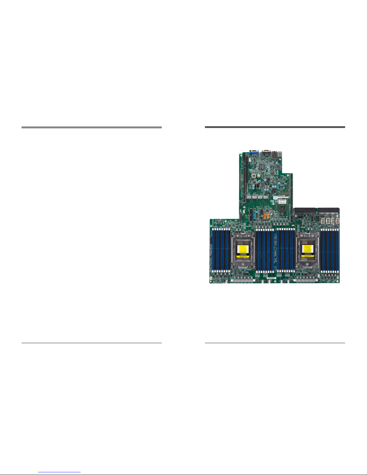
Figure 1-1. H11DSU-iN Motherboard Image
Note: All graphics shown in this manual were based upon the latest PCB revision available
at the time of publication of the manual. The motherboard you received may or may not look
exactly the same as the graphics shown in this manual.
Page 6
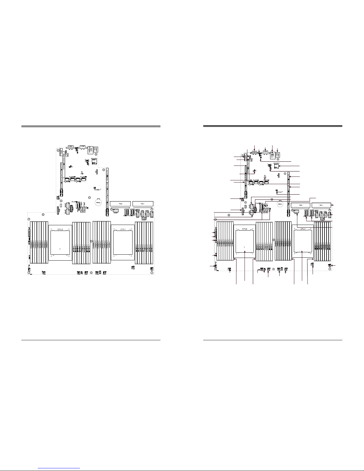
1110
Chapter 1: Introduction
H11DSU-iN User's Manual
H11DSU-i(N)
REV:1.01
JL1
JF1
FAN7
FAN8
JF2
P2-DIMMA1
P2-DIMMB1
P2-DIMMA2
P2-DIMMC1
P2-DIMMB2
P2-DIMMD2
P2-DIMMD1
P2-DIMMC2
JVR1
FAN3
FAN4
FAN5
FAN6
P2-DIMMH2
P2-DIMMG2
P2-DIMMH1
P2-DIMMF2
P2-DIMMG1
P2-DIMME2
P2-DIMMF1
P2-DIMME1
P1-DIMMD2
P1-DIMMC2
P1-DIMMC1
P1-DIMMD1
P1-DIMMA1
P1-DIMMA2
P1-DIMMB1
P1-DIMMB2
CPU1CPU2
P1-DIMMG1
P1-DIMMG2
P1-DIMMH1
P1-DIMMF2
P1-DIMMF1
P1-DIMME2
P1-DIMME1
P1-DIMMH2
FAN1
FAN2
JSGPIO
JGPW3
JUSB3
JTPM1
JSD2
SATA13
SATA12
JGPW2
JSD1
JBT1
Battery
P2_NVME0
P2_NVME1 P1_NVME1
P1_NVME0
JL2
J38
LEDM1
LE1
CPU1 PCI-E 3.0 x16 + CPU1 PCI-E 3.0 x16
CPU2 PCI-E 3.0 x16 + CPU2 PCI-E 3.0 x16
SXB3C
SXB1C
SXB1A
CPU1 PCIE 3.0 X8
PSU2 PSU1
LED1
JIPMB1
JLAN1
UID-LED
COM1
VGA
IPMI_LAN
USB0/1
(3.0)
JWD1JPG1
JSDCARD1
JPW4
JPW3JPW2
JPW1
JGPW1
SATA4~7SATA0~3
JS1: SATA8~11
JUSBA1
SXB2
CPU2 PCI-E 3.0 X16
JPB1
FAN8
JF1
FAN3
USB0/1
JPB1/JPG1/JWD1/
JL2
SGPIO
JIPMB1
SATA0~7
Figure 1-2. H11DSU-iN Motherboard Layout
H11DSU-i(N)
REV:1.01
JL1
JF1
FAN7
FAN8
JF2
P2-DIMMA1
P2-DIMMB1
P2-DIMMA2
P2-DIMMC1
P2-DIMMB2
P2-DIMMD2
P2-DIMMD1
P2-DIMMC2
JVR1
FAN3
FAN4
FAN5
FAN6
P2-DIMMH2
P2-DIMMG2
P2-DIMMH1
P2-DIMMF2
P2-DIMMG1
P2-DIMME2
P2-DIMMF1
P2-DIMME1
P1-DIMMD2
P1-DIMMC2
P1-DIMMC1
P1-DIMMD1
P1-DIMMA1
P1-DIMMA2
P1-DIMMB1
P1-DIMMB2
CPU1CPU2
P1-DIMMG1
P1-DIMMG2
P1-DIMMH1
P1-DIMMF2
P1-DIMMF1
P1-DIMME2
P1-DIMME1
P1-DIMMH2
FAN1
FAN2
JSGPIO
JGPW3
JUSB3
JTPM1
JSD2
SATA13
SATA12
JGPW2
JSD1
JBT1
Battery
P2_NVME0
P2_NVME1 P1_NVME1
P1_NVME0
JL2
J38
LEDM1
LE1
CPU1 PCI-E 3.0 x16 + CPU1 PCI-E 3.0 x16
CPU2 PCI-E 3.0 x16 + CPU2 PCI-E 3.0 x16
SXB3C
SXB1C
SXB1A
CPU1 PCIE 3.0 X8
PSU2 PSU1
LED1
JIPMB1
JLAN1
UID-LED
COM1
VGA
IPMI_LAN
USB0/1
(3.0)
JWD1JPG1
JSDCARD1
JPW4
JPW3JPW2
JPW1
JGPW1
SATA4~7SATA0~3
JS1: SATA8~11
JUSBA1
SXB2
CPU2 PCI-E 3.0 X16
JPB1
P2-DIMMA1~D2
BP
PWR1~4
GPU PWR3
JSDCARD1
IPMI LAN
SXB2
COM1
Notes:
• See Chapter 2 for detailed information on jumpers, I/O ports, and JF1 front panel
connections.
• Jumpers/LED indicators not indicated are used for testing only.
• Use only the correct type of onboard CMOS battery as specied by the manufacturer. Do
not install the onboard battery upside down to avoid possible explosion.
Quick Reference
VGA
SXB1A
SXB3B
SXB3A
JBR2
CPU1
JF2
JL1
FAN6
FAN2
FAN5
FAN4
FAN7
JVR1
FAN1
CPU2
JTPM1
NVMe Ports
GPU PWR2
USB3/4
JSD1/2
SATA12/13
GPU
PWR1
P2-DIMME1~H2
P1-DIMMA1~D2
P1-DIMME1~H2
LE1
LEDM1
LED1
JUIDB2 Switch and UID LED
JBT1
SXB1B
SATA8~11
PSU1/2
Page 7

1312
Chapter 1: Introduction
H11DSU-iN User's Manual
Quick Reference Table
Jumper Description Default Setting
J38 CPLD Code Programming NA
J39 Debug message through CPU UART0 NA
JBR2 Debug Mode for IPMI Use Pins 1-2 (Normal)
JBT1 CMOS Clear Open (Normal)
JPG1 VGA Enable/Disable Pins 1-2 (Enabled)
JVR1 VRM Code Programming Pin1: CLK, Pin2: DAT
JWD1 Watch Dog Pins 1-2 (Reset)
LED Description Status
LE1 Power LED Solid Green: Power On
LED1 UID LED Solid Blue: UID Switch On
LEDM1 BMC Heartbeat LED
Connector Description
BT1 Onboard Battery
COM1 COM Port
FAN1~FAN8 4-pin System/CPU Fan Headers
SATA0~13 SATA 3.0 Ports
SGPIO Serial Link General Purpose I/O Header
JF1 Front Control Panel Header 1
JF2 UltraIO Riser Card LAN LED Header
JIPMB1 System Management Bus Header
JL1 Chassis Intrusion Header
JLAN1 IPMI Gigabit LAN (RJ45) Port
GPU PWR1~3 12V 8-pin Power Connector for Riser Card GPU
BP PWR1~4 12V and 5V 8-pin Power Connector for Backplane
JSD1/JSD2 SATA DOM (Device on Module) power connectors 1/2
JSDCARD1 SD Card Port
JTPM1 Trusted Platform Module/Port 80 Connector
JUSBA1 USB 3.0 Type A Header
USB3 Front Panel USB3/4 3.0 ports
P1-NVME0/1 Processor 1 NVMe Ports
P2-NVME0/1 Processor 2 NVMe Ports
PSU1 Serverboard Main Power Supply Connector
PSU2 Serverboard Main Power Supply Connector
SXB1A/1B/1C WIO-L Riser Card Support (CPU1 PCI-E 3.0 x16 and CPU2 PCI-E 3.0 x16)
SXB2 WIO-R Riser Card Support (CPU2 PCI-E 3.0 x16)
SXB3A/3B/3C Ultra I/O Riser Card Support (CPU1 PCI-E 3.0 x 24, CPU2 PCI-E 3.0 x16)
USB0/1 Back panel Universal Serial Bus (USB) 3.0 Ports
Connector Description
VGA VGA Video Port
Note: Jumpers in the table not described are for manufacturing testing purposes only and
are not covered in this manual.
Page 8
1514
Chapter 1: Introduction
H11DSU-iN User's Manual
Note: The table above is continued on the next page.
Motherboard Features
Power Management
•
ACPI power management (S5)
• Power button override mechanism
• Power-on mode for AC power recovery
System Health Monitoring
•
Onboard voltage monitoring for +3.3V, +3.3V Standby, +5V, +5V Standby, +12V, VBAT, Memory, PCH Temp., System
Temp., Memory Temp.
• CPU switching phase voltage regulator
• CPU Thermal Trip support
• CPU Thermal Design Power (TDP) support of up to 180W (See Note 1 at the bottom)
Fan Control
•
Single cooling zone
• Low-noise fan speed control
• Pulse Width Modulation (PWM) fan control
System Management
•
Trusted Platform Module (TPM) support
• System resource alert via SuperDoctor® 5
• Power Supply Monitoring (JP1
2
C1)
• SuperDoctor® 5, Watch Dog
• Chassis intrusion header and detection (JL1)
• QA2, SUM-InBand, SUM-OOB, IPMICFG, IPMIVIew, SMCIPMITOOL
LED Indicators
•
CPU/Overheating
• Fan Failure
• HDD activity
• LAN activity
Dimensions
•
17" (L) x 16.8" (W) (431.8 mm x 426.72 mm)
Note 1: The CPU maximum thermal design power (TDP) is subject to chassis and heatsink
cooling restrictions. For proper thermal management, please check the chassis and heatsink
specications for proper CPU TDP sizing.
Motherboard Features
CPU
•
Dual EPYC 7000 series, processor in Socket SP3 sockets
Memory
•
Up to 4 TB of ECC DDR4 2400/2666 MHz speed, RDIMM/LRDIMM/3DS/NVDIMM memory in thirty-two (32) slots
DIMM Size
• Up to 128 GB size at 1.2V
Chipset
•
System on Chip
Expansion Slots
WIO:
• 1 x PCI-E 3.0 x32
• 1 x PCI-E 3.0 x16
Ultra:
• 1 x PCI-E 3.0 x40
Network
•
ATEN IPMI from ASPEED BMC for gigabit RJ45 port
Graphics
•
ASPEED AST2500 BMC chip with one (1) VGA port
I/O Devices
•
COM Port • One (1) COM connector on rear I/O panel
• SATA/NVMe Ports
• Fourteen (14) SATA 3.0 ports (SATA0~13)
• Two (2) SATA-DOM ports
• Four (4) internal NVMe ports
Peripheral Devices
•
Two (2) USB 3.0 ports on the rear I/O panel (USB0/1)
• One (1) USB 3.0 Type A connector for front access (USB2)
• One (1) USB 3.0 header for front control panel (USB3/4)
BIOS
•
128Mb SPI AMI BIOS® SM Flash UEFI BIOS
• ACPI 5.1, SMBIOS 3.1.1, Plug-and-Play (PnP), BIOS rescue hot-key, RTC (Real Time Clock) wakeup, Riser Card Auto-
Detection Support
Motherboard Features
Page 9
1716
Chapter 1: Introduction
H11DSU-iN User's Manual
Note: This is a general block diagram and may not exactly represent the features on your
motherboard. See the previous pages for the actual specications of your motherboard.
Figure 1-3.
System Block Diagram
1.2 Processor and Chipset Overview
Built upon the functionality and capability of the EPYC 7000 series processor in an Socket SP3
socket and a System on Chip chipset. The H11DSU-iN motherboard offers maximum I/O
expendability, energy efciency, and data reliability in a 14-nm process architecture, and
is optimized for embedded storage solutions, networking applications, or cloud-computing
platforms.
With support of the new microarchitecture 14 nm process technology, the H11DSU-iN
drastically increases system performance for a multitude of server applications.
The EPYC 7000 series supports the following features:
• ACPI Power Management Logic Support Rev. 6.1
• Adaptive Ther mal Management/Monitor ing
• PCI -E 3.0, SATA 3.0 w/transfer rates of up to 6 Gb/s
• System Management Bus (SMBus) Specic ation Version 2.0
1.3 Special Features
This section describes the health monitoring features of the H11DSU-iN motherboard. The
motherboard has an onboard System Hardware Monitor chip that supports system health
monitoring.
Recovery from AC Power Loss
The Basic I/O System (BIOS) provides a setting that determines how the system will respond
when AC power is lost and then restored to the system. You can choose for the system to
remain powered off (in which case you must press the power switch to turn it back on), or
for it to automatically return to the power-on state. See the Advanced BIOS Setup section
for this setting. The default setting is Last State.
5
5
4
4
3
3
2
2
1
1
D D
C C
B B
A A
H11DSU-iN
AMD SP3 Rev. 1.02
CPU 1
A
DDR4 DIMM
#1
#2
E
CPU 2
NVMe x4
I- PASS SATA x4
I- PASS SATA x4
NVMe x4
NVMe x4
NVMe x4
CPU1 P0 [15:8]CPU2 P0 [15:8]
BMC
AST2500
CPU1 P0 [0]
CPU1 P1 [7:0]
CPU1 USB
Rear USB
X 2
CPU1 P0 [2]
VGA COM
IPMI LAN
RJ45
PHY
RTL8211F
DDR4
LPC
BMC ROM
32MB
TPM
BIOS ROM
32MB
MUX
SPI
SPI
DDR4 DIMM
#1
#2
DDR4 DIMM
#1
#2
DDR4 DIMM
#1
#2
DDR4 DIMM
#1
#2
DDR4 DIMM
#1
#2
DDR4 DIMM
#1
#2
DDR4 DIMM
#1
#2
DDR4 DIMM
#1
#2
DDR4 DIMM
#1
#2
DDR4 DIMM
#1
#2
DDR4 DIMM
#1
#2
DDR4 DIMM
#1
#2
DDR4 DIMM
#1
#2
DDR4 DIMM
#1
#2
DDR4 DIMM
#1
#2
B
C
D
F
G
H
E
H
G
F
A
B
C
D
NIC
Port A
0~7
Port A NCSI Port B
Port B
0~15
Port C
Port C
0~15
CPU1 P1 [15:8]
CPU1 P3 [15:0]
NCSI
Port 1
0 ~ 15
Port 2
0 ~ 15
Ultra IO
WIO-L
WIO-R
CPU2 P2 [15:0]
0 ~ 15
CPU2 P3 [15:0] CPU1 P2 [15:0]CPU2 P1 [15:0]
SATA DOM
SATA DOM
CPU2 P0 [3:2]
USB3
CTRL
Micro SD
I- PASS SATA x4
CPU2 P0 [7:4]
TYPE-A x1
CPU1 USB
USB3
CTRL
USB3 HDR x2
CPU1 P0 [4]
Title
Size Document Number Rev
Date: Sheet
of
UPER
S
®
980 Rock Ave., San Jose CA, 95131
TEL : (408) 503-8000
CONFIDENTIAL - DO NOT DUPLICATE
H11DSU-iN
1.00
<Title>
Custom
1 115
<Variant Name>
Title
Size Document Number Rev
Date: Sheet
of
UPER
S
®
980 Rock Ave., San Jose CA, 95131
TEL : (408) 503-8000
CONFIDENTIAL - DO NOT DUPLICATE
H11DSU-iN
1.00
<Title>
Custom
1 115
<Variant Name>
Title
Size Document Number Rev
Date: Sheet
of
UPER
S
®
980 Rock Ave., San Jose CA, 95131
TEL : (408) 503-8000
CONFIDENTIAL - DO NOT DUPLICATE
H11DSU-iN
1.00
<Title>
Custom
1 115
<Variant Name>
Page 10

1918
Chapter 1: Introduction
H11DSU-iN User's Manual
1.4 System Health Monitoring
This section describes the health monitoring features of the H11DSU-iN motherboard. The
motherboard has an onboard chip that supports system health monitoring. Once a voltage
becomes unstable, a warning is given or an error message is sent to the screen. The user
can adjust the voltage thresholds to dene the sensitivity of the voltage monitor.
Onboard Voltage Monitors
The onboard voltage monitor will continuously scan crucial voltage levels. Once a voltage
becomes unstable, it will give a warning or send an error message to the screen. Users can
adjust the voltage thresholds to dene the sensitivity of the voltage monitor. Real time readings
of these voltage levels are all displayed in BMC.
Fan Status Monitor with Firmware Control
PC health monitoring in the BIOS can check the RPM status of the cooling fans. The onboard
CPU and chassis fans are controlled by Thermal Management.
Environmental Temperature Control
The thermal control sensor monitors the CPU temperature in real time and will turn on the
thermal control fan whenever the CPU temperature exceeds a user-dened threshold. The
overheat circuitry runs independently from the CPU. Once the thermal sensor detects that
the CPU temperature is too high, it will automatically turn on the thermal fans to prevent the
CPU from overheating. The onboard chassis thermal circuitry can monitor the overall system
temperature and alert the user when the chassis temperature is too high.
Note: To avoid possible system overheating, please be sure to provide adequate airow to
your system.
System Resource Alert
This feature is available when used with SuperDoctor 5®. SuperDoctor 5 is used to notify the
user of certain system events. For example, you can congure SuperDoctor 5 to provide you
with warnings when the system temperature, CPU temperatures, voltages and fan speeds
go beyond a predened range.
1.5 ACPI Features
ACPI stands for Advanced Conguration and Power Interface. The ACPI specication denes
a exible and abstract hardware interface that provides a standard way to integrate power
management features throughout a computer system including its hardware, operating system
and application software. This enables the system to automatically turn on and off peripherals
such as network cards, hard disk drives and printers.
In addition to enabling operating system-directed power management, ACPI also provides a
generic system event mechanism for Plug and Play and an operating system-independent
interface for conguration control. ACPI leverages the Plug and Play BIOS data structures
while providing a processor architecture-independent implementation that is compatible with
Windows 8/R2 and Windows 2012/R2 operating systems.
1.6 Power Supply
As with all computer products, a stable power source is necessary for proper and reliable
operation. It is even more important for processors that have high CPU clock rates. In areas
where noisy power transmission is present, you may choose to install a line lter to shield
the computer from noise. It is recommended that you also install a power surge protector to
help avoid problems caused by power surges.
1.7 Super I/O
The Super I/O (Aspeed AST2500 chip) includes a data separator, write pre-compensation
circuitry, decode logic, data rate selection, a clock generator, drive interface control logic and
interrupt and DMA logic. The wide range of functions integrated onto the Super I/O greatly
reduces the number of components required for interfacing with oppy disk drives.
The Super I/O provides one high-speed, 16550 compatible serial communication port
(UART), which supports serial infrared communication. This UART includes a 16-byte send/
receive FIFO, a programmable baud rate generator, complete modem control capability and
a processor interrupt system. This UART provides legacy speed with baud rate of up to
115.2 Kbps as well as an advanced speed with baud rates of 250 K, 500 K, or 1 Mb/s, which
support higher speed modems.
The Super I/O provides functions that comply with ACPI (Advanced Conguration and Power
Interface), which includes support of legacy and ACPI power management through a SMI
or SCI function pin. It also features auto power management to reduce power consumption.
The IRQs, DMAs and I/O space resources of the Super I/O can be exibly adjusted to meet
ISA PnP requirements, which support ACPI and APM (Advanced Power Management).
Page 11

2120
Chapter 2: InstallationH11DSU-iN User's Manual
Chapter 2
Installation
2.1 Static-Sensitive Devices
Electrostatic Discharge (ESD) can damage electronic com ponents. To prevent damage to your
motherboard, it is important to handle it very carefully. The following measures are generally
sufcient to protect your equipment from ESD.
Precautions
•
Use a grounded wrist strap designed to prevent static discharge.
• Touch a grounded metal object before removing the board from the antistatic bag.
• Handle the board by its edges only; do not touch its components, peripheral chips, memory
modules or gold contacts.
• When handling chips or modules, avoid touching their pins.
• Put the motherboard and peripherals back into their antistatic bags when not in use.
• For grounding purposes, make sure that your chassis provides excellent conductivity be-
tween the power supply, the case, the mounting fasteners and the motherboard.
• Use only the correct type of CMOS onboard battery as specied by the manufacturer. Do
not install the CMOS battery upside down, which may result in a possible explosion.
Unpacking
The motherboard is shipped in antistatic packaging to avoid static damage. When unpacking
the motherboard, make sure that the person handling it is static protected.
2.2 Motherboard Installation
All motherboards have standard mounting holes to t different types of chassis. Make sure
that the locations of all the mounting holes for both the motherboard and the chassis match.
Although a chassis may have both plastic and metal mounting fasteners, metal ones are
highly recommended because they ground the motherboard to the chassis. Make sure that
the metal standoffs click in or are screwed in tightly.
Philips
Screwdriver (1)
Standoffs (13)
Only if Needed
Philips Screws (13)
Tools Needed
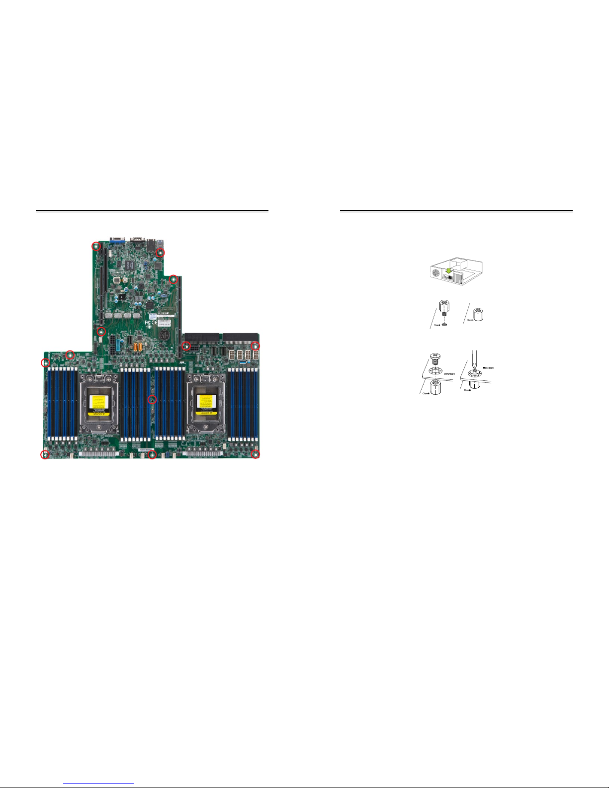
Location of Mounting Holes
Notes:
1. To avoid damaging the motherboard and its components, please do not use a force
greater than 8 lb/inch on each mounting screw during motherboard installation.
2. Some components are very close to the mounting holes. Please take precautionary
measures to avoid damaging these components when installing the motherboard to the
chassis.
Page 12
2322
Chapter 2: InstallationH11DSU-iN User's Manual
Figure 2-1. Motherboard Mounting Holes
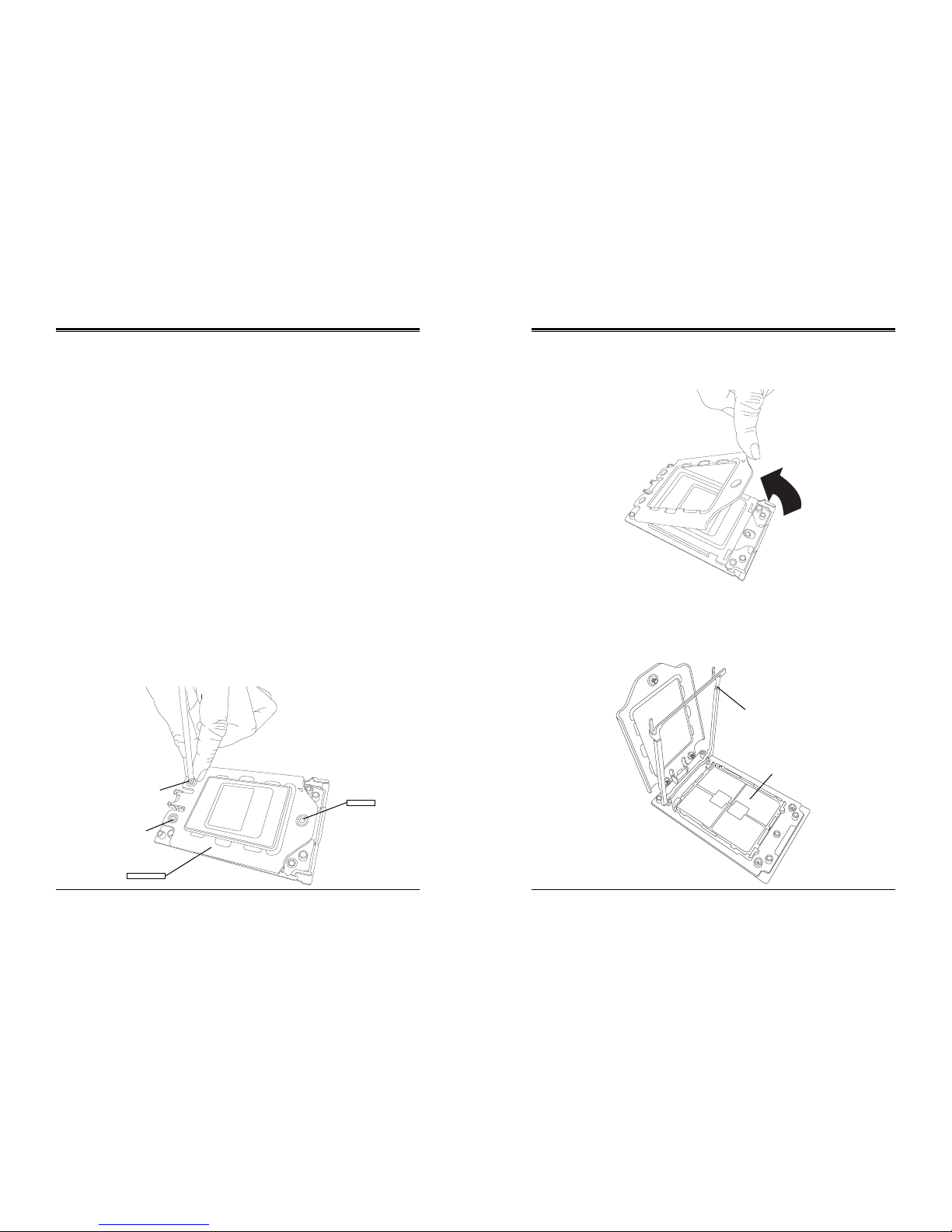
Installing the Motherboard
1. Install the I/O shield into the back of the chassis.
2. Locate the mounting holes on the motherboard. See the previous page for the location.
3. Locate the matching mounting holes on the chassis. Align the mounting holes on the
motherboard against the mounting holes on the chassis.
4. Install standoffs in the chassis as needed.
5. Install the motherboard into the chassis carefully to avoid damaging other motherboard
components.
6. Using the Phillips screwdriver, insert a Phillips head #6 screw into a mounting hole on
the motherboard and its matching mounting hole on the chassis.
7. Repeat Step 5 to insert #6 screws into all mounting holes.
8. Make sure that the motherboard is securely placed in the chassis.
Note: Images displayed are for illustration only. Your chassis or components might look
different from those shown in this manual.
Page 13
2524
Chapter 2: InstallationH11DSU-iN User's Manual
2.3 Processor and Heatsink Installation
Warning: When handling the processor package, avoid placing direct pressure on the label
area of the fan.
Important:
• For the Processor/Heatsink installation you need to use a T20 screwdriver when opening/
closing the CPU socket.
• Always connect the power cord last, and always remove it before adding, removing or
changing any hardware components. Make sure that you install the processor into the
CPU socket before you install the CPU heatsink.
• If you buy a CPU separately, make sure that you use an Intel-certied multi-directional
heatsink only.
• Make sure to install the motherboard into the chassis before you install the CPU heatsink.
• When receiving a motherboard without a processor pre-installed, make sure that the plastic
CPU socket cap is in place and none of the socket pins are bent; otherwise, contact your
retailer immediately.
• Refer to the Supermicro website for updates on CPU support.
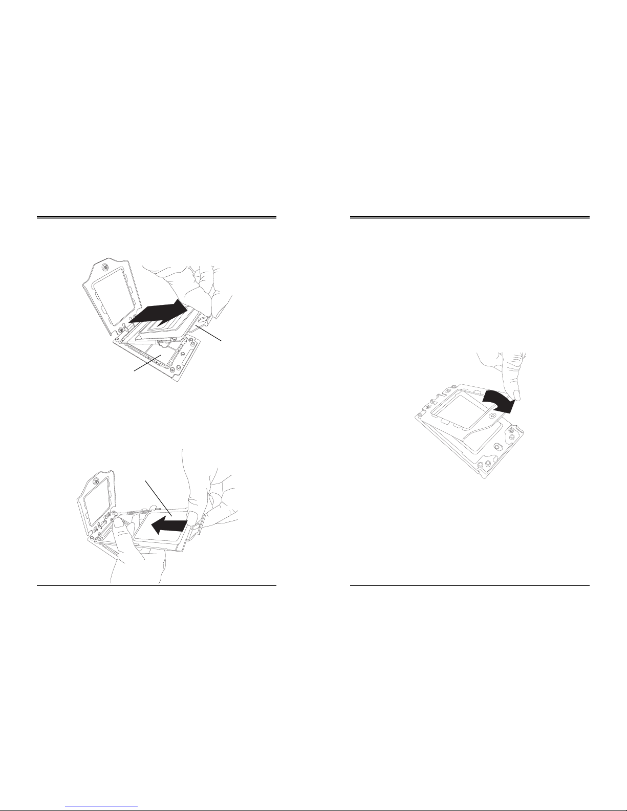
Installing the Processor and Heatsink
1. Unscrew the screws holding down Force Frame in the sequence of 3-2-1. The screws
are numbered on the Force Frame next to each screw hole.
Screw #1
Screw #2
Screw #3
Force Frame
2. The spring-loaded Force Frame will raise up after the last screw securing it (#1) is
removed. Gently allow it to lift up to its stopping position.
3. Lift the Rail Frame up by gripping the lift tabs near the front end of the rail frame. While
keeping a secure grip of the Rail Frame, lift it to a position so you can do the next step
of removing the External Cap.
Note: The Rail Frame is spring loaded, so keep a secure grip on it as you lift it so it does
not snap up.
Rail Frame
PnP Cover Cap
Page 14
2726
Chapter 2: InstallationH11DSU-iN User's Manual
4. Remove the External Cap from the Rail Frame by pulling it upwards through the rail
guides on the Rail Frame.
External Cap
5. The CPU Package is shipped from the factory with the blue Carrier Frame preassembled. Grip the handle of the Carrier Frame/CPU Package assembly from its
shipping tray, and while gripping the handle, align the anges of the Carrier Frame
onto the rails of the Rail Frame so its pins will be at the bottom when the Rail Frame is
lowered later.
6. Slide the Carrier Frame/CPU Package downwards to the bottom of the Rail Frame.
Ensure the anges are secure on the rails as you lower it downwards.
Carrier Frame/
CPU Package
PnP Cover Cap
Note: You can only install the CPU inside the socket in one direction with the handle at the
top. Make sure that it is properly inserted into the CPU socket before closing the Rail Frame
plate. If it doesn't close properly, do not force it as it may damage your CPU. Instead, open
the Rail Frame plate again, and double-check that the CPU is aligned properly.
7. Lift up the Rail Frame till it securely rests in upright position. Then remove the PnP
Cover Cap from the CPU socket below. Grip the two lift tabs marked "Remove" at the
middle of the cap and pull vertically upwards to remove the PnP Cover Cap.
Warning! The exposed socket contacts are extremely vulnerable and can be damaged easily.
Do not touch or drop objects onto the contacts and be careful removing the PnP Cover Cap
and when placing the Rail Frame over the socket.
8. Gently lower the Rail Frame down onto the socket until the latches on the Rail Frame
engage with the Socket housing. and it rests in place. DO NOT force it into place!
Page 15
2928
Chapter 2: InstallationH11DSU-iN User's Manual
9. Gently lower the Force Frame down onto the Rail Frame and hold it in place until it is
seated in the Socket housing. Note that the Force Frame is spring loaded and has to be
held in place before it is secured.
10. Place and re-screw the screws in the reverse order to the way you removed them
(holes 1-2-3 in order). When nished, the Force Frame will be secure over both the Rail
Frame and CPU Package.
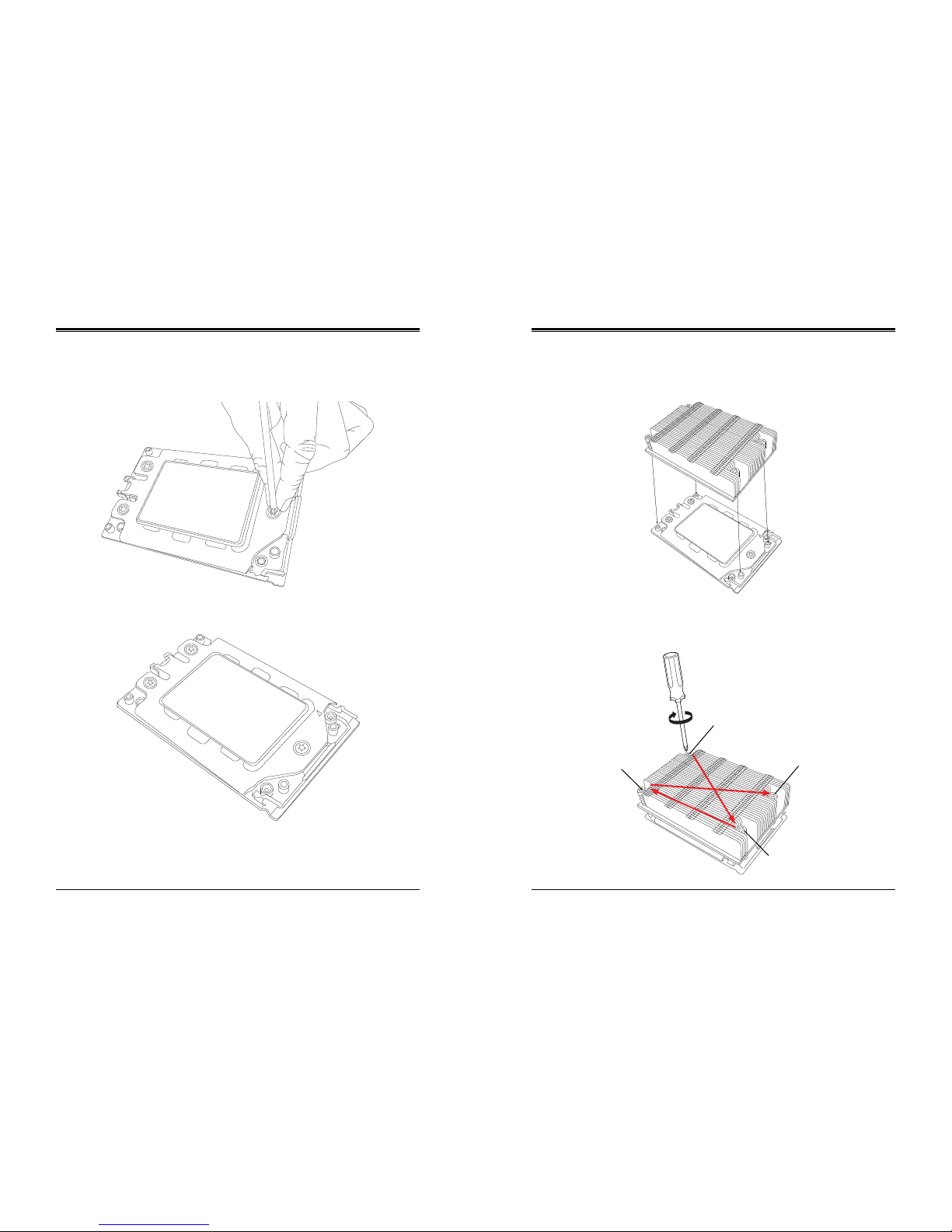
11. After the Force Frame is secured and the CPU package is in place, now you must
install the heatsink to the frame. Lower the heatsink down till it rests securely over the
four screw holes on CPU Package on the socket frame.
12. Using a diagonal pattern, tighten the four screws down on the heatsink in a clockwise
fashion till it is secure. The heatsink will now be secured and you have nished installing
the processor and heatsink onto the motherboard. Repeat this procedure for any
remaining CPU sockets on the Motherboard.
#1 Screw
#2 Screw
#3 Screw
#4 Screw
Page 16
3130
Chapter 2: InstallationH11DSU-iN User's Manual
Un-installing the Processor and Heatsink
1. Remove the heatsink attached to the top of the CPU Package by reversing the
installation procedure.
2. Clean the Thermal grease left by the heatsink on the CPU package lid to limit the risk of
it contaminating the CPU package land pads or contacts in the socket housing.
3. Reverse the procedure for installing the Force Frame onto the socket, unscrewing the
plate in the 3-2-1 screw order and lift the Force Frame to the vertical position.
4. Lift the Rail Frame using the lift tabs near the front end of the Rail Frame. Note that the
Rail Frame is spring loaded, so be careful lifting it up into a vertical position.
5. Grip the handle of the Carrier Frame and pull upwards to extract it from the Rail Frame.
Return the Carrier Frame/CPU Package to its original shipping container.
6. Grip the handle on the External Cap and return it to the Rail Frame sliding it downwards
till it rests in the frame.
7. Gripping the Rail Frame, rotate it downwards till it rests above and locks over the socket
housing in its horizontal position.
8. Push and rotate down the Force Frame till it is over the External Cap and Rail Frame
into a horizontal position.
9. While holding down the Force Frame, secure it back to the socket frame by securing
screw 1 in place. Note that without a CPU Package in place, it is not necessary to
tighten down screws 2 and 3 at this time.
Memory Support and Installation
Note: Check the Supermicro website for recommended memory modules.
Important: Exercise extreme care when installing or removing DIMM modules to prevent
any possible damage.
Memory Support
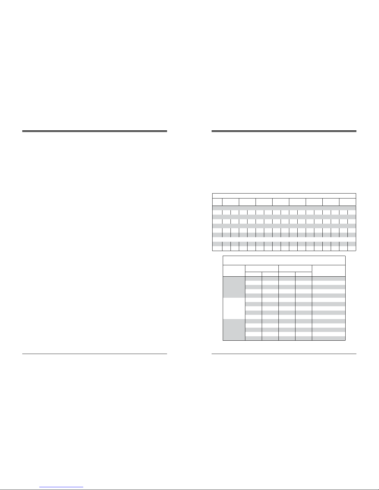
The H11DSU-iN supports Up to 4 TB of ECC DDR4 2400/2666 MHz speed, RDIMM/
LRDIMM/3DS/NVDIMM memory in thirty-two (32) slots. Refer to the table below for additional
memory information.
Processors and their Corresponding Memory Modules
CPU#
Channel 1Channel 2Channel 3Channel 4Channel 5Channel 6Channel 7Channel
8
8 DIMMS
CPU1
A2 B2 C2 D2 E2 F2 G2 H2
16 DIMMS
CPU1
A1 A2 B1 B2 C1 C2 D1 D2 E1 E2 F1 F2 G1 G2 H1 H2
16 DIMMS
CPU1
A2 B2 C2 D2 E2 F2 G2 H2
CPU2
A2 B2 C2 D2 E2 F2 G2 H2
32 DIMMS
CPU1
A1 A2 B1 B2 C1 C2 D1 D2 E1 E2 F1 F2 G1 G2 H1 H2
CPU2
A1 A2 B1 B2 C1 C2 D1 D2 E1 E2 F1 F2 G1 G2 H1 H2
Populating RDIMM/RDIMM 3DS/LRDIMM/LRDIMM 3DS DDR4 Memory
Modules
Type
DIMM Population
Maximum DIMM
Capacity (GB)
Maximum Frequency
(MHz)
DIMM1 DIMM2 1 Channel 8 Channel
RDIMM
1R 16GB 128GB 2666
1R 1R 32GB 256GB 2133
2R 32GB 256GB 2400
1R 2R 48GB 384GB 1866
2R 2R 64GB 512GB 2133
LRDIMM
4R 64GB 512GB 2666
4R 4R 128GB 1TB 2133
8R 128GB 1TB 2666
4R 8R 192GB 1.5TB 2133
8R 8R 256GB 2TB 2133
LRDIMM 3DS
2R2H 64GB 512GB 2400
2R2H 2R2H 128GB 1TB 1866
2R4H 128GB 1TB 2400
2R2H 2R4H 192GB 1.5TB 1866
2R4H 2R4H 256GB 2TB 1866
Page 17

3332
Chapter 2: InstallationH11DSU-iN User's Manual
DIMM Module Population Sequence
When installing memory modules, the DIMM slots should be populated in the following order:
DIMMA2, DIMMB2, DIMMC2, DIMMD2, DIMME2, DIMMF2, DIMMG2, DIMMH2, then
DIMMA1, DIMMB1, DIMMC1, DIMMD1, DIMME1, DIMMF1, DIMMG1, DIMMH1.
• The blue slots must be populated rst.
• Always use DDR4 DIMM modules of the same type, size and speed.
• Mixed DIMM speeds can be installed. However, all DIMMs will run at the speed of the
slowest DIMM.
• The motherboard will support odd-numbered modules (1 or 3 modules installed). However,
to achieve the best memory performance, a balanced memory population is recommended.
Figure 2-2. DIMM Numbering
P2-DIMMA1
P2-DIMMA2
P2-DIMMB1
P2-DIMMB2
P2-DIMMC1
P2-DIMMC2
P2-DIMMD1
P2-DIMMD2
P2-DIMMH2
P2-DIMMH1
P2-DIMMG2
P2-DIMMG1
P2-DIMMF2
P2-DIMMF1
P2-DIMME2
P2-DIMME1
P1-DIMMA1
P1-DIMMA2
P1-DIMMB1
P1-DIMMB2
P1-DIMMC1
P1-DIMMC2
P1-DIMMD1
P1-DIMMD2
P1-DIMMH2
P1-DIMMH1
P1-DIMMG2
P1-DIMMG1
P1-DIMMF2
P1-DIMMF1
P1-DIMME2
P1-DIMME1
DIMM Installation
1. Insert the desired number of DIMMs into
the memory slots, starting with DIMMA2,
DIMMB2, DIMMC2, DIMMD2, DIMME2,
DIMMF2, DIMMG2, DIMMH2, then
DIMMA1, DIMMB1, DIMMC1, DIMMD1,
DIMME1, DIMMF1, DIMMG1, DIMMH1.
For best performance, please use the
memory modules of the same type and
speed.
2. Push the release tabs outwards on both
ends of the DIMM slot to unlock it.
3. Align the key of the DIMM module with
the receptive point on the memory slot.
4. Align the notches on both ends of the
module against the receptive points on
the ends of the slot.
5. Press the notches on both ends of the
module straight down into the slot until
the module snaps into place.
6. Press the release tabs to the lock
positions to secure the DIMM module
into the slot.
DIMM Removal
Press both release tabs on the ends of the
DIMM module to unlock it. Once the DIMM
module is loosened, remove it from the
memory slot.
Release Tabs
Notches
Press both notches
straight down into
the memory slot.
Page 18

3534
Chapter 2: InstallationH11DSU-iN User's Manual
H11DSU-i(N)
REV:1.01
JL1
JF1
FAN7
FAN8
JF2
P2-DIMMA1
P2-DIMMB1
P2-DIMMA2
P2-DIMMC1
P2-DIMMB2
P2-DIMMD2
P2-DIMMD1
P2-DIMMC2
JVR1
FAN3
FAN4
FAN5
FAN6
P2-DIMMH2
P2-DIMMG2
P2-DIMMH1
P2-DIMMF2
P2-DIMMG1
P2-DIMME2
P2-DIMMF1
P2-DIMME1
P1-DIMMD2
P1-DIMMC2
P1-DIMMC1
P1-DIMMD1
P1-DIMMA1
P1-DIMMA2
P1-DIMMB1
P1-DIMMB2
CPU1CPU2
P1-DIMMG1
P1-DIMMG2
P1-DIMMH1
P1-DIMMF2
P1-DIMMF1
P1-DIMME2
P1-DIMME1
P1-DIMMH2
FAN1
FAN2
JSGPIO
JGPW3
JUSB3
JTPM1
JSD2
SATA13
SATA12
JGPW2
JSD1
JBT1
Battery
P2_NVME0
P2_NVME1 P1_NVME1
P1_NVME0
JL2
J38
LEDM1
LE1
CPU1 PCI-E 3.0 x16 + CPU1 PCI-E 3.0 x16
CPU2 PCI-E 3.0 x16 + CPU2 PCI-E 3.0 x16
SXB3C
SXB1C
SXB1A
CPU1 PCIE 3.0 X8
PSU2 PSU1
LED1
JIPMB1
JLAN1
UID-LED
COM1
VGA
IPMI_LAN
USB0/1
(3.0)
JWD1JPG1
JSDCARD1
JPW4
JPW3JPW2
JPW1
JGPW1
SATA4~7SATA0~3
JS1: SATA8~11
JUSBA1
SXB2
CPU2 PCI-E 3.0 X16
JPB1
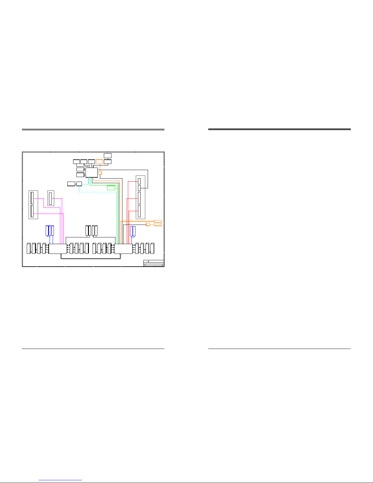
2.5 Rear I/O Ports
See Figure 2-1 below for the locations and descriptions of the various I/O ports on the rear
of the motherboard.
Figure 2-3. I/O Port Locations and Denitions
Rear I/O Ports
# Description # Description
1. USB 0/1 Ports 4. UID LED
2. IPMI LAN Port 5. VGA Port
3 COM1 Port
1 5432
COM Ports
One COM port (COM1) on the rear I/O panel.
IPMI LAN Port
One IPMI LAN port is located on the I/O back panel. This port accepts an RJ45 type cable.
Universal Serial Bus (USB) Ports
There are two USB 3.0 ports (USB0/1) on the I/O back panel. The motherboard also provides
two USB 3.0 connections via USB headers (USB3/4). The JUSBA1 header is USB Type A. The
onboard headers can be used to provide front side USB access with a cable (not included).
Back Panel USB 3.0 (USB0/1)
Pin Denitions
Pin# Denition Pin# Denition
1 VBUS 10 Power
2 D- 11 USB 2.0 Differential Pair
3 D+ 12
4 Ground 13 Ground of PWR Return
5 StdA_SSRX- 14 SuperSpeed Receiver
6 StdA_SSRX+ 15 Differential Pair
7 GND_DRAIN 16 Ground for Signal Return
8 StdA_SSTX- 17 SuperSpeed Transmitter
9 StdA_SSTX+ 18 Differential Pair
Back Panel USB 3.0 (USB3/4)
Pin Denitions
Pin# Denition Pin# Denition
1 USB30_Front_VCC
2 USB3_HDR0_SSRX_L_CHK 19 USB30_Front_VCC
3 USB3_HDR0_SSRX_H_CHK 18 USB3_HDR1_SSRX_L_CHK
4 GND 17 USB3_HDR1_SSRX_H_CHK
5 USB3_HDR0_SSTX_L_CHK 16 GND
6 USB3_HDR0_SSTX_H_CHK 15 USB3_HDR1_SSTX_L_CHK
7 GND 14 USB3_HDR1_SSTX_H_CHK
8 USB3_HDR0_D_L 13 GND
9 USB3_HDR0_D_H 12 USB3_HDR1_D_L
10 GND 11 USB3_HDR1_D_H
Front Panel USB 3.0 (JUSBA1)
Header Pin Denitions
Pin# Denition Pin# Denition
12 CG 13 CG
1 VBUS 5 Stda_SSRX-N
2 D-N 6 Stda_SSRX-P
3 D-P 7 GND_DRAIN
4 GND 8 Stda_SSTX_N
9 Stda_SSTX-P
10 CG 11 CG
VGA Port
A video (VGA) port is located next to JLAN1 on the I/O back panel. Refer to the board layout
below for the location.
Page 19

3736
Chapter 2: InstallationH11DSU-iN User's Manual
H11DSU-i(N)
REV:1.01
JL1
JF1
FAN7
FAN8
JF2
P2-DIMMA1
P2-DIMMB1
P2-DIMMA2
P2-DIMMC1
P2-DIMMB2
P2-DIMMD2
P2-DIMMD1
P2-DIMMC2
FAN3
FAN4
FAN5
FAN6
P2-DIMMH2
P2-DIMMG2
P2-DIMMH1
P2-DIMMF2
P2-DIMMG1
P2-DIMME2
P2-DIMMF1
P2-DIMME1
P1-DIMMD2
P1-DIMMC2
P1-DIMMC1
P1-DIMMD1
P1-DIMMA1
P1-DIMMA2
P1-DIMMB1
P1-DIMMB2
CPU1CPU2
P1-DIMMG1
P1-DIMMG2
P1-DIMMH1
P1-DIMMF2
P1-DIMMF1
P1-DIMME2
P1-DIMME1
P1-DIMMH2
FAN1
FAN2
JSGPIO
JGPW3
JUSB3
JTPM1
JSD2
SATA13
SATA12
JGPW2
JSD1
JBT1
Battery
P2_NVME0
P2_NVME1 P1_NVME1
P1_NVME0
JL2
J38
LEDM1
LE1
CPU1 PCI-E 3.0 x16 + CPU1 PCI-E 3.0 x16
CPU2 PCI-E 3.0 x16 + CPU2 PCI-E 3.0 x16
SXB3C
SXB1C
SXB1A
CPU1 PCIE 3.0 X8
PSU2 PSU1
LED1
JIPMB1
JLAN1
UID-LED
COM1
VGA
IPMI_LAN
USB0/1
(3.0)
JWD1JPG1
JSDCARD1
JPW4
JPW3JPW2
JPW1
JGPW1
SATA4~7SATA0~3
JS1: SATA8~11
JUSBA1
SXB2
CPU2 PCI-E 3.0 X16
JPB1
Figure 2-4. JF1 Header Pins
2.6 Front Control Panel
JF1 contains header pins for various buttons and indicators that are normally located on a
control panel at the front of the chassis. These connectors are designed specically for use
with Supermicro chassis. See the gure below for the descriptions of the front control panel
buttons and LED indicators.
NMI (Control signal)
Key
(5V standby)
(Vcc)
(Vcc)
(Vcc)
(Vcc)
(Vcc)
Reset Button (Data signal)
Power Button (Data signal)
(Ground)
Key
Power On LED (Control signal)
HDD LED (Activity signal)
NIC1 LED (Ground)
NIC2 LED (Ground)
UID LED (Ground)
Power Fail LED (Ground)
(Ground)
(Ground)
2 1
20 19
Power Button
The Power Button connection is located on pins 1 and 2 of JF1. Momentarily contacting both
pins will power on/off the system. This button can also be congured to function as a suspend
button (with a setting in the BIOS - see Chapter 4). To turn off the power in the suspend
mode, press the button for at least 4 seconds. Refer to the table below for pin denitions.
Power Button
Pin Denitions (JF1)
Pin# Denition
1 Signal
2 Ground
Reset Button
The Reset Button connection is located on pins 3 and 4 of JF1. Attach it to a hardware reset
switch on the computer case to reset the system. Refer to the table below for pin denitions.
Reset Button
Pin Denitions (JF1)
Pin# Denition
3 Reset
4 Ground
Power Fail LED
The Power Fail LED connection is located on pins 5 and 6 of JF1.
Power Fail LED
Pin Denitions (JF1)
Pin# Denition
5 3.3V
6 PWR Supply Fail
Page 20

3938
Chapter 2: InstallationH11DSU-iN User's Manual
NIC1/NIC2 (LAN1/LAN2)
The NIC (Network Interface Controller) LED connection for LAN port 1 is located on pins 11
and 12 of JF1, and the LED connection for LAN Port 2 is on Pins 9 and 10. Attach the NIC
LED cables here to display network activity.
LAN1/LAN2 LED
Pin Denitions (JF1)
Pin# Denition
9 NIC2 Activity LED
10 NIC2 Link LED
11 NIC1 Activity LED
12
NIC1 Link LED
HDD LED/UID Switch
The HDD LED/UID Switch connection is located on pins 13 and 14 of JF1. Attach a cable to
Pin 14 to show hard drive activity status. Attach a cable to Pin 13 to use UID switch. Refer
to the table below for pin denitions.
HDD LED
Pin Denitions (JF1)
Pin# Denition
13 3.3V Standby/UID Switch
14 HDD Active
Unit Identier Switch/UID LED Indicator
A Unit Identier (UID) switch is located on the I/O backplane, and two UID LED indicators are
located on the serverboard. The rear UID LED (LED1) is located next to the UID switch. The
front UID LED is located on pins 7 & 8 on the front control panel (JF1). When you press the
UID switch, both rear and front UID LED indicators will be turned on. Press the UID switch
again to turn off the LED indicators. The UID Indicators provide easy identication of a system
unit that may be in need of service.
Note: UID can also be triggered via IPMI on the serverboard. For more information on IPMI,
please refer to the IPMI User's Guide posted on our website @ http://www.supermicro.com.
UID Switch
Pin# Denition
1 Ground
2 Ground
3 Button In
4 Button Out
UID LED
Status
Color/State Status
Blue: On Unit Identied
Power LED
The Power LED connection is located on pins 15 and 16 of JF1.
Power LED
Pin Denitions (JF1)
Pin# Denition
15 3.3V
16 Power LED
NMI Button
The non-maskable interrupt button header is located on pins 19 and 20 of JF1.
NMI Button
Pin Denitions (JF1)
Pin# Denition
19 Control
20 Ground
2.7 Connectors
Power Connections
PSU1/PSU2 Main Power Supply Connectors
The primary power supply connectors (PSU1/PSU2) are proprietary power connectors that
the power supply plugs into directly.
Backplane 12V and 5V 8-pin Power Connectors
BP PWR1/BP PWR2/BP PWR3/BP PWR4 are 8-pin 12V and 5V DC power inputs for the
system's backplane. Refer to the table below for pin denitions.
Backplane 8-pin Power
Pin Denitions
Pin# Denition
1 - 4 Ground
5 - 6 +12V
7 - 8 +5V
GPU 12V 8-pin Power Connectors
GPU PWR1/GPU PWR2/GPU PWR3 are 8-pin 12V DC power inputs for GPUs that are
installed in the system's PCI-E slots. Refer to the table below for pin denitions.
GPU 8-pin Power
Pin Denitions
Pin# Denition
1 - 4 Ground
5 - 8 +12V
Page 21

4140
Chapter 2: InstallationH11DSU-iN User's Manual
Fan Headers
There are eight fan headers on the motherboard. These are 4-pin fan headers; pins 1-3
are backward compatible with traditional 3-pin fans. The onboard fan speeds are controlled
by Thermal Management (via Hardware Monitoring) in the BIOS. When using Thermal
Management setting, please use all 3-pin fans or all 4-pin fans.
Fan Header
Pin Denitions
Pin# Denition
1 Ground (Black)
2 +12V (Red)
3 Tachometer
4 PWM Control
Headers
SGPIO Header
The SGPIO1 (Serial General Purpose Input/Output) header is used to communicate with the
enclosure management chip on the backplane.
JSGPIO Header
Pin Denitions
Pin# Denition Pin# Denition
1 Ground 2 DATA IN
3 Ground 4 DATA Out
5 Load 6 Ground
7 Clock 8 NC
NC = No Connection
Chassis Intrusion
A Chassis Intrusion header is located at JL1 on the motherboard. Attach the appropriate cable
from the chassis to the header to inform you when the chassis is opened.
Chassis Intrusion
Pin Denitions
Pins Denition
1 Intrusion Input
2 Ground
Disk-On-Module Power Connector
The Disk-On-Module (DOM) power connectors at JSD1 and JSD2 provide 5V power to a
solid-state DOM storage device connected to one of the SATA ports. See the table below for
pin denitions.
DOM Power
Pin Denitions
Pin# Denition
1 5V
2 Ground
3 Ground
TPM Header/Port 80 Connector
The JTPM1 header is used to connect a Trusted Platform Module (TPM), which is available from
a third-party vendor. A TPM is a security device that supports encryption and authentication in
hard drives. It enables the motherboard to deny access if the TPM associated with the hard
drive is not installed in the system.
Please go to the following link for more information on TPM: http://www.supermicro.com/
manuals/other/TPM.pdf.
Trusted Platform Module Header
Pin Denitions
Pin# Denition Pin# Denition
1 LCLK 2 GND
3 LFRAME# 4 No Pin
5 LRESET# 6 NC
7 LAD3 8 LAD2
9 3.3V 10 LAD1
11 LAD0 12 GND
13 SMB_CLK4 (X) 14 SMB_DAT4 (X)
15 P3V3_STBY 16 SERIRQ
17 GND 18 LP_CLKRUN_L
19 P3V3_STBY 20 LDRQ0_L
IPMB System Management Bus Header
A System Management Bus header for IPMI 2.0 is located at JIPMB1. Connect the appropriate
cable here to use the IPMB I
2
C connection on your system.
IPMB Header
Pin Denitions
Pin# Denition
1 Data
2 Ground
3 Clock
4 No Connection
Page 22

4342
Chapter 2: InstallationH11DSU-iN User's Manual
SD Card Port
The JSDCARD1 is the SD Card port for the system.
UltraO Riser Card LAN LED Header
JF2 is a header for the UltraO Riser Card LAN LED header.
SATA Ports
The H11DSU-iN has fourteen (14) SATA 3.0 ports (SATA0-13) that are supported by the
System on Chip chipset.
NVM Express Connections
Four NVM Express ports are located on the serverboard (two for each processor). These
ports provide high-speed, low-latency PCI-Exp. 3.0 x4 connections directly from the CPU to
NVMe Solid State (SSD) drives. This greatly increases SSD data-throughput performance
and signicantly reduces PCI-E latency by simplifying driver/software requirements resulted
from direct PCI-E interface from the CPU to the NVMe SSD drives.
2.8 Jumper Settings
How Jumpers Work
To modify the operation of the motherboard, jumpers can be used to choose between optional
settings. Jumpers create shorts between two pins to change the function of the connector.
Pin 1 is identied with a square solder pad on the printed circuit board. See the diagram
below for an example of jumping pins 1 and 2. Refer to the motherboard layout page for
jumper locations.
Note: On two-pin jumpers, "Closed" means the jumper is on and "Open" means the jumper
is off the pins.
Connector
Pins
Jumper
Setting
3 2 1
3 2 1
CMOS Clear
JBT1 is used to clear CMOS, which will also clear any passwords. Instead of pins, this jumper
consists of contact pads to prevent accidentally clearing the contents of CMOS.
To Clear CMOS
1. First power down the system and unplug the power cord(s).
2. Remove the cover of the chassis to access the motherboard.
3. Remove the onboard battery from the motherboard.
4. Short the CMOS pads with a metal object such as a small screwdriver for at least four
seconds.
5. Remove the screwdriver (or shorting device).
6. Replace the cover, reconnect the power cord(s), and power on the system.
Note: Clearing CMOS will also clear all passwords.
Do not use the PW_ON connector to clear CMOS.
JBT1 contact pads
Page 23

4544
Chapter 2: InstallationH11DSU-iN User's Manual
Watch Dog
JWD1 controls the Watch Dog function. Watch Dog is a monitor that can reboot the system
when a software application hangs. Jumping pins 1-2 will cause Watch Dog to reset the
system if an application hangs. Jumping pins 2-3 will generate a non-maskable interrupt
signal for the application that hangs. Watch Dog must also be enabled in BIOS. The default
setting is Reset.
Note: When Watch Dog is enabled, the user needs to write their own application software
to disable it.
Watch Dog
Jumper Settings
Jumper Setting Denition
Pins 1-2 Reset (Default)
Pins 2-3 NMI
Open Disabled
VGA Enable/Disable
JPG1 allows you to enable or disable the VGA port. The default position is on pins 1 and 2
to enable VGA. See the table below for jumper settings.
VGA Enable/Disable
Jumper Settings (JPG1)
Jumper Setting Denition
Pins 1-2 Enabled
Pins 2-3 Disabled
2.9 LED Indicators
LAN Port LEDs
The IPMI Ethernet port has two LED indicators. The Activity LED is yellow and indicates
connection and activity. The Link LED may be green, amber, or off to indicate the speed of
the connection. Refer to the tables below for more information.
LAN1/2 LED
(Connection Speed
Indicator)
LED Color Denition
Off 10 Mb/s
Green 100 Mb/s
Amber 1 Gb/s
Activity Indicator
Color Status Denition
Off No Connection
Yellow Flashing Active
Onboard Power LED
LE1 is an onboard power LED. When this LED is lit, it means power is present on the
motherboard. In suspend mode, this LED will blink on and off. Turn off the system and unplug
the power cord before removing or installing components.
Onboard Power LED Indicator
LED Color Denition
Off
System Off
(power cable not
connected)
Green System On
BMC Heartbeat LED
A BMC Heartbeat LED is located at LEDM1 on the serverboard. When LEDM1 is blinking,
BMC functions normally. See the table below for more information.
BMC Heartbeat LED States
Color/State Denition
Green:
Blinking
BMC: Normal
Page 24

Chapter 3: Troubleshooting
H11DSU-iN User's Manual
4746
Chapter 3
Troubleshooting
3.1 Troubleshooting Procedures
Use the following procedures to troubleshoot your system. If you have followed all of the
procedures below and still need assistance, refer to the ‘Technical Support Procedures’ and/
or ‘Returning Merchandise for Service’ section(s) in this chapter. Always disconnect the AC
power cord before adding, changing or installing any non hot-swap hardware components.
Before Power On
1. Check that the power LED on the motherboard is on.
2. Make sure that the power connector is connected to your power supply.
3. Make sure that no short circuits exist between the motherboard and chassis.
4. Disconnect all cables from the motherboard, including those for the keyboard and
mouse.
5. Remove all add-on cards.
6. Install a CPU, a heatsink*, and connect the internal speaker and the power LED to the
motherboard. Check all jumper settings as well. (Make sure that the heatsink is fully
seated.)
7. Use the correct type of onboard CMOS battery (CR2032) as recommended by the
manufacturer. To avoid possible explosion, do not install the CMOS battery upside down.
No Power
1. Make sure that no short circuits exist between the motherboard and the chassis.
2. Verify that all jumpers are set to their default positions.
3. Check that the 115V/230V switch on the power supply is properly set.
4. Turn the power switch on and off to test the system.
5. The battery on your motherboard may be old. Check to verify that it still supplies
~3VDC. If it does not, replace it with a new one.
No Video
1. If the power is on but you have no video, remove all the add-on cards and cables.
2. Use the speaker to determine if any beep codes exist. Refer to Appendix A for details on
beep codes.
Note: If you are a system integrator, VAR or OEM, a POST diagnostics card is recommended.
For I/O port 80h codes, refer to Appendix B.
System Boot Failure
If the system does not display POST (Power-On-Self-Test) or does not respond after the
power is turned on, check the following:
1. Check for any error beep from the motherboard speaker.
• If there is no error beep, try to turn on the system without DIMM modules installed. If there
is still no error beep, replace the motherboard.
• If there are error beeps, clear the CMOS settings by unplugging the power cord and
contacting both pads on the CMOS Clear Jumper (JBT1). Refer to chapter 2.
2. Remove all components from the motherboard, especially the DIMM modules. Make
sure that system power is on and that memory error beeps are activated.
3. Turn on the system with only one DIMM module installed. If the system boots, check for
bad DIMM modules or slots by following the Memory Errors Troubleshooting procedure
in this Chapter.
Memory Errors
1. Make sure that the DIMM modules are properly and fully installed.
2. Conrm that you are using the correct memory. Also, it is recommended that you use
the same memory type and speed for all DIMMs in the system. See Section 2.4 for
memory details.
3. Check for bad DIMM modules or slots by swapping modules between slots and noting
the results.
4. Check the power supply voltage 115V/230V switch.
Losing the System's Setup Conguration
1. Make sure that you are using a high quality power supply. A poor quality power supply
may cause the system to lose the CMOS setup information. Refer to Section 1.5 for
details on recommended power supplies.
Page 25

Chapter 3: Troubleshooting
H11DSU-iN User's Manual
4948
2. The battery on your motherboard may be old. Check to verify that it still supplies
~3VDC. If it does not, replace it with a new one.
3. If the above steps do not x the setup conguration problem, contact your vendor for
repairs.
When the System Becomes Unstable
A. If the system becomes unstable during or after OS installation, check the following:
1. CPU/BIOS support: Make sure that your CPU is supported and that you have the latest
BIOS installed in your system.
2. Memory support: Make sure that the memory modules are supported by testing the
modules using memtest86 or a similar utility.
Note: Refer to the product page on our website at http:\\www.supermicro.com for memory
and CPU support and updates.
3. HDD support: Make sure that all hard disk drives (HDDs) work properly. Replace the
bad HDDs with good ones.
4. System cooling: Check the system cooling to make sure that all heatsink fans and CPU/
system fans, etc., work properly. Check the hardware monitoring settings in the IPMI
to make sure that the CPU and system temperatures are within the normal range. Also
check the front panel Overheat LED and make sure that it is not on.
5. Adequate power supply: Make sure that the power supply provides adequate power to
the system. Make sure that all power connectors are connected. Please refer to our
website for more information on the minimum power requirements.
6. Proper software support: Make sure that the correct drivers are used.
B. If the system becomes unstable before or during OS installation, check the following:
1. Source of installation: Make sure that the devices used for installation are working
properly, including boot devices such as CD/DVD and CD/DVD-ROM.
2. Cable connection: Check to make sure that all cables are connected and working
properly.
3. Using the minimum conguration for troubleshooting: Remove all unnecessary
components (starting with add-on cards rst), and use the minimum conguration (but
with a CPU and a memory module installed) to identify the trouble areas. Refer to the
steps listed in Section A above for proper troubleshooting procedures.
4. Identifying bad components by isolating them: If necessary, remove a component in
question from the chassis, and test it in isolation to make sure that it works properly.
Replace a bad component with a good one.
5. Check and change one component at a time instead of changing several items at the
same time. This will help isolate and identify the problem.
6. To nd out if a component is good, swap this component with a new one to see if the
system will work properly. If so, then the old component is bad. You can also install the
component in question in another system. If the new system works, the component is
good and the old system has problems.
3.2 Technical Support Procedures
Before contacting Technical Support, please take the following steps. Also, note that as a
motherboard manufacturer, we do not sell directly to end-users, so it is best to rst check with
your distributor or reseller for troubleshooting services. They should know of any possible
problem(s) with the specic system conguration that was sold to you.
1. Please review the ‘Troubleshooting Procedures’ and 'Frequently Asked Questions'
(FAQs) sections in this chapter or see the FAQs on our website before contacting
Technical Support.
2. BIOS upgrades can be downloaded from our website. Note: Not all BIOS can be
ashed depending on the modications to the boot block code.
3. If you still cannot resolve the problem, include the following information when contacting
us for technical support:
• Motherboard model and PCB revision number
• BIOS release date/version (this can be seen on the initial display when your system rst
boots up)
• System conguration
An example of a Technical Support form is posted on our website.
Distributors: For immediate assistance, please have your account number ready when
contacting our technical support department by e-mail.
Page 26

Chapter 3: Troubleshooting
H11DSU-iN User's Manual
5150
3.3 Frequently Asked Questions
Question: What type of memory does my motherboard support?
Answer: The H11DSU-iN motherboard supports up to 4 TB of ECC DDR4 2400/2666 MHz
speed, RDIMM/LRDIMM/3DS/NVDIMM memory in thirty-two (32) slots. See Section 2.4 for
details on installing memory.
Question: How do I update my BIOS?
Answer: It is recommended that you do not upgrade your BIOS if you are not experiencing
any problems with your system. Updated BIOS les are located on our website at http://www.
supermicro.com. Please check our BIOS warning message and the information on how to
update your BIOS on our website. Select your motherboard model and download the BIOS
le to your computer. Also, check the current BIOS revision to make sure that it is newer
than your BIOS before downloading. You can choose from the zip le and the .exe le. If
you choose the zip BIOS le, please unzip the BIOS le onto a bootable USB device. Run
the batch le using the format FLASH.BAT lename.rom from your bootable USB device to
ash the BIOS. Then, your system will automatically reboot.
Question: Why can't I turn off the power using the momentary power on/off switch?
Answer: The instant power off function is controlled in BIOS by the Power Button Mode
setting. When the On/Off feature is enabled, the motherboard will have instant off capabilities
as long as the BIOS has control of the system. When the Standby or Suspend feature is
enabled or when the BIOS is not in control such as during memory count (the rst screen
that appears when the system is turned on), the momentary on/off switch must be held for
more than four seconds to shut down the system. This feature is required to implement the
ACPI features on the motherboard.
3.4 Returning Merchandise for Service
A receipt or copy of your invoice marked with the date of purchase is required before any
warranty service will be rendered. You can obtain service by calling your vendor for a Returned
Merchandise Authorization (RMA) number. When returning to the manufacturer, the RMA
number should be prominently displayed on the outside of the shipping carton and mailed
prepaid or hand-carried. Shipping and handling charges will be applied for all orders that
must be mailed when service is complete.
For faster service, RMA authorizations may be requested online (http://www.supermicro.com/
support/rma/).
This warranty only covers normal consumer use and does not cover damages incurred in
shipping or from failure due to the alteration, misuse, abuse or improper maintenance of
products.
During the warranty period, contact your distributor rst for any product problems.
3.5 Battery Removal and Installation
Battery Removal
To remove the onboard battery, follow the steps below:
1. Power off your system and unplug your power cable.
2. Locate the onboard battery as shown below.
3. Using a tool such as a pen or a small screwdriver, push the battery lock outwards to
unlock it. Once unlocked, the battery will pop out from the holder.
4. Remove the battery.
Proper Battery Disposal
Please handle used batteries carefully. Do not damage the battery in any way; a damaged
battery may release hazardous materials into the environment. Do not discard a used battery
in the garbage or a public landll. Please comply with the regulations set up by your local
hazardous waste management agency to dispose of your used battery properly.
Battery Installation
1. To install an onboard battery, follow the steps 1 & 2 above and continue below:
2. Identify the battery's polarity. The positive (+) side should be facing up.
3. Insert the battery into the battery holder and push it down until you hear a click to
ensure that the battery is securely locked.
Important: When replacing a battery, be sure to only replace it with the same type.
OR
Page 27

Chapter 4: BIOS
H11DSU-iN User's Manual
5352
Chapter 4
BIOS
4.1 Introduction
This chapter describes the AMIBIOS™ Setup utility for the H11DSU-iN motherboard. The
BIOS is stored on a chip and can be easily upgraded using a ash program.
Note: Due to periodic changes to the BIOS, some settings may have been added or deleted
and might not yet be recorded in this manual. Please refer to the Manual Download area of
our website for any changes to BIOS that may not be reected in this manual.
Starting the Setup Utility
To enter the BIOS Setup Utility, hit the <Delete> key while the system is booting-up. (In
most cases, the <Delete> key is used to invoke the BIOS setup screen. There are a few
cases when other keys are used, such as <F1>, <F2>, etc.) Each main BIOS menu option
is described in this manual.
The Main BIOS screen has two main frames. The left frame displays all the options that can
be congured. “Grayed-out” options cannot be congured. The right frame displays the key
legend. Above the key legend is an area reserved for a text message. When an option is
selected in the left frame, it is highlighted in white. Often a text message will accompany it.
(Note that BIOS has default text messages built in. We retain the option to include, omit, or
change any of these text messages.) Settings printed in Bold are the default values.
A "
" indicates a submenu. Highlighting such an item and pressing the <Enter> key will
open the list of settings within that submenu.
The BIOS setup utility uses a key-based navigation system called hot keys. Most of these
hot keys (<F1>, <F2>, <F3>, <Enter>, <ESC>, <Arrow> keys, etc.) can be used at any time
during the setup navigation process.
4.2 Main Setup
When you rst enter the AMI BIOS setup utility, you will enter the Main setup screen. You can
always return to the Main setup screen by selecting the Main tab on the top of the screen. The
Main BIOS setup screen is shown below. The following Main menu items will be displayed:
System Date/System Time
Use this option to change the system date and time. Highlight System Date or System Time
using the arrow keys. Enter new values using the keyboard. Press the <Tab> key or the arrow
keys to move between elds. The date must be entered in MM/DD/YYYY format. The time
is entered in HH:MM:SS format.
Note: The time is in the 24-hour format. For example, 5:30 P.M. appears as 17:30:00. The
date's default value is 01/01/2015 after RTC reset.
Supermicro H11DSU-iN
BIOS Version
This item displays the version of the BIOS ROM used in the system.
Build Date
This item displays the date when the version of the BIOS ROM used in the system was built.
Page 28

Chapter 4: BIOS
H11DSU-iN User's Manual
5554
CPLD Version
This item displays the CPLD version of the BIOS ROM used in the system.
Memory Information
Total Memory
This item displays the total size of memory available in the system.
4.3 Advanced Setup Congurations
Use the arrow keys to select Boot Setup and press <Enter> to access the submenu items.
Warning: Take caution when changing the Advanced settings. An incorrect value, a very high
DRAM frequency, or an incorrect DRAM timing setting may make the system unstable. When
this occurs, revert to the default to the manufacture default settings.
Boot Feature
Quiet Boot
Use this feature to select the screen display between the POST messages and the OEM logo
upon bootup. Select Disabled to display the POST messages. Select Enabled to display the
OEM logo instead of the normal POST messages. The options are Enabled and Disabled.
AddOn ROM Display Mode
Use this feature to set the display mode for the Option ROM. Select Keep Current to display
the current AddOn ROM setting. Select Force BIOS to use the Option ROM display set by
the system BIOS. The options are Force BIOS and Keep Current.
Bootup NumLock State
Use this feature to set the Power on state for the <Numlock> key. The options are Off and On.
Wait For "F1" If Error
Use this feature to force the system to wait until the 'F1' key is pressed if an error occurs.
The options are Disabled and Enabled.
INT19 (Interrupt 19) Trap Response
Interrupt 19 is the software interrupt that handles the boot disk function. When this item is
set to Immediate, the ROM BIOS of the host adaptors will "capture" Interrupt 19 at bootup
immediately and allow the drives that are attached to these host adaptors to function as
bootable disks. If this item is set to Postponed, the ROM BIOS of the host adaptors will not
capture Interrupt 19 immediately and allow the drives attached to these adaptors to function
as bootable devices at bootup. The options are Immediate and Postponed.
Re-try Boot
If this item is enabled, the BIOS will automatically reboot the system from a speci ed boot
device after its initial boot failure. The options are Disabled, Legacy Boot, and EFI Boot.
Install Windows 7 USB Support
Enable this feature to use the USB keyboard and mouse during the Windows 7 installation,
since the native XHCI driver support is unavailable. Use a SATA optical drive as a USB drive,
and USB CD/DVD drives are not supported. Disable this feature after the XHCI driver has
been installed in Windows. The options are Disabled and Enabled.
Power Conguration
Watch Dog Function
If enabled, the Watch Dog Timer will allow the system to reset or generate NMI based on
jumper settings when it is expired for more than 5 minutes. The options are Disabled and
Enabled.
Page 29

Chapter 4: BIOS
H11DSU-iN User's Manual
5756
Restore on AC Power Loss
Use this feature to set the power state after a power outage. Select Stay-Off for
the system power to remain off after a power loss. Select Power-On for the system
power to be turned on after a power loss. Select Last State to allow the system to
resume its last power state before a power loss. The options are Stay Off, Power On,
and Last State.
Power Button Function
This feature controls how the system shuts down when the power button is pressed. Select 4
Seconds Override for the user to power off the system after pressing and holding the power
button for 4 seconds or longer. Select Instant Off to instantly power off the system as soon
as the user presses the power button. The options are Instant Off and 4 Seconds Override.
iSCSI Conguration
iSCSI Initiator Name
This feature allows the user to enter the unique name of the iSCSI Initiator in IQN format.
Once the name of the iSCSI Initiator is entered into the system, congure the proper settings
for the following items.
Add an Attempt
Delete Attempts
Change Attempt Order
Trusted Computing
Security Device Support
If this feature and the TPM jumper on the motherboard are both set to Enabled, onbaord
security devices will be enabled for TPM (Trusted Platform Module) support to enhance data
integrity and network security. Please reboot the system for a change on this setting to take
effect. The options are Disable and Enable.
ACPI Settings
Enable ACPI Auto Conguration
This setting Enables or Disables BIOS ACPI Auto Conguration.
Enable Hibernation
Use this setting to Enable or Disable the system's ability to hybernate (OS/S4 Sleep State).
This option may not be effective with some operating systems.
Lock Legacy Resources
This setting Enables or Disables the ability to lock the legacy resources of the system.
SMART Settings
Super IO Conguration
The following Super IO information will display:
• Super IO Chip AST2500
Serial Port 1 Conguration
Serial Port
Select Enabled to enable the selected onboard serial port. The options are Disabled and
Enabled.
Device Settings
This item displays the status of a serial part specied by the user.
Change Settings
This feature species the base I/O port address and the Interrupt Request address of a
serial port specied by the user. Select Auto to allow the BIOS to automatically assign the
base I/O and IRQ address. The options are Auto, (IO=3F8h; IRQ=4;); (IO=3F8h; IRQ=3,
4, 5, 6, 7, 9, 10, 11, 12;); (IO=2F8h; IRQ=3, 4, 5, 6, 7, 9, 10, 11, 12;); (IO=3E8h; IRQ=3,
4, 5, 6, 7, 9, 10, 11, 12;); and (IO=2E8h; IRQ=3, 4, 5, 6, 7, 9, 10, 11, 12;).
Serial Port 2 Conguration
Serial Port
Select Enabled to enable the selected onboard serial port. The options are Disabled and
Enabled.
Change Settings
This feature species the base I/O port address and the Interrupt Request address of a
serial port specied by the user. Select Auto to allow the BIOS to automatically assign the
base I/O and IRQ address. The options are Auto, (IO=2F8h; IRQ=3;); (IO=3F8h; IRQ=3,
4, 5, 6, 7, 9, 10, 11, 12;); (IO=2F8h; IRQ=3, 4, 5, 6, 7, 9, 10, 11, 12;); (IO=3E8h; IRQ=3,
4, 5, 6, 7, 9, 10, 11, 12;); and (IO=2E8h; IRQ=3, 4, 5, 6, 7, 9, 10, 11, 12;).
Page 30

Chapter 4: BIOS
H11DSU-iN User's Manual
5958
Serial Port Console Redirection
COM1
Console Redirection
Select Enabled to enable console redirection support for a serial port specied by the user.
The options are Enabled and Disabled.
*If the item above set to Enabled, the following items will become available for user's
conguration:
Console Redirection Settings
Terminal Type
This feature allows the user to select the target terminal emulation type for Console
Redirection. Select VT100 to use the ASCII Character set. Select VT100+ to add color
and function key support. Select ANSI to use the Extended ASCII Character Set. Select
VT-UTF8 to use UTF8 encoding to map Unicode characters into one or more bytes. The
options are VT100, VT100+, VT-UTF8, and ANSI.
Bits per second
Use this feature to set the transmission speed for a serial port used in Console Redirection.
Make sure that the same speed is used in the host computer and the client computer. A
lower transmission speed may be required for long and busy lines. The options are 9600,
19200, 38400, 57600 and 115200 (bits per second).
Data Bits
Use this feature to set the data transmission size for Console Redirection. The options are
7 and 8.
Parity
A parity bit can be sent along with regular data bits to detect data transmission errors. Select
Even if the parity bit is set to 0, and the number of 1's in data bits is even. Select Odd if
the parity bit is set to 0, and the number of 1's in data bits is odd. Select None if you do
not want to send a parity bit with your data bits in transmission. Select Mark to add a mark
as a parity bit to be sent along with the data bits. Select Space to add a Space as a parity
bit to be sent with your data bits. The options are None, Even, Odd, Mark, and Space.
Stop Bits
A stop bit indicates the end of a serial data packet. Select 1 Stop Bit for standard serial
data communication. Select 2 Stop Bits if slower devices are used. The options are 1 and 2.
Flow Control
Use this feature to set the ow control for Console Redirection to prevent data loss caused
by buffer overow. Send a "Stop" signal to stop sending data when the receiving buffer
is full. Send a "Start" signal to start sending data when the receiving buffer is empty. The
options are None and Hardware RTS/CTS.
VT-UTF8 Combo Key Support
Select Enabled to enable VT-UTF8 Combination Key support for ANSI/VT100 terminals.
The options are Disabled and Enabled.
Recorder Mode
Select Enabled to capture the data displayed on a terminal and send it as text messages
to a remote server. The options are Disabled and Enabled.
Resolution 100x31
Select Enabled for extended-terminal resolution support. The options are Disabled and
Enabled.
Putty KeyPad
This feature selects the settings for Function Keys and KeyPad used for Putty, which
is a terminal emulator designed for the Windows OS. The options are VT100, LINUX,
XTERMR6, SC0, ESCN, and VT400.
SOL
Console Redirection
Select Enabled to enable SOL console redirection support for a serial port specied by the
user. The options are Enabled and Disabled.
*If the item above set to Enabled, the following items will become available for user's
conguration:
Console Redirection Settings
Terminal Type
This feature allows the user to select the target terminal emulation type for Console
Redirection. Select VT100 to use the ASCII Character set. Select VT100+ to add color
and function key support. Select ANSI to use the Extended ASCII Character Set. Select
VT-UTF8 to use UTF8 encoding to map Unicode characters into one or more bytes. The
options are VT100, VT100+, VT-UTF8, and ANSI.
Page 31

Chapter 4: BIOS
H11DSU-iN User's Manual
6160
Bits per second
Use this feature to set the transmission speed for a serial port used in Console Redirection.
Make sure that the same speed is used in the host computer and the client computer. A
lower transmission speed may be required for long and busy lines. The options are 9600,
19200, 38400, 57600 and 115200 (bits per second).
Data Bits
Use this feature to set the data transmission size for Console Redirection. The options are
7 and 8.
Parity
A parity bit can be sent along with regular data bits to detect data transmission errors. Select
Even if the parity bit is set to 0, and the number of 1's in data bits is even. Select Odd if
the parity bit is set to 0, and the number of 1's in data bits is odd. Select None if you do
not want to send a parity bit with your data bits in transmission. Select Mark to add a mark
as a parity bit to be sent along with the data bits. Select Space to add a Space as a parity
bit to be sent with your data bits. The options are None, Even, Odd, Mark, and Space.
Stop Bits
A stop bit indicates the end of a serial data packet. Select 1 Stop Bit for standard serial
data communication. Select 2 Stop Bits if slower devices are used. The options are 1 and 2.
Flow Control
Use this feature to set the ow control for Console Redirection to prevent data loss caused
by buffer overow. Send a "Stop" signal to stop sending data when the receiving buffer
is full. Send a "Start" signal to start sending data when the receiving buffer is empty. The
options are None and Hardware RTS/CTS.
VT-UTF8 Combo Key Support
Select Enabled to enable VT-UTF8 Combination Key support for ANSI/VT100 terminals.
The options are Disabled and Enabled.
Recorder Mode
Select Enabled to capture the data displayed on a terminal and send it as text messages
to a remote server. The options are Disabled and Enabled.
Resolution 100x31
Select Enabled for extended-terminal resolution support. The options are Disabled and
Enabled.
Putty KeyPad
This feature selects the settings for Function Keys and KeyPad used for Putty, which
is a terminal emulator designed for the Windows OS. The options are VT100, LINUX,
XTERMR6, SC0, ESCN, and VT400.
Legacy Console Redirection
Legacy Console Redirection Settings
Redirection COM Port
For this setting, select a COM port to display redirection of Legacy OS and Legacy OPROM
messages. Options include COM1 and SOL.
Resolution
For Legacy OS systems, use this setting to specify the number of Rows and Columns
supported for redirection. Options include 80x24 and 80x25.
Redirect After Post
For this setting, when the Bootloader is selected, then the Legacy Console Redirection is
disabled before booting to the legacy OS. If you select Always Enable, then the Legacy
Console Redirection is enabled for legacy OS systems. Default option for this system is
Always Enable.
Serial Port for Out-of-Band Management/Windows Emergency Management Services
(EMS)
Console Redirection
Select Enabled to enable EMS console redirection support for a serial port specied by the
user. The options are Enabled and Disabled.
*If the item above set to Enabled, the following items will become available for user's
conguration:
EMS Console Redirection Settings
Out-of-Band Mgmt Port
The feature selects a serial port in a client server to be used by the Microsoft Windows
Emergency Management Services (EMS) to communicate with a remote host server. The
options are COM1, COM2 (Disabled), and AMT SOL.
Terminal Type
Use this feature to select the target terminal emulation type for Console Redirection.
Select VT100 to use the ASCII character set. Select VT100+ to add color and function
key support. Select ANSI to use the extended ASCII character set. Select VT-UTF8 to use
UTF8 encoding to map Unicode characters into one or more bytes. The options are VT100,
VT100+, VT-UTF8, and ANSI.
Page 32

Chapter 4: BIOS
H11DSU-iN User's Manual
6362
Bits per Second
This item sets the transmission speed for a serial port used in Console Redirection. Make
sure that the same speed is used in the host computer and the client computer. A lower
transmission speed may be required for long and busy lines. The options are 9600, 19200,
57600, and 115200 (bits per second).
Flow Control
Use this item to set the ow control for Console Redirection to prevent data loss caused
by buffer overow. Send a "Stop" signal to stop sending data when the receiving buffer
is full. Send a "Start" signal to start sending data when the receiving buffer is empty. The
options are None, Hardware RTS/CTS, and Software Xon/Xoff.
Data Bits
Parity
Stop Bits
CPU Conguration
NX Mode
This setting Enables or Disables the no-execute page protection function.
SVM Mode
This setting Enables or Disables CPU Virtualization.
CPB Mode
This sets the CPB mode to Auto or Disable.
C6 Mode
Use this setting to Enable or Disable the C6 Mode.
Node 0 Information
Selecting this submenu displays static Node 0 information for you to view.
Note 1 Information
Selecting this submenu displays static Node 1 information for you to view.
PCIe/PCI/PnP Conguration
This menu provides PCIe/PCI/PnP conguration settings and information.
PCI Bus Driver Version
PCI Latency Timer
Use this value to be programmed into the PCI Latency Timer Registry. Options range from
32~248 PCI Bus Clocks. Default is 32.
PCI-X Latency Timer
Use this value to be programmed into the PCI-X Latency Timer Registry. Options range from
32~248 PCI Bus Clocks. Default is 64.
VGA Pallette Snoop
Use this setting to Enable or Disable VGA Palette Registers Snooping.
PERR# Generation
Use this setting to Enable or Disable the PCI device to generate PERR#.
SERR# Generation
Use this setting to Enable or Disable the PCI device to generate SERR#.
Above 4G Decoding
This setting Enables or Disables 64-bit capable devices ability to be decoded in above 4G
address space (only if the system supports 64-bit PCI decoding).
SR-IOV Support
If the system has SR-IOV capable PCI-E devices, this setting will Enable or Disable the
Single Root IO Virtualization Support for the system.
PCIe Spread Spectrum
Use this setting to Enable or Disable PCI-E Spread Spectrum for your system.
USB Compliance Mode
This setting Enables or Disables USB Compliance Mode for your system.
RSC-R1UW-2E16 Slot 1 PCI-E x16 OPROM
This setting enables or disables the listed PCI/PCIX/PCIe Slot OPROM option. Options include
Disabled, Legacy or EFI.
RSC-R1UW-2E16 Slot 2 PCI-E x16 OPROM
This setting enables or disables the listed PCI/PCIX/PCIe Slot OPROM option. Options include
Disabled, Legacy or EFI.
Page 33

Chapter 4: BIOS
H11DSU-iN User's Manual
6564
RSC-R1UW-E8R Slot 1 PCI-E x8 OPROM
This setting enables or disables the listed PCI/PCIX/PCIe Slot OPROM option. Options include
Disabled, Legacy or EFI.
AOC-UR-i4G Slot 1 PCI-E x8 OPROM
This setting enables or disables the listed PCI/PCIX/PCIe Slot OPROM option. Options include
Disabled, Legacy or EFI.
Onboard LAN Option ROM Type
Use this setting to select which rmware type to be loaded for onboard LAN on the system.
Options include Legacy and EFI.
Onboard LAN1 Option ROM
Use this setting to select which rmware function is to be loaded for onboard LAN1 on the
system. Options include Disabled, PXE and iSCSI.
Onboard LAN2 Option ROM
Use this setting to select which rmware function is to be loaded for onboard LAN2 on the
system. Options include Disabled, PXE and iSCSI.
Onboard LAN3 Option ROM
Use this setting to select which rmware function is to be loaded for onboard LAN3 on the
system. Options include Disabled, PXE and iSCSI.
Onboard LAN4 Option ROM
Use this setting to select which rmware function is to be loaded for onboard LAN4 on the
system. Options include Disabled, PXE and iSCSI.
Onboard Video Option ROM
This setting selects which onboard video rmware type to be selected. Options include
Disabled, Legacy and EFI.l
PCI Express Settings
Relaxed Ordering
This setting Enables or Disables PCI Express device Relaxed Ordering.
Extended Tag
This setting Enables or Disables the Extended Tag. If enabled, it allows the device to use
an 8-bit tag eld as a requester.
No Snoop
This setting Enables or Disables the PCI Express No Snoop Option.
Maximum Payload
This setting sets the maximum payload of the PCI Express device or allows the system
BIOS to select the value. Options include Auto or Byte values from 128 to 4096.
Maximum Read Support
This setting sets the maximum read request size of the PCI Express device or allows the
system BIOS to select the value. Options include Auto or Byte values from 128 to 4096.
ASPM Support
Use this setting to set the ASPM level. Options include Auto (BIOS auto congure),
Disabled (disables ASPM) or Force L0s (force all links to L0s state).
Extended Synch
This setting Enables or Disables the generation of extended synchronization patterns.
Link Training Retry
This setting denes the number of retry attempts the software will take to retrain the link if
a previous training attempt was unsuccessful. Options include Disabled, 2, 3 or 5.
Link Training Timeout (uS)
This setting denes the number of microseconds the software will wait before polling Link
Training bit in the Link Status Register. Value is a eld ranging between 10 to 10000 uS.
Unpopulated Links
In order to save power, the software will disable unpopulated PCI Express links if the option
Disabled is chosen. Options include Disabled and Keep Link ON.
PCI Express GEN 2 Settings
Completion Timeout
In device functions that support completion timeout programmability, this setting allows the
system software to modify the completion timeout value. Options include Default, Shorter,
Longer and Disabled.
Default is 50uS to 50ms. If Shorter is selected, the software will use shorter timeout ranges
supported by the hardware. If Longer is selected, the software will use longer timeout
ranges.
ARI Forwarding
If supported by hardware, and set to Enabled, the downstream port disables its traditional
device number eld (being 0 enforcement) when turning a Type1 Conguration Request into
a Type0 Conguration Request, permitting access to extended functions in an ARI Device
immediately below the port. Options include Disabled and Enabled.
Page 34

Chapter 4: BIOS
H11DSU-iN User's Manual
6766
AtomicOp Requestor Enable
If supported by hardware and set to Enabled, this function initiates AtomicOp requests only
if the Bus Master Enable bit is in the Command Register set. Options include Disabled
and Enabled.
AtomicOp Egress Blocking
If supported by hardware and set to Enabled, outbound AtomOp requests via Egress Ports
will be blocked. Options include Disabled and Enabled.
IDO Request Enable
If supported by hardware and set to Enabled, this setting permits setting of the number of
ID-based Ordering (IDO) bit (Attribute[2]) request to be initiated. Options include Disabled
and Enabled.
IDO Completion Enable
If supported by hardware and set to Enabled, this setting permits setting of the completion
number of ID-based Ordering (IDO) bit (Attribute[2]) request to be initiated. Options include
Disabled and Enabled.
LTR Mechanism Enable
If supported by hardware and set to Enabled, this setting enables the Latency Tolerance
Reporting (LTR) Mechanism. Options include Disabled and Enabled.
End-End TLP Prex Blocking
If supported by hardware and set to Enabled, this function will block forwarding of TLPs
containing End-End TLP prexes. Options include Disabled and Enabled.
Target Link Speed
If supported by hardware and set to Force to x.S GT/S (x being a value of 2.5, 5.0 or 8.0)
for Downstream Ports, this sets an upper limit on Link Operational Speed by restricting
the values advertised by the UPstream component in its training sequences. When Auto
is selected, the HW initialized data will be used.
Clock Power Management
If supported by hardware and set to Enabled, the device is permitted to use the CLKREQ#
signal for power management of the link clock in accordance to protocol dened in the
appropriate form factor specication. Options include Disabled and Enabled.
Compliance SOS
If supported by hardware and set to Enabled, this will force LTSSM to send SKP ordered sets
between sequences when sending Compliance Pattern or Modied Compliance Pattern.
Options include Disabled and Enabled.
Hardware Autonomous Width
If supported by hardware and set to Disabled, this will disable the hardware's ability to
change link width except width size reduction for the purpose of correcting unstable link
operation. Options include Disabled and Enabled.
Hardware Autonomous Speed
If supported by hardware and set to Disabled, this will disable the hardware's ability to
change link speed except speed rate reduction for the purpose of correcting unstable link
operation. Options include Disabled and Enabled.
SATA Conguration
Page 35

Chapter 4: BIOS
H11DSU-iN User's Manual
6968
Bank Interleaving
This setting allows you to Enable or Disable Bank Interleaving for your system.
Channel Interleaving
This setting allows you to Enable or Disable Channel Interleaving for your system.
Memory Clear
This setting allows you to Enable or Disable the Memory Clear function for your system.
Socket 0 Information
This sub-menu displays static information related to Socket 0 on your system.
Socket 1 Information
This sub-menu displays static information related to Socket 1 on your system.
Error Management
Use this menu to congure Error Management parameter settings.
4.4 Chipset
This tab allows you to con gure the following chipset settings for the system.
SMT Mode
Use this setting to specify Simultaneous Multithreading. Options include Off for 1T single
thread and Auto for 2T two-thread if your system is capable of it.
SATA Controller
Use this menu to congure SATA Controller parameter settings.
North Bridge
Use this menu to congure North Bridge parameter settings. Memory information on the
amount of RAM is on the top.
Memory Conguration
Memory Clock
This setting allows you to select different memory clock speed. Options include Auto and
speed settings from 800Mhz (default to 2400Mhz.
Page 36

Chapter 4: BIOS
H11DSU-iN User's Manual
7170
4.5 AMD CBS
This tab allows you to con gure the following AMD CBS settings for the system.
Zen Common Options
RedirectForReturnDis
This setting is used to congure for RedirectForReturnDis. Options include Auto, 1 and 0.
L2 TLB Associativity
This setting is used to congure for L2 TLB Associativity. Options include Auto, 1 and 0.
Platform First Error Handling
This setting is used to congure for Platform First Error Handling. Options include Auto,
Disabled and Enabled.
Core Performance Boost
This setting is used to congure for Core Performance Boost. Options include Auto and
Disabled.
Enable IBS
This setting is used to congure for Enable IBS. Options include Auto, Disabled and
Enabled.
Global C-state Control
This setting is used to congure for Global C-state Control. Options include Auto, Dis-
abled and Enabled.
Opcache Control
This setting is used to congure for Opcache Control. Options include Auto, Disabled
and Enabled.
Custom Core Pstates
Accept Submenu
If you accept the set Core Pstates, then exit this menu. If you want to customize them
then hit <Enter> to go to the menu.
Warning! Use of this menu and its options may damage your processor.
Custom Pstate0~7
For each custom Pstate choose between options for Disabled, Custom (to customize
this Pstate) or Auto.
Sev-ES ASID Space Limit
The SEV VMs using ASIDs below the SEV-ES ASID Space Limit must enable the SEVES feature. The valid values for this eld are from 0x1 (1) to 0x10 (16). Default is 1.
Core/Thread Enablement
Agree Submenu
Downcore Control
This sets the number of cores to be used by your system. Once this option has been
used to remove any cores, a power cycle is required in order for the future selections
to take effect. Options include TWO (1+1), Two (2 + 0), Three (3 + 0), Four (2 + 2),
Four (4+0), Six (3 + 3) and Auto.
DF Common Options
DRAM Scrub Time
This provides a value that is the number of hours to scrub memory. Options include
Disabled, 1 hour, 4 hours, 8 hours, 16 hours, 24 hours, 48 hours and Auto.
Page 37

Chapter 4: BIOS
H11DSU-iN User's Manual
7372
Redirect Scrubber Control
This setting enables Redirect Scrubber Control. Options include Disabled, Enabled and
Auto.
Disable DF Sync Flood Propagation
This setting allows you to disable DF Sync Flood propagation. Options include Sync ood
disabled, Sync ood enabled and Auto.
Freeze DF Mode Queues on Error
This setting enables Freeze DF Mode Queues on Error. Options include Disabled, Enabled and Auto.
GMI Encryption Control
This setting enables GMI Encryption Control. Options include Disabled, Enabled and
Auto.
xGMI Encryption Control
This setting enables xGMI Encryption Control. Options include Disabled, Enabled and
Auto.
CC6 Memory Region Encryption
This setting enables CC6 Memory Region Encryption. Options include Disabled, Enabled
and Auto.
Location of Private Memory Regions
This setting controls whether or not the private memory regions (PSP, SMU, and CC6)
are at the top of DRAM or distributed. Note that distributed requires memory on all dies.
Note also that it will always be at the top of DRAM if some dies do not have memory,
regardless of this setting. Options include Distributed, Consolidated and Auto.
System Probe Filter
This setting controls whether or not the probe lter is enabled. This setting has no effect
on parts where the probe lter is fuse disabled. Options include Disabled, Enabled and
Auto.
Memory Interleaving
This setting controls fabric level memory interleaving. Note that the channel, die and
socket have requirements on memory populations and it will be ignored if the memory
doesn't support the selected option. Options include None, Channel, Die, Socket and
Auto.
Memory Interleaving Size
This setting controls the memory interleaving size. This determines the starting address
of the interleave (bit 8, 9, 10 or 11). Options include 256 Bytes, 512 Bytes, 1 KB, 2 KB
or Auto.
Channel Interleaving Hash
This setting controls whether or not the address bits are hashed during channel inter-
leaving mode. This eld should not be used unless the interleaving is set to channel and
the interleaving size is 256 or 512 bytes. Options include Disabled, Enabled and Auto.
Memory Clear
When this setting is disabled, the BIOS does not implement MemClear after memory
training (only if non-ECC DIMMs are used). Options include Enabled, Disabled and Auto.
UMC Common Options
DDR4 Common Options
DRAM Timing Conguration
I Accept
OverClock
Use this setting for Memory Overclock Settings. Options include Auto and Enabled.
Common RAS
Data Poisoning
Use this setting to enable/disable data poisoning. Options include Disabled, Enabled
and Auto.
Security
TSME
Use this setting to enable/disable TSME. Options include Disabled, Enabled and
Auto.
DRAM Memory Mapping
Chipset Interleaving
When enabled, this setting will interleave memory blocks across the DRAM selects for
Node 0. Options include Disabled and Auto.
Page 38

Chapter 4: BIOS
H11DSU-iN User's Manual
7574
BankGroupSwap
Use this setting to enable/disable BankGroupSwap. Options include Enabled, Disabled
and Auto.
Address Hash Bank
Use this setting to enable/disable bank address hashing. Options include Enabled,
Disabled and Auto.
Address Hash CS
Use this setting to enable/disable CS address hashing. Options include Enabled, Disabled and Auto.
NVDIMM
Memory MBIST
MBIST Enable
Use this setting to Enable or Disable memory MBIST.
MBIST SubType Test
If MBIST is enabled above, then this setting becomes active and allows you to select
the MBIST Subtest. Options include Single CS, Multiple CS, Connectivity and All Tests.
NBIO Common Options
NB Conguration
IOMMU
Use this setting to enable/disable IOMMU. Options include Enabled, Disabled and
Auto.
NBIO Internal Poison Consumption
Use this setting to enable NBIO Internal Poison Consumption. Options include Enabled,
Disabled and Auto.
NBIO RAS Control
Use this setting to enable NBIO RAS Control. Options include Enabled, Disabled and
Auto.
Determinism Slider
Use this setting to congure the Determinism Slider. Options include Auto, Power and
Performance.
cTDP Control
Use this setting to congure the cTDP Control. Options include Manual and Auto.
PSI
Use this setting to disable PSI. Options include Disable and Auto.
ACS Enable
Use this setting to enable/disable ACS. Options include Enabled, Disabled and Auto.
PCIe ARI Support
Use this setting to enable/disable Alternative Routing-ID Interpretation (ARI). Options
include Enabled, Disabled and Auto.
FCH Common Options
SATA Conguration Options
SATA Controller
Use this setting to enable/disable the OnChip SATA controller. Options include Enabled,
Disabled and Auto.
SATA RAS Support
Use this setting to enable/disable SATA RAS Support. Options include Enabled, Disabled and Auto.
SATA Disabled AHCI Prefetch Function
Use this setting to enable/disable the SATA Disabled AHCI Prefetch function. Options
include Enabled, Disabled and Auto.
Aggressive SATA Device Sleep Port 0
Use this setting to enable/disable the Aggressive SATA Device Sleep Port 0. Options
include Enabled, Disabled and Auto.
Aggressive SATA Device Sleep Port 1
Use this setting to enable/disable the Aggressive SATA Device Sleep Port 1. Options
include Enabled, Disabled and Auto.
USB Conguration Options
XHCI Controller Enable
Use this setting to enable/disable the XHCI Controller. Options include Enabled, Disabled and Auto.
Page 39

Chapter 4: BIOS
H11DSU-iN User's Manual
7776
SD (Secure Digital) Options
SD Conguration Mode
Use this setting to congure the SD Conguration Mode. Options include Disabled,
Ver2.0, SdDump and Auto (Version 2.0 + Low Speed).
AC Power Loss Options
AC Loss Control
Use this setting to congure AC Loss Control. Options include Always Off, Always On,
Reserved and Previous.
I2C Conguration Options
I2C 0~5 Enable
Use this setting to enable/disable I2C 0 through 5. Options include Enabled, Disabled
and Auto.
UART Conguration Options
Uart 0 Enable (no HW FC if Uart 2 is Enabled)
Use this setting to enable/disable UART 0. Options include Enabled, Disabled and
Auto.
Uart 1 Enable (no HW FC if Uart 3 is Enabled)
Use this setting to enable/disable UART 1. Options include Enabled, Disabled and
Auto.
Uart 2 Enable (no HW FC)
Use this setting to enable/disable UART 2. Options include Enabled, Disabled and
Auto.
Uart 3 Enable (no HW FC)
Use this setting to enable/disable UART 3. Options include Enabled, Disabled and
Auto.
Legacy UART IO Enable
IO Enable Range 0 (2E8-2EF)
Use this setting to enable/disable IO Range 0. Options include Enabled, Disabled
and Auto.
IO Enable Range 1 (2F8-2FF)
Use this setting to enable/disable IO Range 1. Options include Enabled, Disabled
and Auto.
IO Enable Range 2 (3E8-3EF)
Use this setting to enable/disable IO Range 2. Options include Enabled, Disabled
and Auto.
IO Enable Range 3 (3F8-3FF)
Use this setting to enable/disable IO Range 3. Options include Enabled, Disabled
and Auto.
ESPI Conguration Options
ESPI Enable
Use this setting to enable/disable ESPI. Options include Enabled, Disabled and Auto.
Page 40

Chapter 4: BIOS
H11DSU-iN User's Manual
7978
4.6 IPMI
This tab allows you to con gure the following IPMI settings for the system.
Use this feature to congure Intelligent Platform Management Interface (IPMI) settings.
BMC Firmware Revision
This item indicates the IPMI rmware revision used in your system.
IPMI Status (Baseboard Management Controller)
This item indicates the status of the IPMI rmware installed in your system.
System Event Log
Enabling/Disabling Options
SEL Components
Select Enabled for all system event logging at bootup. The options are Enabled and
Disabled.
Erasing Settings
Erase SEL
Select Yes, On next reset to erase all system event logs upon next system reboot. Select
Yes, On every reset to erase all system event logs upon each system reboot. Select No
to keep all system event logs after each system reboot. The options are No, Yes, On next
reset, and Yes, On every reset.
When SEL is Full
This feature allows the user to decide what the BIOS should do when the system event
log is full. Select Erase Immediately to erase all events in the log when the system event
log is full. The options are Do Nothing and Erase Immediately.
Note: After making changes on a setting, be sure to reboot the system for the changes to
take effect.
BMC Network Conguration
BMC Network Conguration
Congure IPV4 Support
This section displays static conguration features for IPV4 support.
IPMI LAN Selection
This item displays the IPMI LAN setting. The default setting is Failover.
IPMI Network Link Status
This item displays the IPMI Network Link status. The default setting is Shared LAN.
Update IPMI LAN Conguration
Select Yes for the BIOS to implement all IP/MAC address changes at the next system boot.
The options are No and Yes.
*If the item above is set to Yes, the following item will become available for conguration:
Conguration Address Source
This feature allows the user to select the source of the IP address for this computer. If Static
is selected, you will need to know the IP address of this computer and enter it to the system
manually in the eld. If DHCP is selected, the BIOS will search for a DHCP (Dynamic Host
Conguration Protocol) server in the network that is attached to and request the next available
IP address for this computer. The options are DHCP and Static.
*If the item above is set to Static, the following items will become available for
conguration:
Page 41

Chapter 4: BIOS
H11DSU-iN User's Manual
8180
Station IP Address
This item displays the Station IP address for this computer. This should be in decimal and
in dotted quad form.
Subnet Mask
This item displays the sub-network that this computer belongs to. The value of each threedigit number separated by dots should not exceed 255.
Station MAC Address
This item displays the Station MAC address for this computer. Mac addresses are 6 twodigit hexadecimal numbers.
Gateway IP Address
This item displays the Gateway IP address for this computer. This should be in decimal
and in dotted quad form (i.e., 172.31.0.1).
VLAN
This item displays the virtual LAN settings. The options are Disable and Enable.
Congure IPV6 Support
This section displays conguration features for IPV6 support.
IPV6 Support
Use this feature to enable IPV6 support. The options are Enabled and Disabled.
Conguration Address Source
This feature allows the user to select the source of the IP address for this computer. If Static
is selected, you will need to know the IP address of this computer and enter it to the system
manually in the eld. If DHCP is selected, the BIOS will search for a DHCP (Dynamic Host
Conguration Protocol) server in the network that is attached to and request the next available
IP address for this computer. The options are Unspecied, Static, and DHCP.
*If the item "Conguration Address Source" above is set to Static, the following items
will become available for conguration:
• Station IPV6 Address
• Prex Length
• IPV6 Router1 IP Address
IPMI Function Support
Use this setting to Enable or Disable IPMI Function Support.
4.7 Event Logs
This tab allows the user to congure the following event logs settings for the system.
Change SMBIOS Event Log Settings
This feature allows the user to congure SMBIOS Event settings.
Enabling/Disabling Options
SMBIOS Event Log
Select Enabled to enable SMBIOS (System Management BIOS) Event Logging during
system boot. The options are Enabled and Disabled.
Erasing Settings
Erase Event Log
Select Yes to erase all error events in the SMBIOS (System Management BIOS) log before
an event logging is initialized at bootup. The options are No, Yes, Next reset, and Yes,
every reset.
Page 42

Chapter 4: BIOS
H11DSU-iN User's Manual
8382
When Log is Full
Select Erase Immediately to immediately erase all errors in the SMBIOS event log when
the event log is full. Select Do Nothing for the system to do nothing when the SMBIOS
event log is full. The options are Do Nothing and Erase Immediately.
SMBIOS Event Log Standard Settings
Log System Boot Event
Select Enabled to log system boot events. The options are Disabled and Enabled.
MECI (Multiple Event Count Increment)
Enter the increment value for the multiple event counter. Enter a number between 1 to 255.
The default setting is 1.
METW (Multiple Event Count Time Window)
This item is used to determine how long (in minutes) the multiple event counter should wait
before generating a new event log. Enter a number between 0 to 99. The default setting
is 60.
Note: Please reboot the system for these changes to take effect.
View SMBIOS Event Log
This item allows the user to view the event in the SMBIOS event log. The following categories
are displayed:
Date/Time/Error Code/Severity
4.8 Security
This tab allows you to con gure the following security settings for the system.
Administrator Password
Press Enter to create a new, or change an existing Administrator password.
Password Check
Select Setup for the system to check for a password at Setup. Select Always for the system
to check for a password at bootup or upon entering the BIOS Setup utility. The options are
Setup and Always.
Secure Boot
This section contains options and menus for securing your boot mode and for key management.
Attempt Secure Boot
This option allows you specify when the Platform Key (PK) is enrolled. When enabled, the
System Mode is user deployed, and the CSM function is disabled. Options include Enabled
and Disabled.
Page 43

Chapter 4: BIOS
H11DSU-iN User's Manual
8584
Secure Boot Mode
Use this item to select the secure boot mode. The options are Standard and Custom.
CSM Support
Select Enabled to support the EFI Compatibility Support Module (CSM), which provides
compatibility support for traditional legacy BIOS for system boot. The options are Disabled
and Enabled.
Key Management
This submenu allows the user to congure the following Key Management settings.
Install Factory Default Keys
Select Yes to install all default secure keys set by the manufacturer. The options are
Yes and No.
Enroll EFI Image
This allows the image to run in Secure Boot Mode, and enroll SHA256 hash of the binary
into an Authorized Signature Database (db).
Save All Secure Boot Variables
This feature allows the user to decide if all secure boot variables should be saved.
Platform Key (PK)
This feature allows the user to congure the settings of the platform keys.
Set New Key
Select Yes to load the new platform keys (PK) from the manufacturer's defaults. Select
No to load the platform keys from a le. The options are Yes and No.
Provision Factory Default Keys
Select Enabled to install the default Secure-Boot keys set by the manufacturer. The options are Disabled and Enabled.
Key Exchange Keys
Set New Key
Select Yes to load the KEK from the manufacturer's defaults. Select No to load the KEK
from a le. The options are Yes and No.
Append Key
Select Yes to add the KEK from the manufacturer's defaults list to the existing KEK.
Select No to load the KEK from a le. The options are Yes and No.
Authorized Signatures
Set New Key
Select Yes to load the database from the manufacturer's defaults. Select No to load the
DB from a le. The options are Yes and No.
Append Key
Select Yes to add the database from the manufacturer's defaults to the existing DB.
Select No to load the DB from a le. The options are Yes and No.
Forbidden Signatures
Set New Key
Select Yes to load the DBX from the manufacturer's defaults. Select No to load the DBX
from a le. The options are Yes and No.
Append Key
Select Yes to add the DBX from the manufacturer's defaults to the existing DBX. Select
No to load the DBX from a le. The options are Yes and No.
Authorized TimeStamps
Set New Key
Select Yes to load the DBT from the manufacturer's defaults. Select No to load the DBT
from a le. The options are Yes and No.
Append Key
Select Yes to add the DBT from the manufacturer's defaults list to the existing DBT. Select
No to load the DBT from a le. The options are Yes and No.
Page 44

Chapter 4: BIOS
H11DSU-iN User's Manual
8786
OsRecovery Signature
This item uploads and installs an OSRecovery Signature. You may select options for
Set New for a factory default key, or select Append to get it from a le. The le formats
accepted are:
1) Public Key Certicate
a. EFI Signature List
b. EFI CERT X509 (DER Encoded)
c. EFI CERT RSA2048 (bin)
d. EFI SERT SHA256 (bin)
2) EFI Time Based Authenticated Variable
When prompted, select "Yes" to load Factory Defaults or "No' to load from a le.
Boot Mode Select
Use this item to select the type of device that the system is going to boot from. The options
are LEGACY, UEFI, and DUAL. The default setting is DUAL.
Legacy to EFI Support
This option Enables or Disables the system to boot to an EFI OS after the boot failed from
the legacy boot order.
FIXED BOOT ORDER Priorities Section
This option prioritizes the order of bootable devices that the system to boot from. Press
<Enter> on each entry from top to bottom to select devices.
Delete Boot Option
Use this feature to remove a pre-dened boot device from which the system will boot during
startup. The settings are [any pre-dened boot device].
4.9 Boot
Use this tab to congure Boot Settings:
Page 45

Chapter 4: BIOS
H11DSU-iN User's Manual
8988
UEFI Application Boot Priorities
This feature allows the user to specify which UEFI devices are boot devices.
• UEFI Boot Order #1
NETWORK Drive BBS Priorities
This feature allows the user to specify which UEFI network drive devices are boot devices.
4.10 Save & Exit
Select the Save & Exit tab to enter the Save & Exit BIOS Setup screen.
Save Changes and Reset
When you have completed the system conguration changes, select this option to leave the
BIOS setup utility and reboot the computer, so the new system conguration parameters can
take effect. Select Save Changes and Exit from the Exit menu and press <Enter>.
Discard Changes and Exit
Select this option to quit the BIOS Setup without making any permanent changes to the
system conguration, and reboot the computer. Select Discard Changes and Exit from the
Exit menu and press <Enter>.
Save Changes and Reset
Select this option to reset the system after saving the changes.
Discard Changes and Reset
Select this option to reset the system after discarding the changes.
Page 46

H11DSU-iN User's Manual
Save Changes
After completing the system conguration changes, select this option to save the changes
you have made. This will not reset (reboot) the system.
Discard Changes
Select this option and press <Enter> to discard all the changes and return to the AMI BIOS
utility Program.
Default Options
Restore Optimized Defaults
To set this feature, select Restore Optimized Defaults from the Save & Exit menu and press
<Enter>. These are factory settings designed for maximum system stability, but not for
maximum performance.
Save as User Defaults
To set this feature, select Save as User Defaults from the Exit menu and press <Enter>. This
enables the user to save any changes to the BIOS setup for future use.
Restore User Defaults
To set this feature, select Restore User Defaults from the Exit menu and press <Enter>. Use
this feature to retrieve user-dened settings that were saved previously.
Boot Override Section
Listed on this section are other boot options for the system (i.e., Built-in EFI shell). Select an
option and press <Enter>. Your system will boot to the selected boot option.
90
Page 47

Appendix B: Software Installation
Appendix A
Software Installation
A.1 Installing Software Programs
The Supermicro FTP site contains drivers and utilities for your system at ftp://ftp.supermicro.
com. Some of these must be installed, such as the chipset driver.
After accessing the FTP site, go into the CDR_Images directory and locate the ISO le for
your motherboard. Download this le to create a CD/DVD of the drivers and utilities it contains.
(You may also use a utility to extract the ISO le if preferred.)
After creating a CD/DVD with the ISO les, insert the disk into the CD/DVD drive on your
system and the display shown in Figure B-1 should appear.
Another option is to go to the Supermicro website at http://www.supermicro.com/products/.
Find the product page for your motherboard here, where you may download individual drivers
and utilities to your hard drive or a USB ash drive and install from there.
Note: To install the Windows OS, please refer to the instructions posted on our website at
http://www.supermicro.com/support/manuals/.
Figure A-1. Driver/Tool Installation Display Screen
91
Page 48

H11DSU-iN User's Manual
Click the icons showing a hand writing on the paper to view the readme les for each item.
Click a computer icon to the right of an item to install an item (from top to the bottom) one
at a time. After installing each item, you must reboot the system before proceeding with the
next item on the list. The bottom icon with a CD on it allows you to view the entire contents
of the CD.
When making a storage driver diskette by booting into a driver CD, please set the SATA
Conguration to "Compatible Mode" and congure SATA as IDE in the BIOS Setup. After
making the driver diskette, be sure to change the SATA settings back to your original settings.
A.2 SuperDoctor® 5
The Supermicro SuperDoctor 5 is a hardware monitoring program that functions in a
command-line or web-based interface in Windows and Linux operating systems. The program
monitors system health information such as CPU temperature, system voltages, system
power consumption, fan speed, and provides alerts via email or Simple Network Management
Protocol (SNMP).
SuperDoctor 5 comes in local and remote management versions and can be used with
Nagios to maximize your system monitoring needs. With SuperDoctor 5 Management Server
(SSM Server), you can remotely control power on/off and reset chassis intrusion for multiple
systems with SuperDoctor 5 or IPMI. SD5 Management Server monitors HTTP, FTP, and
SMTP services to optimize the efciency of your operation.
Note: The default Username and Password for SuperDoctor 5 is admin / admin.
Figure A-2. SuperDoctor 5 Interface Display Screen (Health Information)
Note: The SuperDoctor 5 program and user’s manual can be downloaded from the Supermicro
website at http://www.supermicro.com/products/nfo/sms_sd5.cfm.
92
Page 49

Appendix C: Warning Statements
Appendix B
Standardized Warning Statements
The following statements are industry standard warnings, provided to warn the user of
situations which have the potential for bodily injury. Should you have questions or experience
difculty, contact Supermicro's Technical Support department for assistance. Only certied
technicians should attempt to install or congure components.
Read this section in its entirety before installing or conguring components.
These warnings may also be found on our website at http://www.supermicro.com/about/
policies/safety_information.cfm.
Battery Handling
Warning! There is the danger of explosion if the battery is replaced incorrectly. Replace
the battery only with the same or equivalent type recommended by the manufacturer.
Dispose of used batteries according to the manufacturer's instructions
電池の取り扱い
電池交換が正しく行われなかった場合、破裂の危険性があります。 交換する電池はメーカーが推
奨する型、または同等のものを使用下さい。 使用済電池は製造元の指示に従って処分して下さい。
警告
电池更换不当会有爆炸危险。请只使用同类电池或制造商推荐的功能相当的电池更换原有电
池。请按制造商的说明处理废旧电池。
警告
電池更換不當會有爆炸危險。請使用製造商建議之相同或功能相當的電池更換原有電池。請按
照製造商的說明指示處理廢棄舊電池。
Warnung
Bei Einsetzen einer falschen Batterie besteht Explosionsgefahr. Ersetzen Sie die Batterie nur
durch den gleichen oder vom Hersteller empfohlenen Batterietyp. Entsorgen Sie die benutzten
Batterien nach den Anweisungen des Herstellers.
93
Page 50

Appendix C: Warning Statements
H11DSU-iN User's Manual
9594
Product Disposal
製品の廃棄
この製品を廃棄処分する場合、国の関係する全ての法律・条例に従い処理する必要があります。
警告
本产品的废弃处理应根据所有国家的法律和规章进行。
警告
本產品的廢棄處理應根據所有國家的法律和規章進行。
Warnung
Die Entsorgung dieses Produkts sollte gemäß allen Bestimmungen und Gesetzen des Landes
erfolgen.
¡Advertencia!
Al deshacerse por completo de este producto debe seguir todas las leyes y reglamentos
nacionales.
Attention
La mise au rebut ou le recyclage de ce produit sont généralement soumis à des lois et/ou
directives de respect de l'environnement. Renseignez-vous auprès de l'organisme compétent.
רצומה קוליס
!הרהזא
ו תויחנהל םאתהב תויהל בייח הז רצומ לש יפוס קוליס.הנידמה יקוח
Waarschuwing
De uiteindelijke verwijdering van dit product dient te geschieden in overeenstemming met alle
nationale wetten en reglementen.
경고!
이 제품은 해당 국가의 관련 법규 및 규정에 따라 폐기되어야 합니다.
Warning! Ultimate disposal of this product should be handled according to all national
laws and regulations.
Attention
Danger d'explosion si la pile n'est pas remplacée correctement. Ne la remplacer que par une
pile de type semblable ou équivalent, recommandée par le fabricant. Jeter les piles usagées
conformément aux instructions du fabricant.
!הרהזא
תנכס תמייקץוציפ .הניקת אל ךרדב הפלחוהו הדימב הללוסה לש ףילחהל שי
גוסב הללוסה תא מ םאותה תרבחלמומ ןרציתצ.
תוללוסה קוליס תושמושמה עצבל שי .ןרציה תוארוה יפל
Waarschuwing
Er is ontplofngsgevaar indien de batterij verkeerd vervangen wordt. Vervang de batterij
slechts met hetzelfde of een equivalent type die door de fabrikant aanbevolen wordt. Gebruikte
batterijen dienen overeenkomstig fabrieksvoorschriften afgevoerd te worden.
경고!
배터리가 올바르게 교체되지 않으면 폭발의 위험이 있습니다. 기존 배터리와 동일하거나
제조사에서 권장하는 동등한 종류의 배터리로만 교체해야 합니다. 제조사의 안내에 따라
사용된 배터리를 처리하여 주십시오.
¡Advertencia!
Existe peligro de explosión si la batería se reemplaza de manera incorrecta. Reemplazar la
batería exclusivamente con el mismo tipo o el equivalente recomendado por el fabricante.
Desechar las baterías gastadas según las instrucciones del fabricante.
Page 51

H11DSU-iN User's Manual
96
Appendix D: UEFI BIOS Recovery
97
Appendix C
UEFI BIOS Recovery
Warning: Do not upgrade the BIOS unless your system has a BIOS-related issue. Flashing
the wrong BIOS can cause irreparable damage to the system. In no event shall Supermicro
be liable for direct, indirect, special, incidental, or consequential damages arising from a BIOS
update. If you need to update the BIOS, do not shut down or reset the system while the BIOS
is updating. Doing so may cause a boot failure.
C.1 Overview
The Unied Extensible Firmware Interface (UEFI) provides a software-based interface
between the operating system and the platform rmware in the pre-boot environment.
The UEFI specication supports an architecture-independent mechanism for add-on card
initialization to allow the UEFI OS loader, which is stored in the add-on card, to boot the
system. The UEFI offers clean, hands-off control to a computer system at bootup.
C.2 Recovering the UEFI BIOS Image
A UEFI BIOS ash chip consists of a recovery BIOS block and a main BIOS block (a main
BIOS image). The boot block contains critical BIOS codes, including memory detection and
recovery codes for the user to ash a new BIOS image if the original main BIOS image
is corrupted. When the system power is on, the boot block codes execute rst. Once it is
completed, the main BIOS code will continue with system initialization and bootup.
Note: Follow the BIOS recovery instructions below for BIOS recovery when the main BIOS
boot crashes. However, if the BIOS boot block crashes, you will need to follow the procedures
below for BIOS recovery.
C.3 Recovering the BIOS Block with a USB Device
This feature allows the user to recover a BIOS image using a USB-attached device without
the need for additional utilities. A USB ash device such as a USB ash drive or a USB CD/
DVD device can be used for this purpose. A USB hard disk drive cannot be used for BIOS
recovery at this time.
The le system supported by UEFI is FAT (including FAT12, FAT16, and FAT32) installed on
a bootable or non-bootable USB-attached device. Note that the BIOS might need several
minutes to locate the SUPER.ROM le if the media size becomes too large because it contains
too many folders and les.
To perform UEFI BIOS recovery using a USB-attached device, follow the instructions below.
Note: On the other hand, if the following screen displays, please load the "Super.ROM" le
to the root folder and connect this folder to the system. (You can do so by inserting a USB
device that contains the new "Super.ROM" image to your machine for BIOS recovery.)
1. Using a different system, copy the "Super.ROM" binary image le into the disc Root "\"
Directory of a USB device or a writeable CD/DVD.
Note: If you cannot locate the "Super.ROM" le in your driver disk, visit our website at www.
supermicro.com to download the BIOS image into a USB ash device and rename it "Super.
ROM".
2. Insert the USB device that contains the new BIOS image ("Super.ROM") into your USB
drive and power on the system.
Warning: Please stop pressing the <Ctrl> and <Home> keys immediately when you see the
screen (or a similar screen) below; otherwise, it will trigger a system reboot.
Page 52

H11DSU-iN User's Manual
98
Appendix D: UEFI BIOS Recovery
99
3. While powering on the system, please keep pressing <Ctrl> and <Home> simultaneously
on your keyboard until the following screen (or a screen similar to the one below)
displays.
4. After locating the new BIOS binary image, the system will enter the BIOS Recovery
menu as shown below.
Note: At this point, you may decide if you want to start the BIOS recovery. If you decide to
proceed with BIOS recovery, follow the procedures below.
Note: Do not interrupt the BIOS ashing process until it has completed.
6. After the BIOS recovery process has completed, press any key to reboot the system.
7. Using a different system, extract the BIOS package into a bootable USB ash drive.
8. When a DOS prompt appears, enter FLASH.BAT BIOSname.### at the prompt.
Note: Do not interrupt this process until the BIOS ashing is complete.
9. After seeing the message that BIOS update has completed, unplug the AC power cable
from the power supply, clear CMOS, then plug the AC power cable in the power supply
again to power on the system.
10. Press <Del> continuously to enter the BIOS Setup utility.
11. Press <F3> to load the default settings.
12. After loading the default settings, press <F4> to save the settings and exit the BIOS
Setup utility.
5. When the screen as shown above displays, use the arrow keys to select the item
"Proceed with ash update" and press the <Enter> key. You will see the BIOS recovery
progress as shown in the screen below.
 Loading...