

Supermicro A2SDV-4C-LN8F, A2SDV-8C-LN8F, A2SDV-4C-LN10PF, A2SDV-8C-LN10PF User Manual

A2SDV-4C-LN8F
A2SDV-8C-LN8F
A2SDV-4C-LN10PF
A2SDV-8C-LN10PF
USER MANUAL
Revision 1.0

The information in this User’s Manual has been carefully reviewed and is believed to be accurate. The vendor assumes
!
no responsibility for any inaccuracies that may be contained in this document, and makes no commitment to update
or to keep current the information in this manual, or to notify any person or organization of the updates. Please Note:
For the most up-to-date version of this manual, please see our website at www.supermicro.com.
Super Micro Computer, Inc. ("Supermicro") reserves the right to make changes to the product described in this manual
at any time and without notice. This product, including software and documentation, is the property of Supermicro and/
or its licensors, and is supplied only under a license. Any use or reproduction of this product is not allowed, except
as expressly permitted by the terms of said license.
IN NO EVENT WILL Super Micro Computer, Inc. BE LIABLE FOR DIRECT, INDIRECT, SPECIAL, INCIDENTAL,
SPECULATIVE OR CONSEQUENTIAL DAMAGES ARISING FROM THE USE OR INABILITY TO USE THIS PRODUCT
OR DOCUMENTATION, EVEN IF ADVISED OF THE POSSIBILITY OF SUCH DAMAGES. IN PARTICULAR, SUPER
MICRO COMPUTER, INC. SHALL NOT HAVE LIABILITY FOR ANY HARDWARE, SOFTWARE, OR DATA STORED
OR USED WITH THE PRODUCT, INCLUDING THE COSTS OF REPAIRING, REPLACING, INTEGRATING,
INSTALLING OR RECOVERING SUCH HARDWARE, SOFTWARE, OR DATA.
Any disputes arising between manufacturer and customer shall be governed by the laws of Santa Clara County in the
State of California, USA. The State of California, County of Santa Clara shall be the exclusive venue for the resolution
of any such disputes. Supermicro's total liability for all claims will not exceed the price paid for the hardware product.
FCC Statement: This equipment has been tested and found to comply with the limits for a Class B digital device
pursuant to Part 15 of the FCC Rules. These limits are designed to provide reasonable protection against harmful
interference when the equipment is operated in a commercial environment. This equipment generates, uses, and can
radiate radio frequency energy and, if not installed and used in accordance with the manufacturer’s instruction manual,
may cause harmful interference with radio communications. Operation of this equipment in a residential area is likely
to cause harmful interference, in which case you will be required to correct the interference at your own expense.
California Best Management Practices Regulations for Perchlorate Materials: This Perchlorate warning applies only
to products containing CR (Manganese Dioxide) Lithium coin cells. “Perchlorate Material-special handling may apply.
See www.dtsc.ca.gov/hazardouswaste/perchlorate”.
WARNING: This product can expose you to chemicals including
lead, known to the State of California to cause cancer and birth
defects or other reproductive harm. For more information, go
to www.P65Warnings.ca.gov.
The products sold by Supermicro are not intended for and will not be used in life support systems, medical equipment,
nuclear facilities or systems, aircraft, aircraft devices, aircraft/emergency communication devices or other critical
systems whose failure to perform be reasonably expected to result in signicant injury or loss of life or catastrophic
property damage. Accordingly, Supermicro disclaims any and all liability, and should buyer use or sell such products
for use in such ultra-hazardous applications, it does so entirely at its own risk. Furthermore, buyer agrees to fully
indemnify, defend and hold Supermicro harmless for and against any and all claims, demands, actions, litigation, and
proceedings of any kind arising out of or related to such ultra-hazardous use or sale.
Manual Revision 1.0
Release Date: August 24, 2018
Unless you request and receive written permission from Super Micro Computer, Inc., you may not copy any part of this
document. Information in this document is subject to change without notice. Other products and companies referred
to herein are trademarks or registered trademarks of their respective companies or mark holders.
Copyright © 2018 by Super Micro Computer, Inc.
All rights reserved.
Printed in the United States of America
Preface
Preface
About This Manual
This manual is written for system integrators, IT technicians and knowledgeable end users.
It provides information for the installation and use of the A2SDV-4C/8C-LN8F/LN10PF
motherboard.
About This Motherboard
The Supermicro A2SDV-4C/8C-LN8F/LN10PF motherboard comes with an integrated Intel®
Atom C3000 System-on-Chip (FCBGA1310) supporting up to 8 cores with a 25W TDP. This
Flex-ATX form factor motherboard is optimized for various networking applications requiring
great performance while minimizing power consumption. Some of the available features on
this model are one M.2 M-Key for storage, one M.2 B-Key for storage/PCI-E devices, eight
Gigabit RJ45 LAN ports, two Gigabit SFP LAN ports, expandability via either slot6 or slot7,
and the reliability/dependability of a Supermicro product. Please note that this motherboard is
intended to be installed and serviced by professional technicians only. For processor/memory
updates, please refer to our website at http://www.supermicro.com/products/.
Conventions Used in the Manual
Special attention should be given to the following symbols for proper installation and to prevent
damage done to the components or injury to yourself:
Warning! Indicates important information given to prevent equipment/property damage
or personal injury.
Warning! Indicates high voltage may be encountered when performing a procedure.
Important: Important information given to ensure proper system installation or to
relay safety precautions.
Note: Additional Information given to differentiate various models or to provide information for correct system setup.
3

A2SDV-4C/8C-LN8F/LN10PF User's Manual
Contacting Supermicro
Headquarters
Address: Super Micro Computer, Inc.
980 Rock Ave.
San Jose, CA 95131 U.S.A.
Tel: +1 (408) 503-8000
Fax: +1 (408) 503-8008
Email: marketing@supermicro.com (General Information)
support@supermicro.com (Technical Support)
Website: www.supermicro.com
Europe
Address: Super Micro Computer B.V.
Het Sterrenbeeld 28, 5215 ML
's-Hertogenbosch, The Netherlands
Tel: +31 (0) 73-6400390
Fax: +31 (0) 73-6416525
Email: sales@supermicro.nl (General Information)
support@supermicro.nl (Technical Support)
rma@supermicro.nl (Customer Support)
Website: www.supermicro.nl
Asia-Pacic
Address: Super Micro Computer, Inc.
3F, No. 150, Jian 1st Rd.
Zhonghe Dist., New Taipei City 235
Taiwan (R.O.C)
Tel: +886-(2) 8226-3990
Fax: +886-(2) 8226-3992
Email: support@supermicro.com.tw
Website: www.supermicro.com.tw
4

Preface
Table of Contents
Chapter 1 Introduction
1.1 Checklist ...............................................................................................................................8
Quick Reference ...............................................................................................................13
Quick Reference Table ......................................................................................................15
Motherboard Features .......................................................................................................17
1.2 Processor Overview ...........................................................................................................20
1.3 Special Features ................................................................................................................20
Recovery from AC Power Loss .........................................................................................20
1.4 System Health Monitoring ..................................................................................................21
Onboard Voltage Monitors ................................................................................................21
Fan Status Monitor with Firmware Control .......................................................................21
Environmental Temperature Control .................................................................................21
System Resource Alert......................................................................................................21
1.5 ACPI Features ....................................................................................................................22
1.6 Power Supply .....................................................................................................................22
1.7 Super I/O ............................................................................................................................22
Chapter 2 Installation
2.1 Static-Sensitive Devices .....................................................................................................23
Precautions .......................................................................................................................23
Unpacking .........................................................................................................................23
2.2 Motherboard Installation .....................................................................................................24
Tools Needed ....................................................................................................................24
Location of Mounting Holes ..............................................................................................24
Installing the Motherboard.................................................................................................25
2.3 Memory Support and Installation .......................................................................................26
Memory Support ................................................................................................................26
DIMM Module Population Conguration ...........................................................................26
DIMM Module Population Sequence ................................................................................27
DIMM Installation ..............................................................................................................28
DIMM Removal .................................................................................................................28
2.4 Rear I/O Ports ....................................................................................................................29
5

A2SDV-4C/8C-LN8F/LN10PF User's Manual
2.5 Front Control Panel ............................................................................................................34
2.6 Connectors .........................................................................................................................39
Power Connections ...........................................................................................................39
Headers .............................................................................................................................41
2.7 Jumper Settings .................................................................................................................49
How Jumpers Work ...........................................................................................................49
2.8 LED Indicators ....................................................................................................................54
Chapter 3 Troubleshooting
3.1 Troubleshooting Procedures ..............................................................................................56
Before Power On ..............................................................................................................56
No Power ..........................................................................................................................56
No Video ...........................................................................................................................56
System Boot Failure ..........................................................................................................57
Memory Errors ..................................................................................................................57
Losing the System's Setup Conguration .........................................................................58
When the System Becomes Unstable ..............................................................................58
3.2 Technical Support Procedures ...........................................................................................60
3.3 Frequently Asked Questions ..............................................................................................61
3.4 Battery Removal and Installation .......................................................................................62
Battery Removal ................................................................................................................62
Proper Battery Disposal ....................................................................................................62
Battery Installation .............................................................................................................62
3.5 Returning Merchandise for Service ....................................................................................63
Chapter 4 BIOS
4.1 Introduction .........................................................................................................................64
Starting the Setup Utility ...................................................................................................64
4.2 Main Setup .........................................................................................................................65
4.3 Advanced ............................................................................................................................67
4.4 Event Logs .........................................................................................................................89
4.5 IPMI ....................................................................................................................................91
4.6 Security ...............................................................................................................................94
4.7 Boot ....................................................................................................................................98
4.8 Save & Exit .......................................................................................................................100
6

Preface
Appendix A BIOS Codes
Appendix B Software Installation
B.1 Installing Software Programs ...........................................................................................104
Appendix C Standardized Warning Statements
Battery Handling ..............................................................................................................106
Product Disposal .............................................................................................................108
Appendix D UEFI BIOS Recovery
Appendix E Dual Boot Block
BIOS Boot Block .............................................................................................................114
BIOS Boot Block Corruption Occurrence ......................................................................114
7
A2SDV-4C/8C-LN8F/LN10PF User's Manual
Chapter 1
Introduction
Congratulations on purchasing your computer motherboard from an acknowledged leader in
the industry. Supermicro boards are designed with the utmost attention to detail to provide
you with the highest standards in quality and performance.
Please check that the following items have all been included with your motherboard. If
anything listed here is damaged or missing, contact your retailer. The following items are
included in the retail box:
1.1 Checklist
Main Parts List (included in the retail box)
Description Part Number Quantity
Supermicro Motherboard A2SDV-4C/8C-LN8F/LN10PF 1
SATA Cables (-4C SKUs) CBL-0044L 3
SATA Cables (-8C SKUs) CBL-0044L 5
Quick Reference Guide MNL-2113-QRG 1
I/O Shield MCP-260-00133-0N 1
Plastic Standoff FST-SCRW-0010 1
Important Links
For your system to work properly, please follow the links below to download all necessary
drivers/utilities and the user’s manual for your server.
• Supermicro product manuals: http://www.supermicro.com/support/manuals/
• Product drivers and utilities: https://www.supermicro.com/wftp/driver/
• Product safety info: http://www.supermicro.com/about/policies/safety_information.cfm
• If you have any questions, please contact our support team at: support@supermicro.com
This manual may be periodically updated without notice. Please check the Supermicro website
for possible updates to the manual revision level.
8
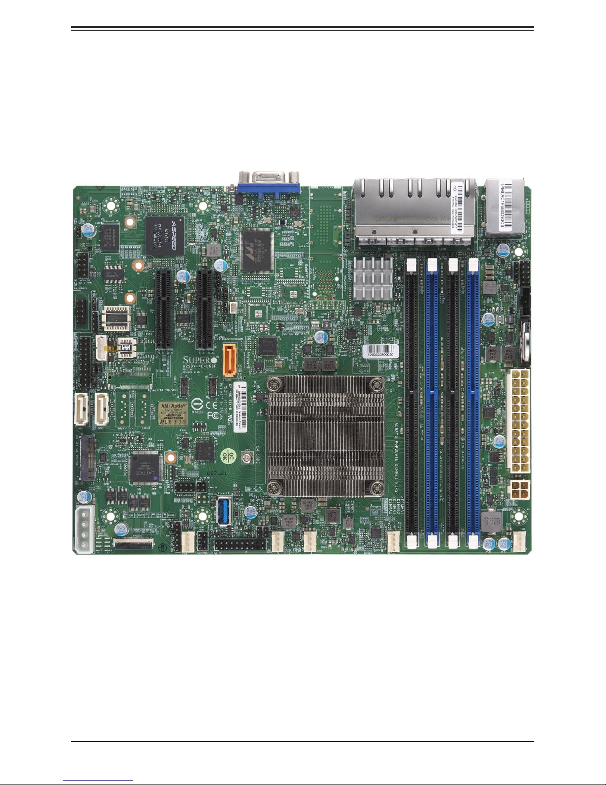
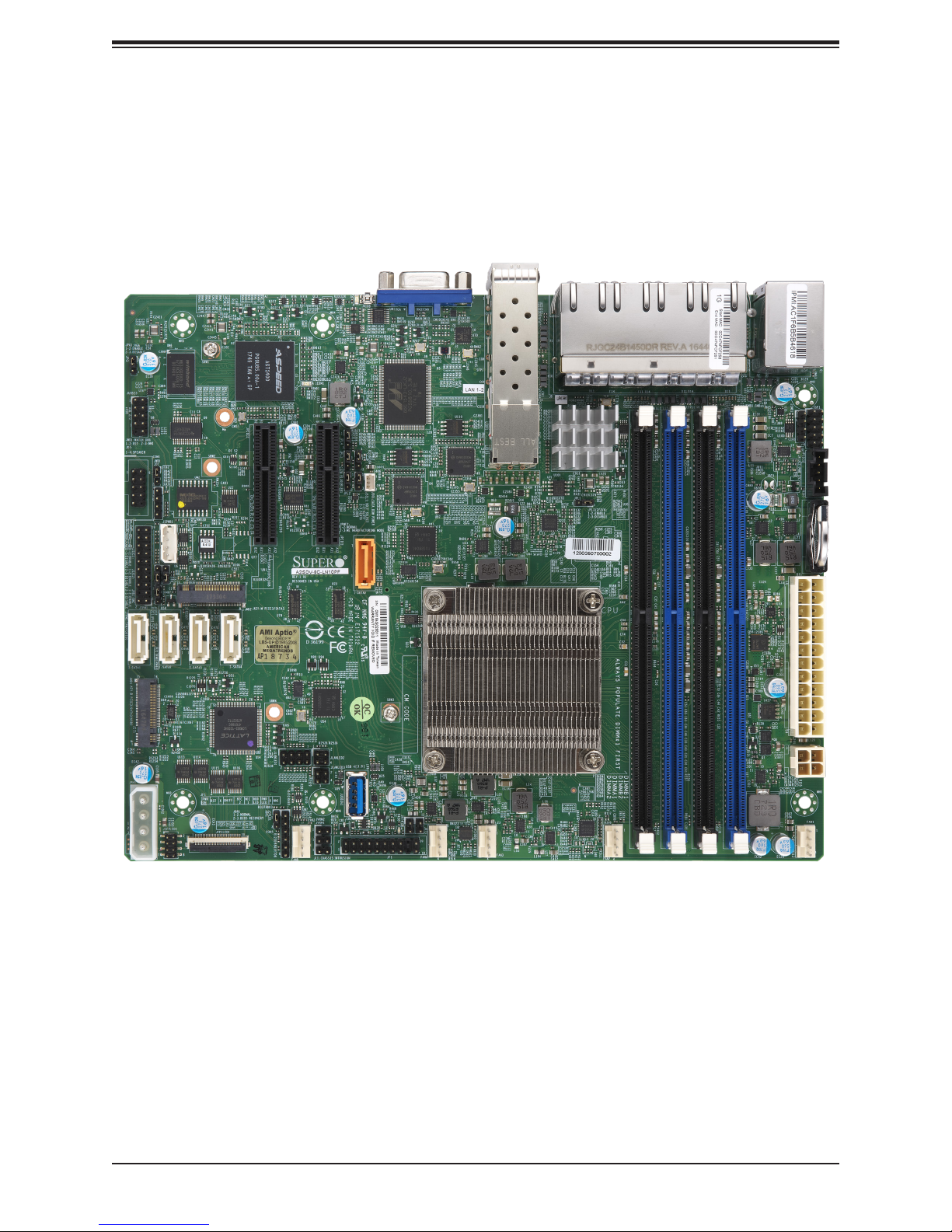
Figure 1-1. A2SDV-4C-LN8F Motherboard Image
Chapter 1: Introduction
9
A2SDV-4C/8C-LN8F/LN10PF User's Manual
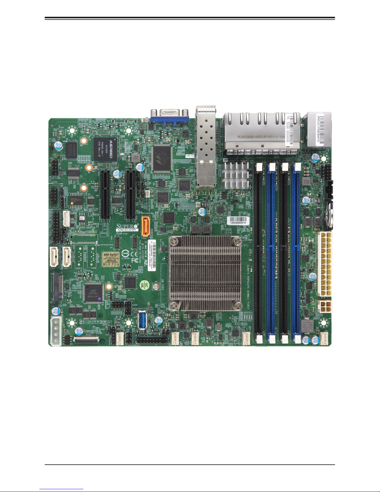
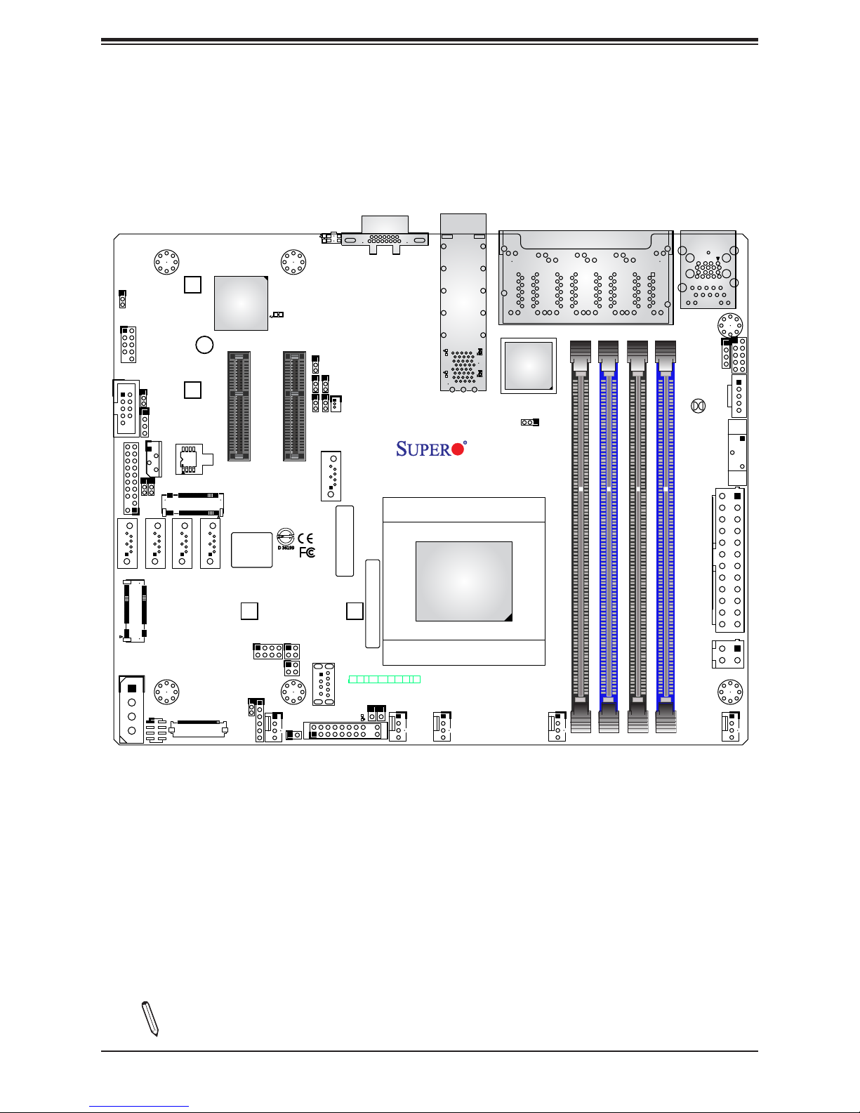
Figure 1-2. A2SDV-4C-LN10PF Motherboard Image
10
Chapter 1: Introduction
Figure 1-3. A2SDV-8C-LN10F Motherboard Image
11
A2SDV-4C/8C-LN8F/LN10PF User's Manual
JPG1
1
COM1
1
5
20
JTPM1
2
2
eUSB
JI2C1
1
USB 2/3
JWD1
JD1
JIPMB1
JI2C2
67
57
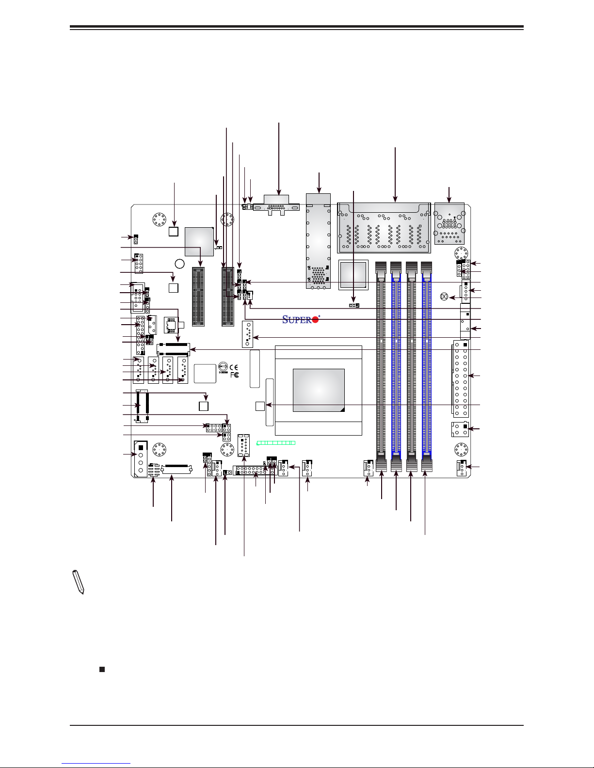
Figure 1-4. A2SDV-LN8F/LN10PF Motherboard Layout
SRW1
BMC
AST2400
M*
CPU SLOT6 PCI-E 3.0 X4
SRW2
JMD2
LEDM1
C
CPU SLOT7 PCI-E 3.0 X4
BIOS LICENSE
(not drawn to scale)
JUIDB
6
11
10
1
A
UIDLED1
VGA
A
JPL4
JPME2
JPL3
JPL2
JSD1
JSEL1
I-SATA0
BAR CODE
A2SDV-4C-LN8F
REV:1.01
DESIGNED IN USA
PRESS FIT
CG5
CG6
CG4
CG7
CG3
CG2
LEDT1 LEDT3
C
A
L20
L19
L1
C
A
CG13
CG11
SFP1
LN10PF: LAN1-2
C
A
C
A
CG1
LEDT2
LEDT4
LN10PF: LAN3-10 LN8F: LAN1-8
JPL1
ALWAYS POPULATE DIMMx1 FIRST
IPMI LAN
USB 0/1
(3.1 Gen 1)
JSMB1
JBT1
13
JPW1
JGP1
JPI2C1
BT1
1
I-SATA1
1
JPH1
I-SATA2
7475
JMD1
JSFPLED1
I-SATA3
2
1
I-SATA4
JFPCLED1
SRW4
JLANLED1
JLANLED3
JBR1
FANB
JLANLED2
2
4
USB 4 (3.1 Gen 1)
1
4
2
JL1
1
JF1
SRW3
JF1
PWR
ON
RST X
LED1
CM CODE
NIC2NIC
OH/FF
JRT3
JRT4
1
CPU
12
3
JPV1
2
DIMMA2
DIMMB2
DIMMB1
PWR
HDD
NMIX
LED
LED
1
1
20
19
FANA
FAN3
DIMMA1
FAN2
4
FAN1
Note: Components not documented are for internal testing only.
12
Quick Reference
Chapter 1: Introduction
JPG1
SLOT6
USB2/3 eUSB
SRW2
COM1
JD1
JWD1
JMD2
JIPMB1
JTPM1
JI2C1
JI2C2
I-SATA1
I-SATA2
I-SATA3
I-SATA4
SRW4
JMD1
JLANLED2
JLANLED1
JLANLED3
JPH1
Notes:
JPG1
eUSB
USB 2/3
2
1
COM1
1
JWD1
JD1
5
JIPMB1
20
JTPM1
JI2C1
JI2C2
1
2
I-SATA2
I-SATA1
7475
JMD1
1
JPH1
JSFPLED1
JSFPLED1
JFPCLED1
SRW1
SRW1
SRW2
67
57
I-SATA3
JFPCLED1
1
2
JMD2
SLOT7
LEDM1
BMC
AST2400
M*
CPU SLOT6 PCI-E 3.0 X4
BIOS LICENSE
I-SATA4
SRW4
JLANLED1
JLANLED3
JBR1
JBR1
FANB
JPL2
JPL3
JPL4
UIDLED1
JUIDB
A
JUIDB
UIDLED1
LEDM1
C
A
JPL4
CPU SLOT7 PCI-E 3.0 X4
FANB
JPL3
JPL2
JLANLED2
2
4
USB 4 (3.1 Gen 1)
4
2
JL1
1
1
JPME2
JSEL1
JSD1
JF1
JF1
JL1
USB4 (3.1 Gen 1)
6
I-SATA0
BAR CODE
SRW3
JF1
PWR
ON
VGA
11
10
1
VGA
A2SDV-4C-LN8F
REV:1.01
DESIGNED IN USA
CM CODE
HDD
NIC2NIC
OH/FF
RST X
LED
1
JRT3
JRT4
LED1
1
1
20
19
JRT3
JRT4
LED1
PWR
LED
SFP1
LN10PF: LAN1-2
PRESS FIT
CG5
CG6
CG4
CG7
CG3
CG2
CG1
LEDT1 LEDT3
NMIX
FANA
LEDT2
C
C
A
A
L20
L19
L1
C
LEDT4
C
A
A
CG13
CG11
SFP1
LN10PF: LAN1-2
CPU
FAN3
FAN3
FANA
LN10PF: LAN3-10
LN8F: LAN1-8
JPL1
LN10PF: LAN3-10 LN8F: LAN1-8
JPL1
ALWAYS POPULATE DIMMx1 FIRST
DIMMA2
DIMMB2
DIMMB1
DIMMA1
FAN2
FAN2
DIMMA2
DIMMA1
DIMMB2
DIMMB1
IPMI LAN
USB0/1 (3.1 Gen 1)
IPMI LAN
USB 0/1
(3.1 Gen 1)
JSMB1
JGP1
JBT1
JPI2C1
JGP1
JSMB1
JPME2
JPI2C1
JBT1
JSD1
JSEL1
BT1
BT1
1
I-SATA0
13
JMD2
JPW1
JPV1
FAN1
3
4
JPW1
SRW3
12
JPV1
2
FAN1
• USB 3.1 Gen 1 is also referred to as USB 3.0.
• See Chapter 2 for detailed information on jumpers, I/O ports, and JF1 front panel connec-
tions. Jumpers/LED indicators not indicated are used for testing only.
• " " indicates the location of Pin 1.
• When JLED1 (Onboard Power LED indicator) is on, system power is on. Unplug the power
cable before installing or removing any components.
to
13
A2SDV-4C/8C-LN8F/LN10PF User's Manual
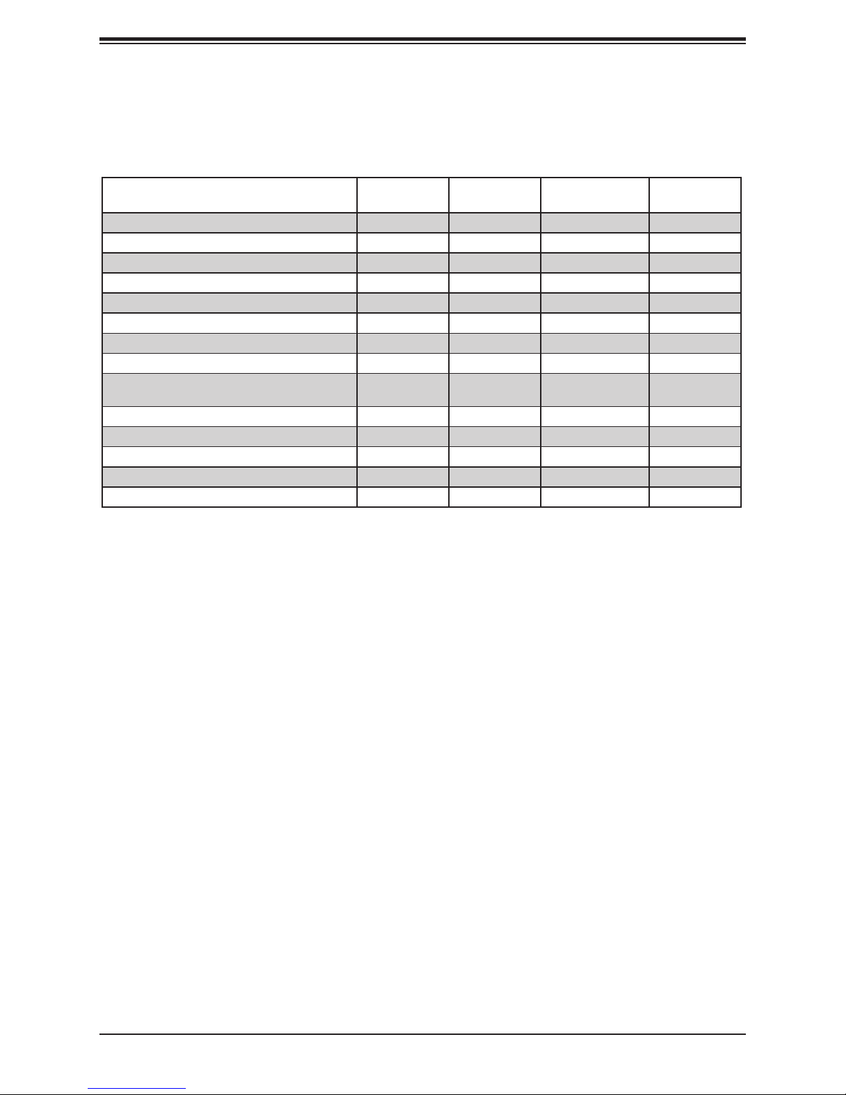
Figure 1-5. A2SDV-4C/8C-LN8F/LN10PF Model Variation Table
Motherboard Model Name A2SDV-4C-
LN8F
Processor Name C3558 C3758 C3558 C3758
Number of Cores 4 8 4 8
Number of Threads 4 8 4 8
Cache 8MB 16MB 8MB 16MB
Processor Base Frequency 2.2GHz 2.2GHz 2.2GHz 2.2GHz
Intel® Turbo Boost Frequency 2.2GHz 2.2GHz 2.2GHz 2.2GHz
SoC TDP 16W 25W 16W 25W
SATA3 Ports 3 5 1~3 5
Expansion (Slot6 or Slot7) PCI-E 3.0 x2 PCI-E 3.0 x4 PCI-E 3.0 x2
M.2 M Key No Yes No Yes
M.2 B Key Yes Yes Yes Yes
Quad GbE LAN from SoC Yes Yes Yes Yes
Quad GbE LAN from I350 Controller Ye s Ye s Yes Yes
Dual 1GbE SFP LAN from i210 Controller No No Yes Yes
A2SDV-8C-
LN8F
A2SDV-4C-LN-
10PF
or Disabled
A2SDV-8C-
LN10PF
PCI-E 3.0 x4
14

Chapter 1: Introduction
Quick Reference Table
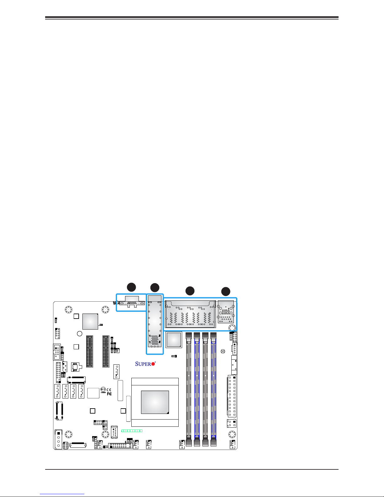
Jumper Description Default Setting
JBR1 BIOS Recovery Pins 1-2 (Normal)
JBT1 CMOS Clear Open (Normal)
JI2C1, JI2C2 SMB to PCI-E Slots Enable/Disable Pins 2-3 (Disabled)
JPG1 Onboard VGA Enable/Disable Pins 1-2 (Enabled)
JPL1 LAN1 SFP Port Enable/Disable (LN10PF only) Pins 1-2 (Enabled)
JPL2 LAN2 SFP Port Enable/Disable (LN10PF only) Pins 1-2 (Enabled)
JPL3 LN8F: LAN1-4 Ports Enable/Disable
LN10PF: LAN3-6 Ports Enable/Disable
JPL4 LN8F: LAN5-8 Ports Enable/Disable
LN10PF: LAN7-10 Ports Enable/Disable
JPME2 ME Manufacturing Mode Pins 1-2 (Normal)
JSEL1 PCI-E Slot 6/7 Selection Pins 1-2: Slot 7
JWD1 Watch Dog Timer Pins 1-2 (Reset)
Pins 1-2 (Enabled)
Pins 1-2 (Enabled)
LED Description Status
LED1 Power LED Solid Green: Power On
LEDM1 BMC Heartbeat Blinking Green: BMC Normal
UIDLED1 UID LED Solid Blue: Unit Identied
Connector Description
BT1 Onboard Battery
COM1 COM Header
FAN1 - FAN3, FANA, FANB CPU/System Fan Headers
IPMI LAN IPMI LAN Port
I-SATA0-4 SATA 3.0 Ports (SATA3/4 on -8C-LN8F/LN10PF SKUs Only)
(-4C-LN10PF: SATA1/2 are disabled when SLOT6/SLOT7 set to PCI-E 3.0 x2 in the
BIOS.)
JD1 Speaker (Pins 1-4)
JF1 Front Control Panel Header
JFPCLED1 RJ45 LAN LED Board Cable Connector for FPB-FPE300-LED10
JGP1 General Purpose I/O Header
JIPMB1 System Management Bus Header (for IPMI card)
JL1 Chassis Intrusion Header
JLANLED1 LAN3-6 Activity LED
JLANLED2 LAN7-8 Activity LED
JLANLED3 LAN9-10 Activity LED (-LN10PF SKUs Only)
JMD1 M.2 B-Key PCI-E3.0/SATA3.0/USB3.0 Slot
Note: Table is continued on the next page.
15

A2SDV-4C/8C-LN8F/LN10PF User's Manual
Connector Description
JMD2 M.2 M-Key PCI-E3.0/SATA3 Slot (8C-LN8F/LN10PF SKUs Only)
JPI2C1 Power Supply SMBus I2C Header
JPH1 4-pin Power Connector for HDD use
JPW1 24-pin ATX Power Connector
JPV1 4-pin 12V DC Power Connector (To provide alternative power for a special enclosure when
JRT3 Thermal Diode 1
JRT4 Thermal Diode 2
JSD1 SATA DOM Power Connector
JSFPLED1 SFP LAN LED Board Cable Connector for FPB-FPE300-LED10
JSMB1 System Management Bus Header
JTPM1 Trusted Platform Module (TPM)
JUIDB Unit ID Button
LAN1 - LAN10 LN8F: LAN1-8 Gigabit Ethernet RJ45 Port
SLOT6, SLOT7 Single PCI-E Expansion Slot (Slot6 or Slot7 selectable with JSEL1)
SRW1 - SRW4 M.2 Holding Screws
USB0/1 Back Panel USB 3.1 Gen 1 Ports
USB2/3 Front Accessible USB 2.0 Header
USB4 USB 3.1 Gen 1 Type A Header
VGA VGA Port
the 24-pin ATX power is not in use.)
(-LN10PF SKUs Only)
LN10PF: LAN1-2 Gigabit Ethernet SFP Port, LAN3-10 Gigabit Ethernet RJ45 Port
(8C-LN8F/LN10PF: PCI-E 3.0 x4)
(4C-LN8F: PCE-E 3.0 x2)
(4C-LN10PF: PCI-E 3.0 x2 or Disabled - Selectable in BIOS Setup)
16
Chapter 1: Introduction
Motherboard Features
Motherboard Features
CPU
• Intel® Atom SoC C3000 Series (FCBGA1310) Processor
Memory
• Supports up to 256GB of RDIMM or 64GB of Non-ECC/ECC UDIMM DDR4 memory in four slots. On select SKUs,
2400MHz modules can be used but will operate at a lower speed.
DIMM Size
• 4GB, 8GB, 16GB, and 32GB
Expansion Slots
• Two (2) PCI-E 3.0 x4 slots option (SLOT6 or SLOT 7 only) (-4C SKUs only supports PCI-E 3.0 x2)
• One (1) M.2 PCI-E 3.0/ SATA 3.0 slot (M-Key 2242/2280) (-8C-LN8F/LN10PF only)
• One (1) M.2 PCI-E 3.0/ SATA 3.0/ USB 3.0 slot (B-Key 3042/2280)
Network
• Quad RJ45 LAN with Intel C3000 SoC
• Quad RJ45 LAN with Intel i350-AM4
• Dual SFP LAN with Intel i210-IS (-LN10PF SKUs only)
Baseboard Management Controller (BMC)
• ASpeed AST2400 Baseboard Controller
Graphics
• VGA Graphics via ASpeed AST2400
I/O Devices
• Serial (COM) Header • One (1) serial header (COM1)
• 8C-LN8F/LN10PF: Five (5) SATA 3.0 ports
• SATA 3.0
• 4C-LN8F: Three (3) SATA 3.0 ports
• 4C-LN10PF: One (1) or Three (3) SATA 3.0 ports, selectable in BIOS setup
Peripheral Devices
• Three (3) USB 3.1 Gen 1 ports: two Type-A on I/O back panel (USB0/1) and one Type-A (USB4)
• Two (2) USB 2.0 ports: one internal header (USB2/3)
*USB 3.1 Gen 1 is also referred to as USB 3.0
BIOS
• 128Mb AMI BIOS® SPI Flash BIOS
• Plug and Play (PnP), SPI dual/quad speed support, rise card auto detection support, ACPI 6.1, SMBIOS 3.0, PCI FW
3.2, UEFI 2.6
Note: The table above is continued on the next page.
17
A2SDV-4C/8C-LN8F/LN10PF User's Manual
Motherboard Features
Power Management
• ACPI power management
• CPU fan auto-off in sleep mode
• Power button override mechanism
• Power-on mode for AC power recovery
System Health Monitoring
• Onboard voltage monitors for CPU cores, +3.3V, +5V, +12V, +3.3V Stby, +5V Stby, VBAT, HT, Memory, system temperature,
and memory temperature
• Status monitor for on/off control
• CPU switching phase voltage regulator
• CPU thermal trip support
Fan Control
• Five 4-pin proprietary fan headers
• Fan status monitoring via IPMI connections
• Dual cooling zone
System Management
• PECI (Platform Environment Control Interface) 3.2 support
• IPMI 2.0
• System resource alert via SuperDoctor® 5, Watch Dog, NMI
• Chassis Intrusion header and detection
• Power supply monitoring
LED Indicators
• CPU system overheat
• Power / suspend-state indicator LED
• Fan fail LED
• UID / Remote UID
• HDD activity LED
• LAN activity LED
Other
• RoHS
Dimensions
• FlexATX form factor (9" x 7.25") (228.6 mm x 184.15 mm)
Note 1: The CPU maximum thermal design power (TDP) is subject to chassis and
heatsink cooling restrictions. For proper thermal management, please check the chas-
sis and heatsink specications for proper CPU TDP sizing.
Note 2: For IPMI conguration instructions, please refer to the Embedded IPMI Conguration User's Guide available at http://www.supermicro.com/support/manuals/.
18
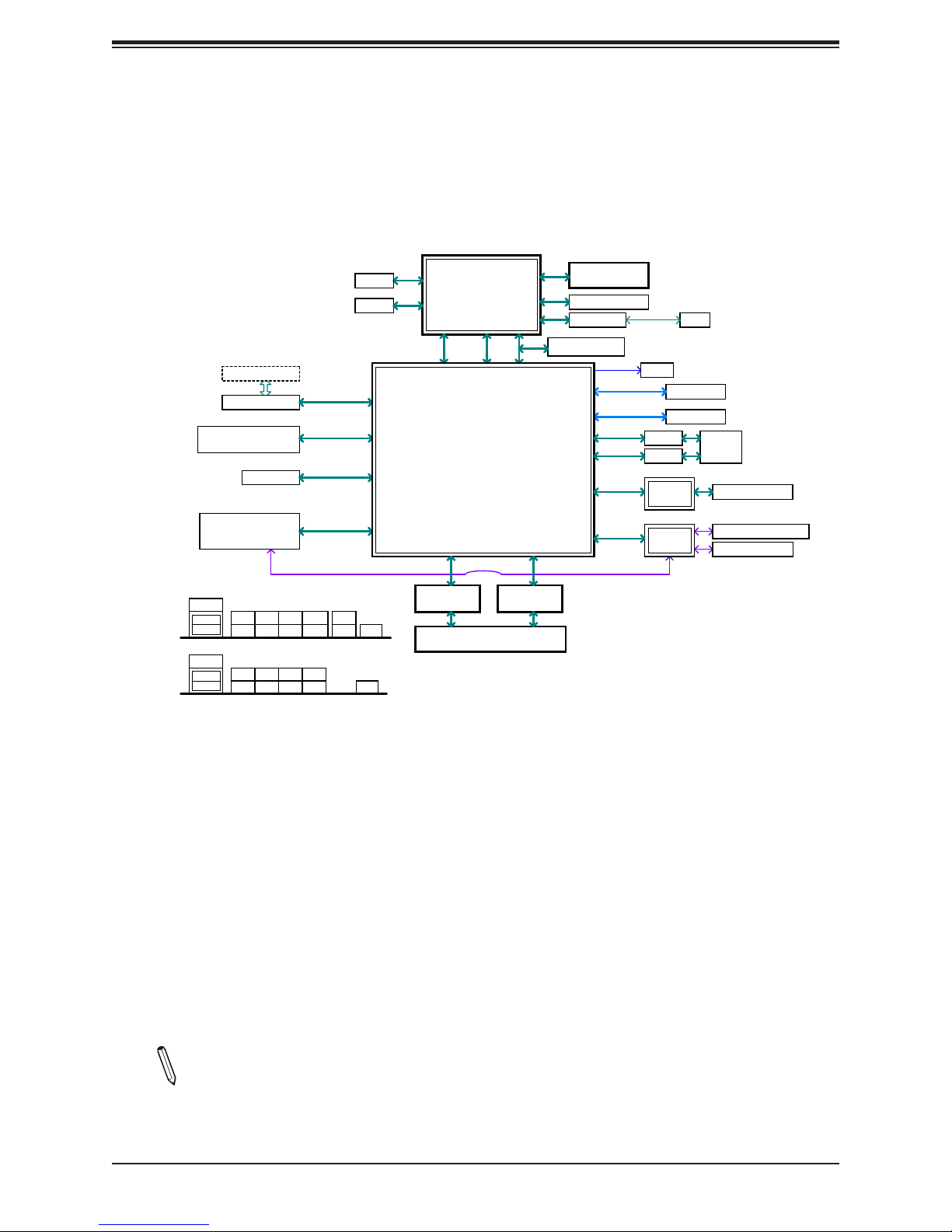
Figure 1-6.
Chipset Block Diagram
Chapter 1: Introduction
-8C-LN8F/LN10PF
SKUs only
LN10PF
LN8F
-4C SKUs: PCIE x2
PCIE X4 SLOT 6
PCIE X4 SLOT 7
M.2 2242/2280 M KEY
PCIE/SATA SSD
5X SATA-III
-4C SKUs: 3x SATA-III
M.2 3042/2280 B KEY
PCIE/SATA SSD
USB 3.0/2.0
D-LAN
USB3.0
USB3.0
D-LAN
USB3.0
USB3.0
RJ45 X 8 SFPX2
LAN4 LAN6
RJ45 X 8
LAN2
LAN4
LAN3 LAN5
LAN1
(OPTION)
PCIe 3.0_x4
8GT/s
PCIe 3.0_x2 (8GT/s)
SATA 3.0 x1 (6GT/s)
SATA-III
PCIe 3.0_x2 (8GT/s)
SATA 3.0 x1 (6GT/s)
USB 3.0 x1 / USB 2.0 x1
LAN8
LAN10
LAN7
LAN9
LAN6
LAN8
LAN7
6Gb/s
LAN2
LAN1LAN3 LAN5
VGA
FAN X5
HSIO[3:0] , PCIE x4
HSIO[5:4] , PCIE x2
HSIO[9/11/15/16/17]
SATA III
HSIO[7:6] , PCIE x2
VGA
VGA
RGB
BMC
AST2400
TACHOMETER
FCBGA1310
C3000 Series
HSIO[12:11] , PCIE x2
INTEL
I350
USB 2.0 [0]
Intel
RJ45 X 8
SMBUS2
UART1
RGMII2
LPCHSIO[14] , PCIE X1
HSIO[8] , PCIE X1
HSIO[10] , PCIE X1
HSIO[18] , USB 3.0
USB2.0[2]
HSIO[19] , USB 3.0
USB2.0[3]
KR X4
MARVELL
88E1543
CPLD
LCMXO2-1200HC
COM1 HEADER
RTL8211F
TPM Header
USB 3.0 x1
USB 2.0 x1
USB 3.0 x1
USB 2.0 x1
SVID
DDR4 (CHA)
2400MHz
DDR4 (CHB)
2400MHz
PCIE 3.0 X1
*2.5 GT/s)
PCIE 3.0 X1
*2.5 GT/s)
GIGALAN
VR13
I210IS
I210IS
USB3.0
HUB1
USB3.0
HUB2
RJ45
DIMMA1,A2
DIMMB1,B2
SFP X2
-LN10PF SKUs only
REAR USB3.0 X2
HEADER USB2.0 X2
TYPE-A USB3.0
Note 1: This is a general block diagram and may not exactly represent the features
on your motherboard. See the previous pages for the actual specications of your
motherboard.
Note 2: USB 3.1 Gen 1 is also referred to as USB 3.0.
19

A2SDV-4C/8C-LN8F/LN10PF User's Manual
1.2 Processor Overview
The Intel Atom C3000 series processor, with up to 8 cores at a 25W TDP on the A2SDV-LN8F/
LN10PF series, offers performance, reliability, and high intelligence. As a low-power systemon-a-chip motherboard, the A2SDV-4C/8C-LN8F/LN10PF is optimized for a wide variety of
networking workloads and applications.
• ACPI Power Management Logic Support Rev. 6.1
• Intel QuickAssist Technology
• Adaptive Thermal Management/Monitoring
• PCI-E 3.0, SATA 3.0 and M.2 (B-Key and M-Key) slots
• System Management Bus (SMBus) Specication Version 3.0
• Intel VT-x with Extended Page Tables (EPT)
• Intel Virtualization Technology (VT-x)
• Intel Virtualization Technology for Directed I/O (Intel VT-d)
• Intel Trusted Execution Technology (Intel TXT)
• Intel Rapid Storage Technology
• GbE Ethernet with RJ45 and SFP connectors
1.3 Special Features
This section describes the health monitoring features of the A2SDV-4C/8C-LN8F/LN10PF
motherboard. The motherboard has an onboard System Hardware Monitor chip that supports
system health monitoring.
Recovery from AC Power Loss
The Basic I/O System (BIOS) provides a setting that determines how the system will respond
when AC power is lost and then restored to the system. You can choose for the system to
remain powered off (in which case you must press the power switch to turn it back on), or
for it to automatically return to the power-on state. See the Advanced BIOS Setup section
for this setting. The default setting is Last State.
20
Chapter 1: Introduction
1.4 System Health Monitoring
This section describes the health monitoring features of the A2SDV-4C/8C-LN8F/LN10PF
motherboard. The motherboard has an onboard Baseboard Management Controller (BMC)
chip that supports system health monitoring. Once a voltage becomes unstable, a warning
is given or an error message is sent to the screen.
Onboard Voltage Monitors
The onboard voltage monitor will continuously scan crucial voltage levels. Once a voltage
becomes unstable, it will give a warning or send an error message to the screen. Users can
adjust the voltage thresholds to dene the sensitivity of the voltage monitor. Real time readings
of these voltage levels are all displayed in BIOS.
Fan Status Monitor with Firmware Control
The system health monitor embedded in the BMC chip can check the RPM status of the
cooling fans. The CPU and chassis fans are controlled via lPMI. Refer to the below table for
available fan modes to choose the most appropriate one for nominal operation.
Environmental Temperature Control
System Health sensors monitor temperatures and voltage settings of onboard processors
and the system in real time via the IPMI interface. Whenever the temperature of the CPU or
the system exceeds a user-dened threshold, system/CPU cooling fans will be turned on to
prevent the CPU or the system from overheating
Note: To avoid possible system overheating, please provide adequate airow to your
system.
System Resource Alert
This feature is available when used with SuperDoctor 5® in the Windows OS or in the Linux
environment. SuperDoctor is used to notify the user of certain system events. For example,
you can congure SuperDoctor to provide you with warnings when the system temperature,
CPU temperatures, voltages and fan speeds go beyond a predened range.
Fan Mode Description
Full Speed Use this mode to set fan speed at full speed for maximum system cooling
Standard Use this mode to set fan speed for normal system cooling
Heavy I/O Use this mode to set fan speed for higher PCI-E add-on card area cooling
Optimal Use this mode to set fan speed for normal PCI-E add-on card area cooling
PUE2 Use this mode to set fan speed for best power effi ciency and maximum noise reduction
Figure 1-7. Fan Speed Modes
21

A2SDV-4C/8C-LN8F/LN10PF User's Manual
1.5 ACPI Features
ACPI stands for Advanced Conguration and Power Interface. The ACPI specication denes
a exible and abstract hardware interface that provides a standard way to integrate power
management features throughout a computer system, including its hardware, operating
system and application software. This enables the system to automatically turn on and off
peripherals such as CD-ROMs, network cards, hard disk drives and printers.
In addition to enabling operating system-directed power management, ACPI also provides a
generic system event mechanism for Plug and Play, and an operating system-independent
interface for conguration control. ACPI leverages the Plug and Play BIOS data structures,
while providing a processor architecture-independent implementation that is compatible with
Windows® 2012.
1.6 Power Supply
As with all computer products, a stable power source is necessary for proper and reliable
operation. It is even more important for processors that have high CPU clock rates.In areas
where noisy power transmission is present, you may choose to install a line lter to shield
the computer from noise. It is recommended that you also install a power surge protector to
help avoid problems caused by power surges.
1.7 Super I/O
The Super I/O (Aspeed AST2400 chip) includes a data separator, write pre-compensation
circuitry, decode logic, data rate selection, a clock generator, drive interface control logic and
interrupt and DMA logic. The wide range of functions integrated onto the Super I/O greatly
reduces the number of components required for interfacing with oppy disk drives.
The Super I/O provides one high-speed, 16550 compatible serial communication port
(UART), which supports serial infrared communication. The UART includes a 16-byte send/
receive FIFO, a programmable baud rate generator, complete modem control capability
and a processor interrupt system. The UART provides legacy speed with baud rate of up to
115.2 Kbps as well as an advanced speed with baud rates of 250 K, 500 K, or 1 Mb/s, which
supports higher speed modems.
The Super I/O provides functions that comply with ACPI (Advanced Conguration and Power
Interface), which includes support of legacy and ACPI power management through a SMI
or SCI function pin. It also features auto power management to reduce power consumption.
The IRQs, DMAs and I/O space resources of the Super I/O can be exibly adjusted to meet
ISA PnP requirements, which support ACPI and APM (Advanced Power Management).
22

Chapter 2: Installation
Chapter 2
Installation
2.1 Static-Sensitive Devices
Electrostatic Discharge (ESD) can damage electronic com ponents. To prevent damage to your
motherboard, it is important to handle it very carefully. The following measures are generally
sufcient to protect your equipment from ESD.
Precautions
• Use a grounded wrist strap designed to prevent static discharge.
• Touch a grounded metal object before removing the board from the antistatic bag.
• Handle the board by its edges only; do not touch its components, peripheral chips, memory
modules or gold contacts.
• When handling chips or modules, avoid touching their pins.
• Put the motherboard and peripherals back into their antistatic bags when not in use.
• For grounding purposes, make sure your computer chassis provides excellent conductivity
between the power supply, the case, the mounting fasteners and the motherboard.
• Use only the correct type of onboard CMOS battery. Do not install the onboard battery
upside down to avoid possible explosion.
Unpacking
The motherboard is shipped in antistatic packaging to avoid static damage. When unpacking
the motherboard, make sure that the person handling it is static protected.
23
A2SDV-4C/8C-LN8F/LN10PF User's Manual
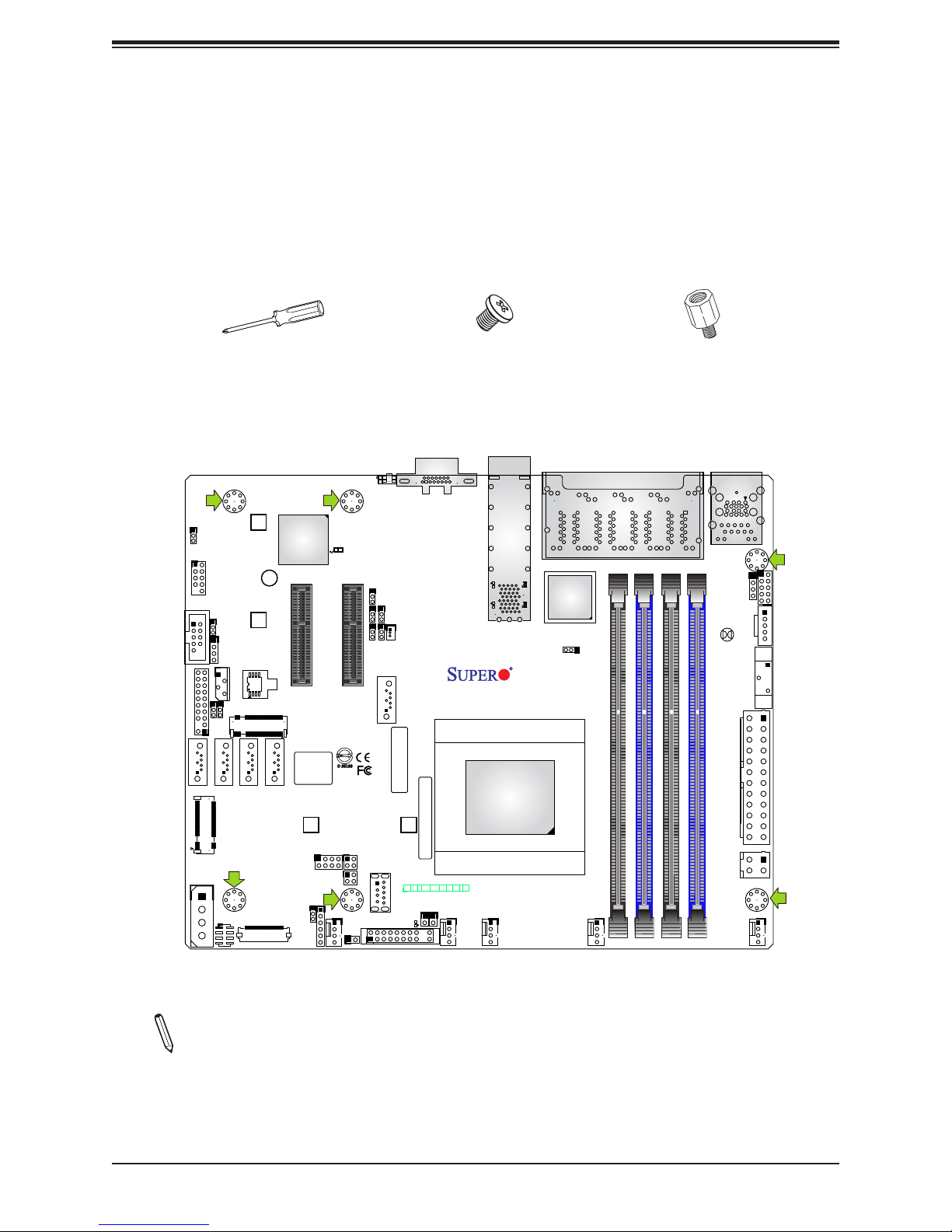
2.2 Motherboard Installation
All motherboards have standard mounting holes to t different types of chassis. Make sure
that the locations of all the mounting holes for both the motherboard and the chassis match.
Although a chassis may have both plastic and metal mounting fasteners, metal ones are
highly recommended because they ground the motherboard to the chassis. Make sure that
the metal standoffs click in or are screwed in tightly.
Phillips Screwdriver (1)
Tools Needed
JPG1
1
COM1
1
5
JTPM1
2
I-SATA1
1
JPH1
2
20
eUSB
USB 2/3
JWD1
JD1
JIPMB1
JI2C1
JI2C2
1
I-SATA2
7475
JMD1
JSFPLED1
67
I-SATA3
2
57
1
SRW1
BMC
AST2400
M*
CPU SLOT6 PCI-E 3.0 X4
SRW2
JMD2
I-SATA4
JFPCLED1
BIOS LICENSE
SRW4
JLANLED1
JLANLED3
JBR1
A
JUIDB
UIDLED1
LEDM1
C
A
JPL4
CPU SLOT7 PCI-E 3.0 X4
JPME2
JPL3
JPL2
JSD1
JSEL1
JLANLED2
2
4
USB 4 (3.1 Gen 1)
1
4
FANB
2
JL1
1
Phillips Screws (6)
11
10
1
6
I-SATA0
BAR CODE
SRW3
JF1
PWR
ON
JF1
RST X
LED1
VGA
CM CODE
OH/FF
JRT4
1
NIC2NIC
1
JRT3
1
20
19
CG6
CG7
LEDT1 LEDT3
C
A
L20
L19
L1
C
A
CG11
SFP1
LN10PF: LAN1-2
A2SDV-4C-LN8F
REV:1.01
DESIGNED IN USA
CPU
PWR
HDD
NMIX
LED
LED
FANA
FAN3
Standoffs (6)
Only if Needed
PRESS FIT
CG5
CG4
CG3
CG2
CG1
LN10PF: LAN3-10 LN8F: LAN1-8
LEDT2
C
A
LEDT4
C
A
CG13
JPL1
ALWAYS POPULATE DIMMx1 FIRST
DIMMA2
DIMMB2
DIMMB1
DIMMA1
FAN2
IPMI LAN
USB 0/1
(3.1 Gen 1)
JBT1
JPW1
JPV1
FAN1
JSMB1
JGP1
JPI2C1
BT1
13
3
4
1
12
2
Location of Mounting Holes
Note: 1) To avoid damaging the motherboard and its components, please do not use
a force greater than 8 lb/inch on each mounting screw during motherboard installation.
2) Some components are very close to the mounting holes. Please take precautionary
measures to avoid damaging these components when installing the motherboard to
the chassis.
24
Chapter 2: Installation
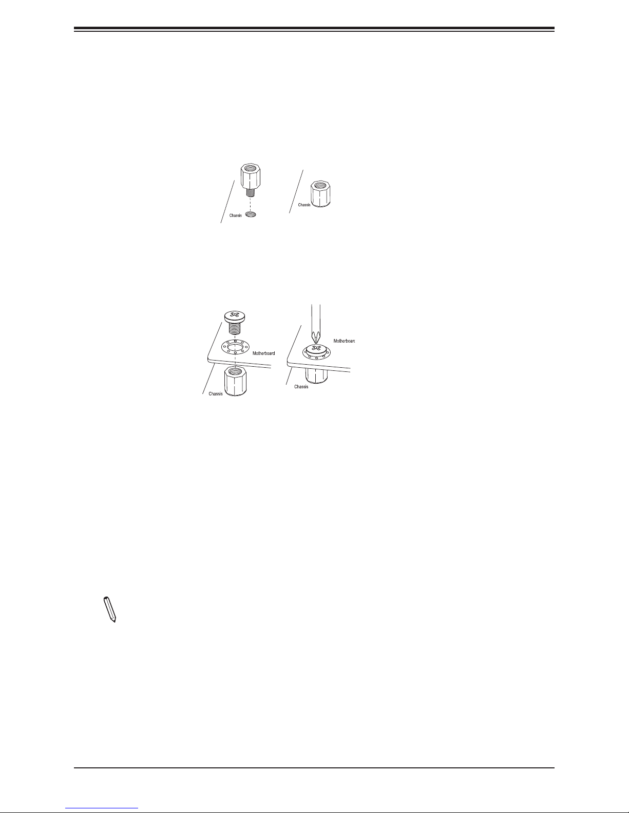
Installing the Motherboard
1. Locate the mounting holes on the motherboard. See the previous page for the location.
2. Locate the matching mounting holes on the chassis. Align the mounting holes on the
motherboard against the mounting holes on the chassis.
3. Install standoffs in the chassis as needed.
4. Install the motherboard into the chassis carefully to avoid damaging other motherboard
components.
5. Using the Phillips screwdriver, insert a Phillips head #6 screw into a mounting hole on
the motherboard and its matching mounting hole on the chassis.
6. Repeat Step 5 to insert #6 screws into all mounting holes.
7. Make sure that the motherboard is securely placed in the chassis.
Note: Images displayed are for illustration only. Your chassis or components might
look different from those shown in this manual.
25
A2SDV-4C/8C-LN8F/LN10PF User's Manual
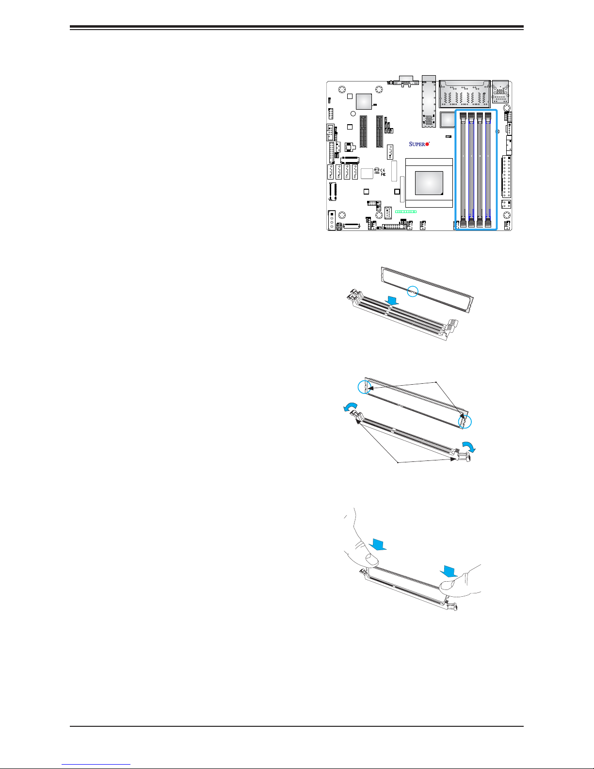
2.3 Memory Support and Installation
Note: Refer to the motherboard product page for the list of supported memory.
Important: Exercise extreme care when installing or removing DIMM modules to pre-
vent any possible damage.
Memory Support
The A2SDV-4C/8C-LN8F/LN10PF motherboard supports up to 256GB of ECC RDIMM or
64GB of Non-EC/ECC UDIMM DDR4 memory in four memory slots. Populating these DIMM
slots with memory modules of the same type and size will result in interleaved memory, which
will improve memory performance.
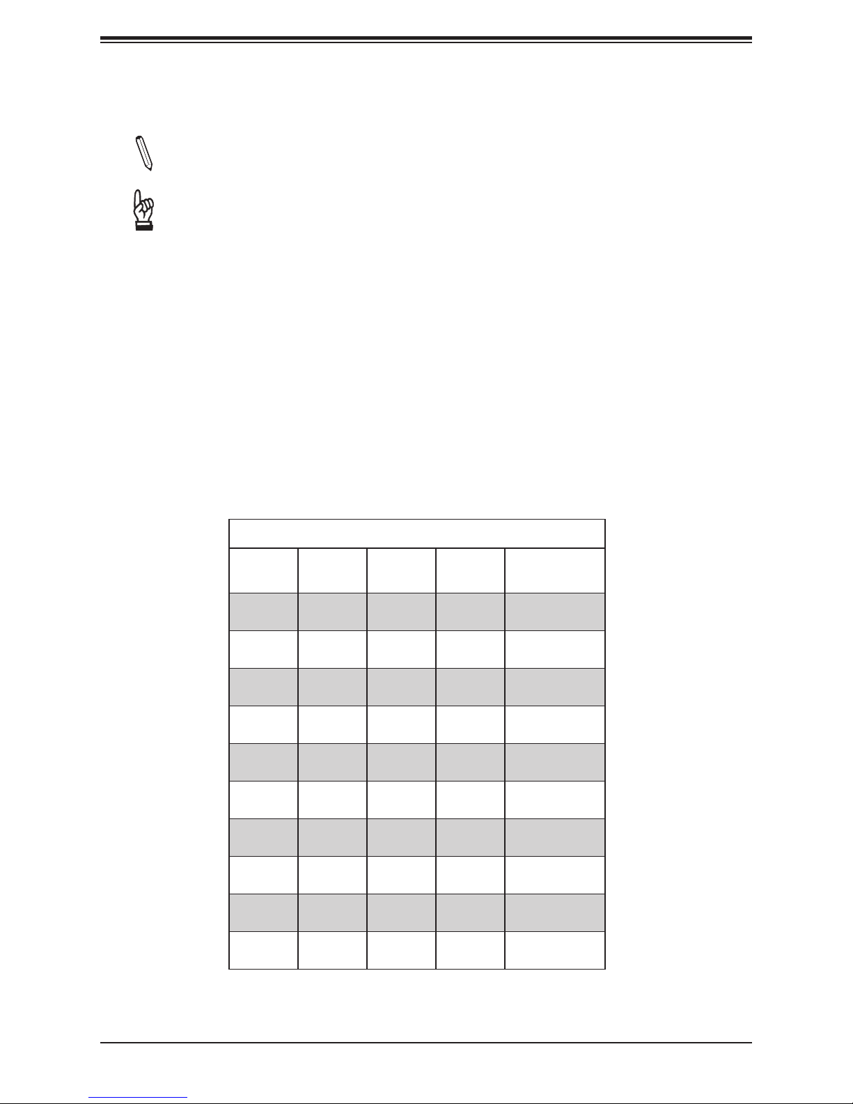
DIMM Module Population Conguration
For optimal memory performance, follow the table below when populating memory.
Memory Population (Balanced)
DIMMA1 DIMMB1 DIMMA2 DIMMB2
4GB 4GB 8GB
4GB 4GB 4GB 4GB 16GB
8GB 8GB 16GB
8GB 8GB 8GB 8GB 32GB
16GB 16GB 32GB
16GB 16GB 16GB 16GB 64GB
32GB 32GB 64GB
Total System
Memory
32GB 32GB 32GB 32GB 128GB
64GB 64GB 128GB
64GB 64GB 64GB 64GB 256GB
26
Chapter 2: Installation
DIMM Module Population Sequence
When installing memory modules, the DIMM slots should be populated in the following order:
DIMMA1, DIMMB1, DIMMA2, DIMMB2.
• Always use DDR4 DIMM modules of the same type, size and speed.
• Mixed DIMM speeds can be installed. However, all DIMMs will run at the speed of the
slowest DIMM.
• The motherboard will support odd-numbered modules (one or three modules installed).
However, for best memory performance, install DIMM modules in pairs to activate memory
interleaving.
JPG1
1
COM1
1
5
JTPM1
2
I-SATA1
1
JPH1
eUSB
2
20
1
USB 2/3
JWD1
JD1
JIPMB1
JI2C1
JI2C2
I-SATA2
7475
JMD1
JSFPLED1
67
57
I-SATA3
1
2
SRW1
SRW2
JMD2
I-SATA4
JFPCLED1
BMC
AST2400
M*
CPU SLOT6 PCI-E 3.0 X4
BIOS LICENSE
SRW4
JLANLED1
JLANLED3
JBR1
FANB
A
JUIDB
UIDLED1
6
LEDM1
C
A
JPL4
CPU SLOT7 PCI-E 3.0 X4
JPME2
JPL3
JPL2
JSD1
JSEL1
I-SATA0
BAR CODE
SRW3
JLANLED2
2
4
USB 4 (3.1 Gen 1)
JF1
1
PWR
ON
4
JF1
2
JL1
1
11
10
1
VGA
A2SDV-4C-LN8F
REV:1.01
DESIGNED IN USA
CM CODE
HDD
NIC2NIC
OH/FF
RST X
LED
1
JRT3
JRT4
LED1
1
1
20
19
PWR
LED
FANA
NMIX
PRESS FIT
CG6
CG7
LEDT1 LEDT3
C
A
L20
L19
L1
C
A
CG13
CG11
SFP1
LN10PF: LAN1-2
CPU
FAN3
CG5
CG4
CG3
CG2
CG1
LN10PF: LAN3-10 LN8F: LAN1-8
LEDT2
C
A
LEDT4
C
A
IPMI LAN
USB 0/1
(3.1 Gen 1)
JBT1
JSMB1
JGP1
JPI2C1
JPL1
BT1
13
1
ALWAYS POPULATE DIMMx1 FIRST
JPW1
DIMMB1
DIMMB2
DIMMA1
DIMMA2
12
3
JPV1
2
DIMMA2
FAN2
DIMMB2
DIMMB1
DIMMA1
4
FAN1
27
A2SDV-4C/8C-LN8F/LN10PF User's Manual
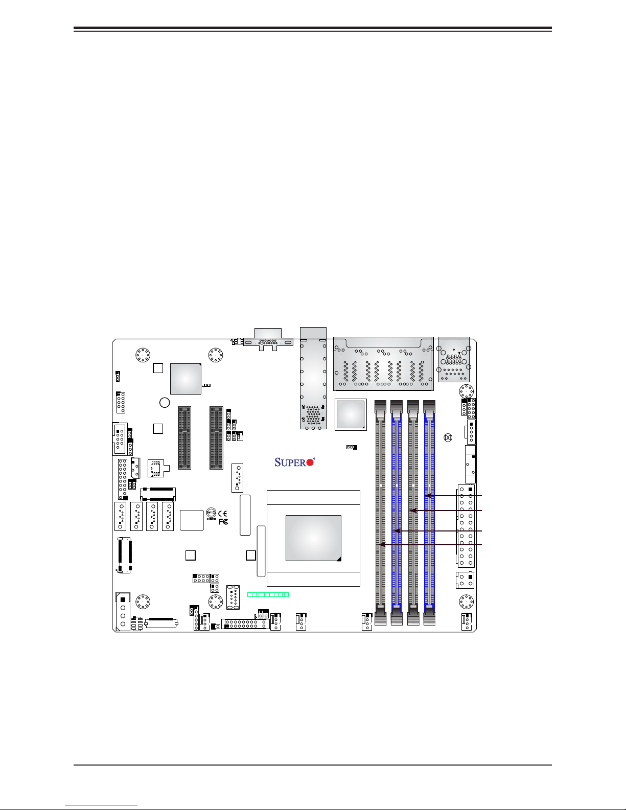
DIMM Installation
1. Insert the desired number of DIMMs into
the memory slots, starting with DIMMA1,
DIMMB1, DIMMA2, DIMMB2. For best
performance, please use the memory
modules of the same type and speed.
2. Push the release tabs outwards on both
ends of the DIMM slot to unlock it.
3. Align the key of the DIMM module with the
receptive point on the memory slot.
4. Align the notches on both ends of the
module against the receptive points on the
ends of the slot.
5. Press both ends of the module straight
down into the slot until the module snaps
into place.
10
1
VGA
A2SDV-4C-LN8F
REV:1.01
DESIGNED IN USA
PWR
HDD
NIC2NIC
NMIX
LED
LED
1
JRT3
1
20
19
FANA
CG6
CG7
LEDT1 LEDT3
C
A
L20
L19
L1
C
A
CG11
SFP1
LN10PF: LAN1-2
CPU
FAN3
PRESS FIT
CG5
CG4
CG3
CG2
CG1
LEDT2
C
A
LEDT4
C
A
CG13
LN10PF: LAN3-10 LN8F: LAN1-8
JPL1
ALWAYS POPULATE DIMMx1 FIRST
DIMMA2
DIMMB2
DIMMB1
DIMMA1
FAN2
IPMI LAN
USB 0/1
(3.1 Gen 1)
JBT1
JSMB1
JGP1
JPI2C1
BT1
13
1
JPW1
12
3
JPV1
2
4
FAN1
11
A
JUIDB
UIDLED1
6
JPG1
SRW1
BMC
AST2400
LEDM1
C
M*
CPU SLOT6 PCI-E 3.0 X4
SRW2
JMD2
I-SATA4
JFPCLED1
BIOS LICENSE
SRW4
JBR1
JLANLED1
JLANLED3
A
JPL4
CPU SLOT7 PCI-E 3.0 X4
JPL3
JPL2
JSEL1
JLANLED2
2
4
USB 4 (3.1 Gen 1)
1
4
FANB
2
JL1
1
JPME2
JSD1
I-SATA0
BAR CODE
CM CODE
SRW3
JF1
PWR
OH/FF
RST X
ON
JRT4
LED1
1
JF1
eUSB
USB 2/3
2
1
COM1
1
JWD1
JD1
5
JIPMB1
20
JTPM1
JI2C1
JI2C2
1
67
57
2
I-SATA2
I-SATA1
I-SATA3
7475
JMD1
1
JPH1
JSFPLED1
1
2
6. Press the release tabs to the lock positions
to secure the DIMM module into the slot.
DIMM Removal
Press both release tabs on the ends of the
DIMM module to unlock it. Once the DIMM
module is loosened, remove it from the
memory slot.
Notches
Release Tabs
Press both notches
straight down into
the memory slot.
28
Chapter 2: Installation
FAN3
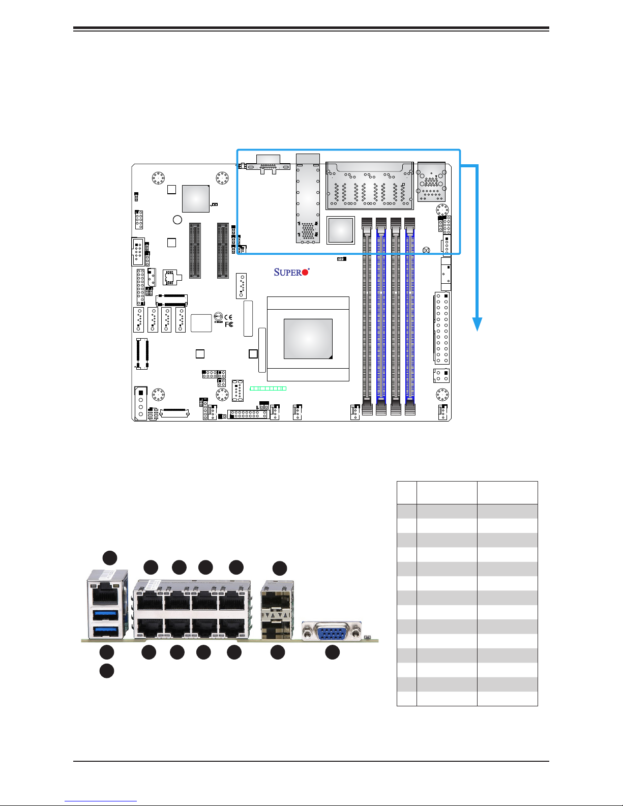
2.4 Rear I/O Ports
See Figure 2-1 below for the locations and descriptions of the various I/O ports on the rear
of the motherboard.
1
COM1
1
5
JTPM1
2
I-SATA1
1
JPH1
JPG1
2
20
eUSB
USB 2/3
JWD1
JD1
JIPMB1
JI2C1
JI2C2
1
I-SATA2
7475
JMD1
JSFPLED1
LEDT1 LEDT3
NMIX
PRESS FIT
CG5
CG6
CG4
CG7
CG3
CG2
CG1
C
C
A
A
L20
L19
L1
C
C
A
A
CG13
CG11
SFP1
LN10PF: LAN1-2
CPU
LN10PF: LAN3-10 LN8F: LAN1-8
LEDT2
LEDT4
JPL1
DIMMA2
DIMMB2
DIMMA1
FAN2
ALWAYS POPULATE DIMMx1 FIRST
DIMMB1
2
67
I-SATA3
1
SRW1
SRW2
JMD2
57
JFPCLED1
BMC
AST2400
M*
CPU SLOT6 PCI-E 3.0 X4
BIOS LICENSE
I-SATA4
SRW4
JLANLED1
JLANLED3
JBR1
A
JUIDB
UIDLED1
LEDM1
C
A
JPL4
CPU SLOT7 PCI-E 3.0 X4
JPME2
JPL3
JPL2
JSD1
JSEL1
JLANLED2
2
4
USB 4 (3.1 Gen 1)
1
4
FANB
JF1
2
JL1
1
6
I-SATA0
BAR CODE
SRW3
JF1
PWR
ON
RST X
LED1
11
10
1
VGA
A2SDV-4C-LN8F
REV:1.01
DESIGNED IN USA
CM CODE
PWR
HDD
NIC2NIC
OH/FF
LED
LED
1
JRT3
JRT4
1
1
20
19
FANA
Figure 2-1. I/O Port Locations and Denitions
IPMI LAN
USB 0/1
(3.1 Gen 1)
JBT1
JPW1
JPV1
FAN1
JSMB1
JGP1
JPI2C1
BT1
13
3
4
1
12
2
#
-LN8F
Description
-LN10PF
Description
1 IPMI LAN IPMI LAN
2 USB1 USB1
3 USB0 USB0
1
10
8
6
4
12
4 LAN2 LAN4
5 LAN1 LAN3
6 LAN4 LAN6
7 LAN3 LAN5
8 LAN6 LAN8
9 LAN5 LAN7
10 LAN8 LAN10
2
5
11
9
7
3
13
14
11 LAN7 LAN9
12 N/A LAN2
13 N/A LAN1
14 VGA VGA
29
A2SDV-4C/8C-LN8F/LN10PF User's Manual
VGA Port
A VGA port is located on the I/O back panel. Use this port to connect to a compatible VGA
display.
LAN Ports
There are eight LAN ports on the -LN8F motherboard and 10 LAN ports on the -LN10PF
motherboard. The LN10PF supports two SFP connectors on LAN1~2 and eight RJ45
connectors on LAN3~10. The LN8F supports eight RJ45 GbE LAN on LAN1~8. The
motherboard also offers one IPMI LAN port.
• LN8F SKUs: LAN1~8 (RJ45)
• LN10PF SKUs: LAN1~2 (SFP) + LAN3~10 (RJ45)
1
COM1
1
5
JTPM1
I-SATA1
1
JPH1
JPG1
20
2
eUSB
USB 2/3
2
JI2C1
1
I-SATA2
7475
JSFPLED1
JWD1
JD1
JIPMB1
JI2C2
JMD1
67
I-SATA3
2
SRW1
SRW2
57
JFPCLED1
1
JMD2
BMC
AST2400
M*
CPU SLOT6 PCI-E 3.0 X4
BIOS LICENSE
I-SATA4
SRW4
JLANLED1
JLANLED3
JBR1
A
JUIDB
UIDLED1
LEDM1
C
A
JPL4
CPU SLOT7 PCI-E 3.0 X4
JPME2
JPL3
JPL2
JSD1
JSEL1
JLANLED2
2
4
USB 4 (3.1 Gen 1)
1
4
FANB
2
JL1
1
6
I-SATA0
BAR CODE
SRW3
JF1
1
11
1
VGA
CM CODE
JF1
NIC2NIC
PWR
OH/FF
RST X
ON
JRT3
JRT4
LED1
1
1
20
19
2
10
CG6
CG7
LEDT1 LEDT3
C
A
L20
L19
L1
C
A
CG11
SFP1
LN10PF: LAN1-2
A2SDV-4C-LN8F
REV:1.01
DESIGNED IN USA
CPU
PWR
HDD
NMIX
LED
LED
1
FANA
FAN3
PRESS FIT
CG5
CG4
CG3
CG2
CG1
LEDT2
C
A
LEDT4
C
A
CG13
JPL1
3
LN10PF: LAN3-10 LN8F: LAN1-8
ALWAYS POPULATE DIMMx1 FIRST
DIMMA2
DIMMB2
DIMMB1
DIMMA1
FAN2
4
IPMI LAN
USB 0/1
(3.1 Gen 1)
JBT1
JPW1
JPV1
FAN1
JSMB1
JGP1
BT1
13
3
4
JPI2C1
1. VGA Port
2. LAN1-2 (LN10PF)
3. LAN1-8 (LN8F)
LAN3-10 (LN10PF)
4. IPMI LAN
1
12
2
30
 Loading...