

Page 1

SME5224AUPA-400
July 1999
UltraSPARC™-II CPU Module
DATASHEET
400 MHz CPU, 4.0 MB E-Cache
MODULE DESCRIPTION
The UltraSPARC™–II, 400 MHz CPU, 4.0 Mbyte module, (SME5224AUPA-400) delivers high performance
computing in a compact design. Based on the UltraSPARC™-II CPU, this module is designed using a small
form factor board with an integrated external cache. It connects to the high bandwidth Ultra™ Port Architecture UPA bus viaahigh speed sturdy connector. The UltraSPARC™–II,400 MHz CPU, 4.0 Mbyte module, can
plug into any UPA connector, saving system design costs and reducing the production time for new systems.
Heatsinks areattached to components on the module board. The module board is encased in a plastic shroud.
The purpose of this shroud is to protect the components and channel airflow. Module design is geared
towards ease of upgrade and field support.
Module Features Module Benefits
Ease of System Design
• Small form factor board with integrated external cache
and UPA interface
• JTAG boundary scan and performance instrumentation
• PCB provides a multi-power plane bypass, reducing
systemboard design requirements
Performance
• High performance UltraSPARC™ CPU at 400MHz
• Four megabytes of external cache using high speed
register-latch SRAMs
• Dedicated high bandwidth bus to processor
Glueless MP Support
Simplify System Qualifications by
Complying with Industry and Government
Standards
•
• Implements the high performance AUPA interface
• Supports up to 16 Mbyte of external cache in a
four-way MP system
• Backwards compatibility with systems implementing a
UPA interface
• Plastic shroud protects components and channels
airflow
• Multi-layer PCB controls EMI radiation
• Edge connectors and ejectors
• Small form factor board encased in a heat resistant
shroud
• On-board voltage regulator accepts 2.6 volts for the
Vdd_core; compatible with existing systems
1
Page 2

™
UltraSPARC
SME5224AUPA-400 400 MHz CPU, 4.0 MB E-Cache
-II CPU Module
CPU DESCRIPTION
UltraSPARC-II CPU
The UltraSPARC™-II CPU is the second generation in the UltraSPARC™ s-series microprocessor family.
A complete implementation of the SPARCV9 architecture, it has binary compatibility with all previous versions of the SPARC™ microprocessor family.
The UltraSPARC™-II CPU is designed as a cost effective, scalable and reliable solution for high-end workstations and servers. Meeting the demands of mission critical enterprise computing, theUltraSPARC™-II CPU
runs enterprise applications requiring high data throughput. It is characterized by a high integer and floating
point performance: optimally accelerating application performance, especially multimedia applications.
Delivering high memory bandwidth, media processing and raw compute performance, the UltraSPARC™-II
CPU incorporates innovative technologies which lower the cost of ownership.
CPU Features CPU Benefits
Architecture
•Thirty-two 64-bit integer registers • Allows applications to store data locally in the
•Superscalar/Superpipelined • Allows for multiple integer and floating point
•High performance memory interconnect • Alleviating the bottleneck of bandwidth to main
•Built-in Multiprocessing Capability • Delivering scalability at the system level, thus
•VIS multimedia accelerating instructions • Reducing the system cost by eliminating the
•100% binary compatibility with previous versions
of SPARC™
•Uses 0.25 micron technology and packaging • Enhanced processor performance with decreased
• 64-bit SPARC-V9 architecture increases the
network computing application’s performance
register files
execution units leading to higher application
performance
memory
increasing the end user’s return on investment
special purpose media processor
• Increasing the return on investment of software
applications
power consumption, thus increasing the reliability
of the microprocessor
Performance
•Integer • 17.4(SPECint95)
•Floating Point • 25.7 (SPECfp95)
•Bandwidth (BW) to main memory • 1.6 Gbyte/sec (peak) with a 100MHz UPA
Unique Features
•Block load and store instructions • Delivering high performance access to large
•JTAG Boundary Scan and Performance
Instrumentation
datasets across the network
• Enabling UltraSPARC™ based systems to offer
features such as: power management, automatic
error correction, and lower maintenance cost
2
Sun Microsystems, Inc
July 1999
Page 3

™
UltraSPARC
400 MHz CPU, 4.0 MB E-Cache
-II CPU Module
Advanced Version
SME5224AUPA-400
DATA BUFFER DESCRIPTION
UltraSPARC-II Data Buffer (UDB-II)
The UltraSPARC™-II module has two UltraSPARC-II data buffers (UDB-II) - each a 256 pin BGA device - for
a UPA Interconnect system bus width of 128 Data + 16 ECC.
There is a bidirectional flow of information between the external cache of the CPU and the 144-bit UPA interconnect. The information flow is linked through the UDB-II, it includes: cache fill requests, writeback data for
dirty displaced cache lines, copyback data for cache entries requested by the system, non-cacheable loads and
stores, and interrupt vectors going to and from the CPU.
Each UDB-II has a 64-bit interface plus eight parity bits on the CPU side, and a 64-bit interface plus eight error
correction code (ECC) bits on the system side.
The CPU side of the UDB-II is clocked with the same clock delivered to UltraSPARC-II (1/2 of the CPU pipeline frequency).
EXTERNAL CACHE DESCRIPTION
The external cache is connected to the E-cache data bus. Nine SRAM chips are used to implement the four
megabyte cache. One SRAM is used as the tag SRAM and eight are used as data SRAMs. The tag SRAM is
128K x 36, while the data SRAMs are 256K x 18. All nine SRAMs operate in synchronous register-latch mode.
The SRAM interface to the CPU runs at one-half of the frequency of the CPU pipeline. The SRAM signals
operate at 1.9V HSTL. The SRAM clock is a differential low-voltage HSTL input.
[1]
1. PECL (Positive Emitter Coupled Logic) clocks are converted on the module to the HSTL clocks, for the E-cache
interface.
July 1999
Sun Microsystems, Inc
3
Page 4
™
UltraSPARC
-II CPU Module
SME5224AUPA-400 400 MHz CPU, 4.0 MB E-Cache
MODULE COMPONENT OVERVIEW
The UltraSPARC™–II, 400 MHz CPU, 4.0 Mbyte module, (SME5224AUPA-400), (see Figure 1), consists of the
following components:
• UltraSPARC™-II CPU at 400 MHz
• UltraSPARC-II Data Buffer (UDB-II)
• 4.0 Megabyte E-cache, made up of eight (256K X 18) data SRAMs and one 128K X 36 Tag SRAM
• Clock Buffer: MC100LVE210
• DC-DC regulator (2.6V to 1.9V)
• Module Airflow Shroud
Block Diagram
The module block diagram for the UltraSPARC™–II, 400 MHz CPU, 4 Mbyte E-cache module
is illustrated in Figure 1.
1.9V
DC-DC
Regulator
2.6V
T ag SRAM ADDR [17:0] + Control
T ag SRAM D ATA [24:0]
T ag SRAM
128K x 36
Clock Buffer
Clocks
UltraSP ARC-II
CPU
SRAM
256K x 18
UDB-II UDB-II
UDB-II
Control
UP A Connector
UP A ADDR [35:0] + Control
SRAM ADDR [19:0] + Control
SRAM
256K x 18
DAT A [71:0]DAT A [143:72]
UP A_D ATA [143:0]
Figure 1. Module Block Diagram
4
Sun Microsystems, Inc
July 1999
Page 5
™
UltraSPARC
-II CPU Module
400 MHz CPU, 4.0 MB E-Cache
Advanced Version
SME5224AUPA-400
SYSTEM INTERFACE
Figure 2 shows the major components of a UPA based uniprocessor system. The system controller
UPA bus arbitrates betweenthe UltraSPARC™–II, 400 MHz CPU,4.0 Mbyte module, and the I/O bridgechip.
The figure also illustrates a slave-only UPA graphics port for Sun graphics boards
.
The module UPA system interface signals run at one-quarter of the rate of the internal CPU frequency.
UltraSP ARC-II
Module
SME5224AUPA-400
[1]
for the
UP A
Graphic
Device
Memory
SIMMs
144
UP A Address Bus 0
I/O Bridge
Chip
UP A Data Bus
UP A Data Bus
System
Controller
72
Cross Bar
Switch
Expansion Bus
UP A Address Bus 1
UP A Data Bus
72
Memory Data Bus
Figure 2. Uniprocessor System Configuration
UPA Connector Pins
The UPA edge connector provides impedance control. The pin assignments are shown with the physical module connector and are represented on page 24 and page 25.
UPA Interconnect
The UltraSPARC™–II, 400 MHz CPU, 4.0 Mbyte module, (SME5224AUPA-400), supports full master and
slave functionality with a 128-bit data bus and a 16-bit error correction code (ECC).
All signals that interface with the system are compatible with LVTTL levels. The clock inputs at the module
connector, CPU_CLK, UPA_CLK0, and UPA_CLK1, are differential low-voltage PECL compatible.
1. Only two megabytes of external cache are recognized and supported when using the
Dual Processor System Controller (DSC, Marketing Part No.STP2202ABGA).
July 1999
Sun Microsystems, Inc
5
Page 6

™
UltraSPARC
SME5224AUPA-400 400 MHz CPU, 4.0 MB E-Cache
-II CPU Module
Module ID
Module IDs are used to configure the UPA address of a module. The UPA_PORT_ID[4:3] are hardwired on
the module to “0”. UPA_PORT_ID[1:0] are brought out to the connector pins. Each module is hardwired in
the system to a fixed and unique UPA address. This feature supports systems with four or fewer processors.
For systems that need to support eight modules, UPA_SPEED[1] is connected to SYSID[2] in UDB-II to provide UPA_PORT_ID[2].
Systems which support more than eight modules must map the limited set of UPA_PORT_IDsfrom this module to the range of required UPA_PORT_IDs, by implementation-specific means in the system.
System firmware (Open Boot Prom) uses UPA_CONFIG_REG[42:39] for generating correct clocks to the CPU
module and the UPA system ASICs. These bits are hardwired on the module and are known at MCAP[3:0] at
the UltraSPARC-II pins. The 4-bit MCAP value for this module is 0111b.
Module Power
Two types of power are required for this module: VDDat 3.3V, and V
DD_CORE
at 2.6V. The V
DD_CORE
supplies the
DC-DC regulator which in turn supplies 1.9 volts to the core of the processor chip, the UDB-II external cache
interface I/O, and the SRAM I/O. A resistor located on the module sends the program value to the power
supply so it generates V
at 2.6V to the regulator.
DD_CORE
JTAG Interface
The JTAG TCK signal is distributed to UDB-II, SRAMs and the CPU. For additional information about the
JTAG interface, see "JTAG Testability," on page 22, and "JTAG (IEEE 1149.1) Timing," on page 23.
6
Sun Microsystems, Inc
July 1999
Page 7
™
UltraSPARC
-II CPU Module
400 MHz CPU, 4.0 MB E-Cache
Advanced Version
SME5224AUPA-400
SIGNAL DESCRIPTION
[1]
System Interface
Signal Type Name and Function
UPA_ADDR[35:0] I/O Packet switched transaction request bus. Maximum of three other masters and one
UPA_ADDR_VALID I/O Bidirectional radial UltraSPARC-II Bus signal between the UltraSPARC-II CPU and the
UPA_REQ_IN[2:0] I UltraSPARC-II system address bus arbitration request from up to three other
UPA_SC_REQ_IN I UltraSPARC-II system address bus arbitration request from the system. Used by the
UPA_S_REPLY[4:0] I UltraSPARC-II system reply packet, driven by system controller to the UPA port.
UPA_DATA_STALL I Driven by system controller to indicate whether there is a data stall. Active high.
UPA_P_REPLY[4:0] O UltraSPARC-II system reply packet, driven by the UltraSPARC-II to the system.
UPA_DATA[127:0] I/O UPA Interconnect data bus.
UPA_ECC[15:0] I/O ECC bits for the data bus. 8-bit ECC per 64-bits of data.
UPA_ECC_VALID I Driven by the system controller to indicate that the ECC is valid for the data on the
UPA_REQ_OUT I/O Arbitration request from this module: active high.
UPA_PORT_ID[1:0] I Module’s identification signals: active high. UPA_SPEED[1] acts as a
system controller can be connected to this bus. Includes 1-bit odd-parity protection.
Synchronous to UPA_CLK.
system. Driven by UltraSPARC-II to initiate UPA_ADDR transactions to the system.
Driven by system to initiate coherency, interrupt or slave transactions to
UltraSPARC-II CPU. Synchronous to UPA_CLK. Active high.
UltraSPARC-II bus ports, which may share the UPA_ADDR. Used by the
UltraSPARC-II for the distributed UPA_ADDR arbitration protocol. Connection to other
UltraSPARC-II bus ports is strictly dependent on the Master ID allocation.
Synchronous to UPA_CLK. Active high.
UltraSPARC-II CPU for the distributed UPA_ADDR arbitration protocol.
Synchronous to UPA_CLK. Active high.
Synchronous to UPA_CLK. Active high. UPA_S_REPLY [4] is a no-connect.
Synchronous to UPA_CLK. Active high.
UPA interconnect data bus: active high.
UPA_PORT_ID[2]
Clock Interface
Signal Type Name and Function
UPA_CLK[1:0]_POS
UPA_CLK[1:0]_NEG
CPU_CLK_POS
CPU_CLK_NEG
UPA_RATIO I This is not used.
UPA_SPEED [0] O UPA_SPEED [0] is an output tied low on the module
UPA_SPEED [1] I/O UPA_SPEED[1] is tied low with 510 ohms and high to 3.3V with 4.7k ohms. It is
UPA_SPEED [2] O UPA_SPEED [2] is tied low on the module
1. For the modular connector pin assignments (UPA pin-out assignments) see page 24 and page 25.
July 1999
I UPA Interconnect Clock: two copies are provided, one for the CPU and one for the
UDBs
I Differential Clock inputs to the clock buffer on the module
also connected to the SYSID [2] on each UDB-II.
Sun Microsystems, Inc
7
Page 8
™
UltraSPARC
-II CPU Module
SME5224AUPA-400 400 MHz CPU, 4.0 MB E-Cache
JTAG/Debug Interface
Signal Type Name and Function
TDO O IEEE 1149 test data output. A three-state signal driven only when the TAP controller is
TDI I IEEE 1149 test data input. This pin is internally pulled to logic one when not driven.
TCK I IEEE 1149 test clock input. This pin if not hooked to a clock source must always be
TMS I IEEE 1149 test mode select input. This pin is internally pulled to logic one when not
TRST_L I IEEE 1149 testreset input (active low).This pinis internally pulled to logic one whennot
in the shift-DR state.
driven to a logic 1 or a logic 0.
driven. Active high.
driven. Active low.
Initialization Interface
Signal Type Name and Function
UPA_RESET_L I Driven by the system controller for the POR (power-on) resets and the fatal system
UPA_XIR_L I Driven to signal externally initiated reset (XIR). Actually acts like a non-maskable
reset. Asserted asynchronously. Deasserted synchronous to UPA_CLK. Active low.
interrupt. Synchronous to UPA_CLK. Active low, asserted for one clock cycle.
Miscellaneous Signals
Signal Type Name and Function
TEMP_SENSE_NEG
TEMP_SENSE_POS
POWER_SET_POS
POWER_SET_NEG
POWER_OV O Connected to GND via a 1180-ohm resistor. Sets overvoltage level forprogrammable
1. The thermistor used on the module (SME5224AUPA-400) is manufactured by KOA. Operating at 47K the thermistor has KOA part
number NT32BT473J.
O Connected to a thermistor
O POWER_SET_NEG is tied to GND onthe module. POWER_SET_POS isconnected
to GND via a 1690-ohm resistor. Sets voltage of programmable supply.
supply.
[1]
adjacent to the CPU package.
8
Sun Microsystems, Inc
July 1999
Page 9
™
UltraSPARC
400 MHz CPU, 4.0 MB E-Cache
-II CPU Module
Advanced Version
SME5224AUPA-400
UPA AND CPU CLOCKS
Module Clocks
The module receives threedifferential pair low voltage PECL (LVPECL) clock signals (CPU_CLK, UPA_CLK0
and UPA_CLK1) from the systemboard and terminates them. The CPU_CLK is unique in the system, but the
UPA_CLKs are two of many UPA clock inputs in the system.
The CPU_CLK operates at 1/2 the CPU core frequency. The UPA_CLKs operate at the UPA bus frequency.
The CPU to UPA clock ratios refer to the CPUcore to UPAbus clock signal frequency. The CPU on the module
will automatically sense the clock ratio driven by the systemboard as long as the module clock timing is
satisfied.
The UltraSPARC-II CPU and UDB-II data buffers detect and support multiple CPU to UPA clock frequency
ratios. The UltraSPARC™–II, 400 MHz CPU, 4.0 Mbyte module is production tested in the 4:1 ratio (400 MHz
CPU and 100 MHz UPA). It can be qualified at other ratios in specific systemboards.
Tested CPU to UPA
UltraSPARC-II CPU Module
400 MHz, 4 Mbyte E-cache 4:1 3:1, 5:1, 6:1
System Clocks
The systemboard generates and distributes the CPU and UPA LVPECL clocks. The systemboard includes a
frequency generator, frequency divider, clock buffers, and terminators.
The buffers fan-out the LVPECL clocks to the many UPA devices: the module, cross-bar data switches, system
controller, FFB, and the system I/O bridge. The LVPECL clock trace pairs are routed source-to-destination.
Each net is terminated at the destination. Most destinations are to single devices. The PCB traces for the
LVPECL clocks are balanced to provide a high degree of synchronous UPA device operation.
Frequency Ratio
Other supported CPU to UPA Frequency Ratios
System Clock Distribution
The goal of this clock distribution is to deliver a quality clock to each system UPA device simultaneously and
with the correct clock relationships to the module clocks. For a discussion on how to layout and balance the
systemboard LVPECL clock signals and UPAbus signals, see the UPA Electrical Bus Design Note (Document
Part Number: 805-0089).
The effective length of the CPU_CLK, UPA_CLK0, and UPA_CLK1 clocks signals on the module are provided
in the UPA AC Timing Specification section of this data sheet.
The block diagram for the LVPECLclocks "Clock Signal Distribution," on page 10, illustrates a typical system
clock distribution network. Each clock line is a parallel-terminated, dual trace LVPECL clock signal for the
CPU, the UPA and the SRAM devices.
July 1999
Sun Microsystems, Inc
9
Page 10
™
UltraSPARC
-II CPU Module
SME5224AUPA-400 400 MHz CPU, 4.0 MB E-Cache
.
Module Boundary
SRAM
SRAM
SRAM
SRAM
SRAM
SRAM
SRAM
SRAM
SRAM/T A G
Parallel
Clock
Generator
Serial
Clock
Divider
UP A_CLK
Clock
Buffer
CPU_CLK
UP A_CLK0
Module
Connector
UDB-II
UDB-II
UP A_CLK1
UP A_CLK2
UP A_CLKx
Clock Buffer
UltraSPARC-II
CPU
UP A De vice
UP A De vice
Figure 3. Clock Signal Distribution
LOW VOLTAGE PECL
Two trace signals compose each clock: one positive signal and one negative signal. Each signal is 180-degrees
out of phase with the other. Signal timing is referenced to when the positive LVPECL signal transitions from
low to high at the cross-over point, when the negative signal transitions from high to low. The trace-pair are
routed side-by-side and use parallel termination, (specific routing techniques are require).
CPU CLOCK INPUT
The PLL in the CPU doubles the clock frequency presented at its clock pin. So, for a 400 MHz core CPU clock
frequency, the CPU_CLK signal is 200 MHz. Therefore, for the CPU, actions will appear to occur at both transitions of the input CPU_CLK.
CLOCK TRACE DELAYS
The LVPECL propagation time is constant for all clock signals so all balancing is based on length rather than
time. All LVPECL traces are striplines (dielectric and power planes top and bottom) with a fixed 180 ps per
inch propagation time using the FR4, PCB Dielectric.
10
Sun Microsystems, Inc
July 1999
Page 11

™
UltraSPARC
-II CPU Module
400 MHz CPU, 4.0 MB E-Cache
Advanced Version
SME5224AUPA-400
ELECTRICAL CHARACTERISTICS
Absolute Maximum Ratings
Symbol Parameter Rating Units
V
DD
V
DD_CORE
V
I
V
O
I
IK
I
OK
I
OL
T
STG
1. Operation of the device at values in excess of those listed above will result in degradation or destruction of the device. All voltages
are defined with respect to ground. Functional operation of thedevice at these or any other conditions beyondthose indicated under
“recommended operating conditions” is not implied. Exposure to absolute-maximum-rated conditions for extended periods may
affect device reliability.
2. The V
DD_CORE
SRAM I/O bus interface. The V
be lower than V
3. Unless otherwise noted, all voltages are with respect to the VSSground.
Supply voltage range for I/O 0 to 3.8 V
[2]
Supply voltage range for CPU core 0 to 3.0 V
Input voltage range
Output voltage range -0.5 to VDD + 0.5 V
Input clamp current ± 20 mA
Output clamp current ± 50 mA
Current into any output in the low state 50 mA
Storage temperature (non-operating) -40 to 90 °C
supplies voltage to the onboard DC-DC regulator. The onboard DC-DC regulator then powers the CPU core and the
for 30 ms or less, provided that the current is limited to twice thew maximum CPU rating.
DD_CORE
[1]
[3]
must be lower than VDD, except when the CPU is being re-cycled, at which time the VDDcan
DD_CORE
-0.5 to VDD + 0.5 V
Recommended Operating Conditions
Symbol Parameter Min Typ Max Units
V
DD
V
DD_CORE
V
SS
V
IH
V
IL
I
OH
I
OL
T
J
T
A
1. A current of 2.6V supplies power to the DC-DC regulator which in turn supplies 1.9V to the CPU core.
2. Maximum ambient temperatureis limited byairflow such that themaximum junction temperature does not exceed TJ. See the section
"Thermal Specifications," on page 18.
Supply voltage for I/O 3.14 3.30 3.46 V
Supply voltage for the CPU core
[1]
2.47 2.60 2.73 V
Ground – 0 – V
High-level input voltage 2.0 – VDD + 0.2 V
Low-level input voltage -0.3 – 0.8 V
High-level output current – – -4 mA
Low-level output current – – 8 mA
Operating junction temperature – – 85 °C
Operating ambient temperature – – –
[2]
°C
July 1999
Sun Microsystems, Inc
11
Page 12
™
UltraSPARC
-II CPU Module
SME5224AUPA-400 400 MHz CPU, 4.0 MB E-Cache
DC Characteristics
[1]
Symbol Parameter Conditions Min Typ Max Units
V
OH
V
IH
High-level output voltage VDD= Min, IOH = Max 2.4 – – V
High-level input voltage, PECL clocks, 2.28 – – V
High-level input voltage,
2.0 – – V
except PECL clocks
V
IL
Low-level input voltage, PECL clocks – – 1.49 V
Low-level input voltage,
– – 0.8 V
except PECL clocks
V
OL
I
DD
I
DD_CORE
I
OZ
Low-level output voltage VDD= Min, IOL = Max – – 0.4 V
Supply current for V
Supply current for V
High-impedance output current
(Outputs without pull-ups)
High-impedance output current
[2] [3]
DD
DD_CORE
[4] [3]
VDD = Max, Freq.=Max – 9.3 12.04 A
V
= Max, Freq.=Max – 10.05 11.6 A
DD_CORE
VDD= Max, VO= 0.4V to 2.4V – – 30 µA
– – -30 µA
VDD = Max, VO = VSS to V
– – 250 µA
DD
(Outputs with pull-ups)
I
I
I
OH
I
OL
1. Note that this tables specifies the DC characteristics at the UPA 128M connector.
2. The supply current for the VDDincludes the supply current for the CPU, UDB-II, and the SRAMs.
3. The typical DC current values represent the current drawn at nominal voltage with a typical, busy computing load. Variations in the
device, computing load, and system implementation affect the actual current. The maximum DC current values will rarely, if ever, be
exceeded running all known computing loads over the entire operating range. The maximum values are based on simulations.
4. The supply current for the V
Input current (inputs without pull-ups) VDD = Max, VI = VSS to V
Input current (inputs with pull-ups) VDD = Max, VI = VSS to V
DD
DD
––± 20 µA
– – -250 µA
High level output current 4 – – mA
Low level output current 8 – – mA
includes the supply current for the CPU, UDB-II, SRAMs, via the DC to DC regulator.
DD_CORE
Module Power Consumption
This UltraSPARC-IImodule requirestwo supply voltages. The required voltages (provided to the module) for
the V
and V
DD
UltraSPARC™–II, 400 MHz CPU, 4.0 Mbyte module (SME5224AUPA-400) is 70 watts at 400 MHz.
The estimated maximum power consumption includes the CPU, the SRAMs, the clock logic and the 8 watts
consumed by the DC-DC regulator.
12
, are respectively 3.30V and 2.6V. The estimated maximum power consumption of the
DD_CORE
Sun Microsystems, Inc
July 1999
Page 13
™
UltraSPARC
-II CPU Module
400 MHz CPU, 4.0 MB E-Cache
UPA Data Bus SPICE Model
A typical circuit for the UPA data bus and ECC signals is illustrated in Figure 4:.
UDB-II Driver
T race 1
Edge Connector
3.1 nH
T race 2
Advanced Version
SME5224AUPA-400
1.0 pF
1.0 pF
via 0.6 pF
0.5 nH 2 nH
50 Ω
7 pF
XB1 BGA Package Loading
Edge Connector
T race 3
1.0 pF1.0 pF
Measure point for XB1
Measure point for CPU
3.1 nH
T race 4
via 0.6 pF
0.5 nH 2 nH
50 Ω
7 pF
UDB-II of Second Module
Package Loading
WorstCase: Z0=60Ω,TP= 180 ps/inch, Trace 1 Length = 4.4”, Trace 2 Length = 0.6”,Trace3 Length
= 1.2”, Trace 4 Length = 4.4”
Best Case: Z0=50Ω,TP= 160 ps/inch, Trace 1 Length = 2.2”, Trace 2 Length = 0.2”, Trace 3 Length
= 0.2”, Trace 4 Length = 2.2”
Figure 4. Module System Loading: Example for UPA_DATA, UPA_ECC
July 1999
Sun Microsystems, Inc
13
Page 14

™
UltraSPARC
SME5224AUPA-400 400 MHz CPU, 4.0 MB E-Cache
-II CPU Module
UPAACTIMING SPECIFICATIONS
The UPA AC Timing Specifications are referenced to the UPA connector. The timing assumes that the clocks
are correctly distributed, (see the section "System Clock Distribution," on page 9). The effective PCB clock
trace lengths (CPU_CLK, UPA_CLK0 and UPA_CLK1) are used to calculate a balanced clock system.
UPA_CLK Module Clocks
All the UPA_CLKx trace pairs are the same length coming from the clock buffer and going to each load. To
calculate UPA_CLK0 and UPA_CLK1 for the module, assume the trace lengths on the module are 9 inches,
(which includes the module connector).
CPU_CLK Module Clock
The CPU_CLK trace on the system board is typically only a few inches long. It is the length of the traces used
for the UPA_CLKs from the clock buffer plus the length of UPA_CLK from the clock divider to the clock
buffer minus the effective trace length of CPU_CLK on the module, 18 inches, including the module
connector.
Clock Buffers
The Clock buffer on the systemboard and the clock buffer on the module are assumed to have similar delays.
The clock buffers have a 600 ps delay.
Timing References
The setup, hold and clock to output timing specifications are referenced at the module connector for the signal and at the system UPA device pin. There is no reference point associated with the module since the
module trace lengths provided above are effective lengths only and may not represent actual traces.
The following table specifies the AC timing parameters for the UPA bus. For waveform illustrations see the
illustration, "Timing Measurement Waveforms," on page 15.
Static signals consist of: UPA_PORT_ID[1:0], UPA_RATIO, and UPA_SPEED[2:0].
Setup and Hold Time Specifications
400 MHz CPU
100 MHz UPA
Symbol Setup Signals and Hold Time Signals Waveforms
t
SU
Setup time
UPA_DATA [127:0] 1 3.4 – ns
UPA_ADDR [35:0]
UPA_ADDR_VALID, UPA_REQ_IN [2:0],
UPA_SC_REQ_IN, UPA_DATA_STALL,
UPA_ECC_VALID, UPA_RESET_L, UPA_XIR_L
UPA_ECC [15:0] 1 3.4 – ns
UPA_S_REPLY [3:0] 1 3.4 – ns
1 2.9 – ns
UnitMin Max
14
Sun Microsystems, Inc
July 1999
Page 15
™
UltraSPARC
-II CPU Module
400 MHz CPU, 4.0 MB E-Cache
Advanced Version
SME5224AUPA-400
Setup and Hold Time Specifications
400 MHz CPU
100 MHz UPA
Symbol Setup Signals and Hold Time Signals Waveforms
t
H
Hold time
UPA_DATA [127:0] 1 0.4 – ns
UPA_ADDR [35:0]
1 0.4 – ns
UnitMin Max
UPA_ADDR_VALID, UPA_REQ_IN [2:0],
UPA_SC_REQ_IN, UPA_DATA_STALL,
UPA_ECC_VALID, UPA_RESET_L, UPA_XIR_L
UPA_ECC [15:0] 1 0.4 – ns
UPA_S_REPLY [3:0] 1 0.4 – ns
The following table, "Propagation Delay, Output Hold Time Specifications," specifies the propagation delay
and output hold times for the UltraSPARC™–II, 400 MHz CPU, 4.0 Mbyte module with a 4 Mbyte E-cache.
Propagation Delay, Output Hold Time Specifications
400 MHz CPU
100 MHz UPA
Symbol Clock-to-Out Signals and Output-Hold Signals Waveforms
t
P
Clock-toOut
UPA_DATA [127:0] 2 – 3.8 ns
UPA_ADDR [35:0]
2 – 3.1 ns
UPA_ADDR_VALID, UPA_P_REPLY[4:0],
UPA_REQ_OUT
UPA_ECC [15:0] 2 – 3.8 ns
t
OH
OutputHold
UPA_DATA [127:0] 2 1.1 – ns
UPA_ADDR [35:0]
2 1.1 – ns
UPA_ADDR_VALID, UPA_P_REPLY[4:0]
UPA_ECC [15:0] 2 1.1 – ns
UnitMin Max
Timing Measurement Waveforms
xx_CLKx_NEG
xx_CLKx_POS
t
t
H
SU
July 1999
Data Input
Data Input
2.0V
t
SU
0.8V
Waveforms 1
2.0V
t
H
0.8V
Figure 5. Timing Measurement Waveforms
2.4V
1.6V
2.4V
0.4V
2.4V
0.4V
xx_CLKx_NEG
xx_CLKx_POS
Rising Edge
Falling Edge
Sun Microsystems, Inc
Output
Output
t
OH
t
OH
2.0V
t
p
2.0V
0.8V
t
p
0.8V
Waveforms 2
2.4V
1.6V
2.4V
0.4V
2.4V
0.4V
15
Page 16
™
UltraSPARC
SME5224AUPA-400 400 MHz CPU, 4.0 MB E-Cache
-II CPU Module
MECHANICAL SPECIFICATIONS
The module components and dimensions are specified in Figure 6, Figure 7, Figure 8 and Figure 9.
Module Ejectors
CPU/Voltage Regulator Heat Sink
Thermistor Location (RT0201)
0.315
[8.00]
4.250
[107.95]
0.535 [13.59]
0.540 [13.72]
UDB Heat Sinks
Pin 328
.200 [5.08]
Front SRAM Heat Sinks
Figure 6. CPU Module Components
6.250 [158.75]
5.890 [149.61]
0.112 [2.86 ]
3.213 [81.61]
2.551 [64.79]
0.179 [4.55]
3.680
[93.47]
0.570 [14.48]
Pin 1
0.174 [4.41]
16
Dimensions: inches [millimeters]
Figure 7. CPU Module (Component Dimensions)
Sun Microsystems, Inc
July 1999
Page 17

Bidirectional
Airflow
™
UltraSPARC
400 MHz CPU, 4.0 MB E-Cache
-II CPU Module
Figure 8. CPU Module Side View
Advanced Version
SME5224AUPA-400
Module
Shroud
Bidirectional
Airflow
Backside SRAM
Heat sink
Provide Minimum Frontside Clearance
0.079 [2.00]
Maximum Card Guide Depth
0.087 [2.201]
0.062 + 0.008
0.298
[7.57] Maximum
0.079 [2.00] Backside Clearance
Dimensions: inches [millimeters]
[1.57 + 0.20]
Provide Minimum
Figure 9. CPU Module Side View Dimensions
NOTE: A minimum backside clearance is required for airflow cooling of the backside heatsink.
1.318
[33.48]
Maximum
July 1999
Sun Microsystems, Inc
17
Page 18

™
UltraSPARC
SME5224AUPA-400 400 MHz CPU, 4.0 MB E-Cache
-II CPU Module
THERMAL SPECIFICATIONS
The maximum CPU operating frequencyand I/O timing is reduced when the junction temperature (Tj) of the
CPU device is raised. Airflow must be directed to the CPU heatsink to keep the CPU device cool. Correct airflow maintains the junctiontemperature withinits operating range. The airflow directed to the CPU is usually
sufficient to keep the surrounding devices on the topside of the module cool, including the SRAMs and clock
circuitry. The cooling of the backside SRAMs is less critical, but still requires airflow according to the specifications found in the section "Airflow Bottomside," on page 20.
The CPU temperature specification is provided in terms of its junction temperature. It is related to the case
temperature by the thermal resistance of the package and the power the CPU is dissipating.
The case temperature can be measured directly by a thermocouple probe, verifying that the CPU junction
temperature is correctly maintained over the entire operating range of the system. This includes both the
compute load and the environmental conditions for the system. If measuring the case temperature is problematic, then, measure the heatsink temperature and calculate the junction temperature. Both approaches for
calculating junction temperature are explained in this section. Irrespective of which method is used, accurate
measurement is required.
Two Step Approach to Thermal Design
Step One determines the ducted airflow requirements based on the CPU power dissipation, the thermal characteristics of the CPU package, and the surrounding heatsink assembly.
See "Thermal Definitions and Specifications," on page 19 for the modules specifications. The specifications for
the heatsinks are found in the table "Heatsink-to-Air Thermal Resistance," page 20.
Step Two verifies the cooling effectiveness of the design, by measuring the heatsink or case temperature
and calculating the junction temperature. The junction temperature must not exceed the CPU specification.
In addition, the lower the junction temperature, the higher the system reliability. The CPU temperature
must be verified under a range of system compute loads and system environmental conditions, using one of
the temperature measuring methods described herein.
18
Sun Microsystems, Inc
July 1999
Page 19

™
UltraSPARC
400 MHz CPU, 4.0 MB E-Cache
-II CPU Module
Thermal Definitions and Specifications
Term Definition Specification Comments
Tj Maximum device
junction
temperature
Tc Maximum case
temperature
Ts Heatsink
temperature
Ta Module ambient air
temperature
Pd Typical power
dissipation of the
CPU
θjc Maximum
junction-to-case
thermal resistance
of the package
θcs Case-to-heatsink
thermal resistance
θsa Heatsink-to-air
thermal resistance
Va Air velocity see page 20 The ducted airflow.
85 °C, The Tj can't be measured directly by a thermo-couple
probe. It must always be estimated as Tj or less. Less is
preferred.
76.7 °C Measurable at the top-center of the device. Requires a hole
in the base of the heatsink to allow the thermocouple to be
in contact with the case. Maximum case temperature is
specified using a CPU device at its maximum power
dissipation.
75 °C Measurable at the temperature of the base of the heatsink.
The best approach is to embed a thermocouple in a cavity
drilled in the heatsink base. An alternative approach is to
place the thermocouple between the fins/pins of the heatsink (insulated from the airflow) and in contact with the
base plate of the heatsink.
see page 20 The air temperature as it approaches the heatsink.
19.0 W The worst case compute loads over the entire process
range.
0.5°C/W The specification for the UltraSPARC™–II, 400 MHz CPU
in a ceramic LGA package.
0.1 °C/W Accuracy of thisvalue requiresthat good thermal contact is
made between the package and the heatsink.
see page 20 This value is dependent on the heatsink design, the airflow
direction, and the airflow velocity.
Advanced Version
SME5224AUPA-400
July 1999
Sun Microsystems, Inc
19
Page 20

™
UltraSPARC
SME5224AUPA-400 400 MHz CPU, 4.0 MB E-Cache
-II CPU Module
Temperature Estimating and Measuring Methods
The following methods can be used to estimate air cooling requirements and calculate junction temperature
based on thermo-couple temperature measurements.
Airflow Cooling Measurement Method
The relationship between air temperature and junction temperature is described in the following thermal
equation:
Tj = Ta + [Pd (θjc + θcs + θsa)]
Note: Testing is done with the worst-case power draw, software loading, and ambient air temperature.
Determination of the ambient air temperature (Ta) and the “free-stream” air velocity is required in order to
apply the airflow method. The table "Heatsink-to-Air Thermal Resistance," illustrates the thermal resistance
between the heatsink and air (θsa).
Note that the airflow velocity can be measured using a velocity meter. Alternatively it may be determined by
knowing the performance of the fan that is supplying the airflow. Calculating the airflow velocity is difficult.
It is subject to the interpretation of the term “free-stream.”
Note: The Airflow Cooling Estimate method is an estimate. Use it solely when an approximate value
suffices. Accuracy can only be assured using the Case Temperature measuring method or the
Heatsink Temperature measuring method. Apply these methods to insure a reliable performance.
"Heatsink-to-Air Thermal Resistance," specifies the thermal resistance of the heatsink as a function of the air
velocity.
Heatsink-to-Air Thermal Resistance
Air Velocity
θ
(°C/W)
SA
1. Ducted airflow through the heatsinks.
2. Airflow direction parallel to the shorter axis of the pin-fin heatsink (1.9"L x 3.6"W x 1.1"H)
(ft/min)
[1]
[2]
150 200 300 400 500 650 800 1000
1.21 1.05 0.91 0.84 0.78 0.72 0.67 0.64
Air Velocity Specifications
These specifications are recommended for a typical configuration:
Airflow Topside
150 LFM @ 30 °C up to 2,000 feet, altitude, maximum
300 LFM @ 40 °C up to 10,000 feet, altitude, maximum
Airflow Bottomside
100 LFM @ 30 °C up to 2,000 feet, altitude, maximum
150 LFM @ 40 °C up to 10,000 feet, altitude, maximum
20
Sun Microsystems, Inc
July 1999
Page 21

™
UltraSPARC
400 MHz CPU, 4.0 MB E-Cache
-II CPU Module
Advanced Version
SME5224AUPA-400
Case Temperature Measuring Method
The relationship between case temperature and junction temperature is described in the following thermal
equation.
If Tc is known, then Tj can be calculated:
Tj = Tc + (Pd x θjc)
Note: Testing is done with the worst-case power draw, software loading, and ambient air temperature.
There is good tracking between the case temperature and the heatsink temperature.
Heatsink Temperature Measuring Method
Measuring the heatsink temperature is sometimes easier than measuring the case temperature. This method
provides accurate results for most designs. If the heatsink temperature (Ts) is known then the following thermal equation can be used to estimate the junction temperature:
Tj = Ts + [Pd (θjc + θcs)]
July 1999
Sun Microsystems, Inc
21
Page 22

™
UltraSPARC
-II CPU Module
SME5224AUPA-400 400 MHz CPU, 4.0 MB E-Cache
JTAG TESTABILITY
The UltraSPARC™–II, 400 MHz CPU, 4.0 Mbyte module, (SME5224AUPA-400), implements the IEEE 1149.1
standard to aid in board level testing. Boundary Scan Description Language (BSDL) files are available for all
the active devices on the module, except the clock buffer.
AC Characteristics - JTAG Timing
400 MHz CPU
10 MHz TCK
Symbol Parameter Signals Conditions
tW(TRST) Test reset pulse width TRST
[1]
–– – ns
tSU(TDI) Input setup time to TCK TDI – 3 – ns
tSU(TMS) Input setup time to TCK TMS – 4 – ns
tH(TDI) Input hold time to TCK TDI – 1.5 – ns
tH(TMS) Input hold time to TCK TMS – 1.5 – ns
tPD(TDO) Output delay from TCK
tOH(TDO) Output hold time from TCK
1. TRST is an asynchronous reset.
2. TDO is referenced from falling edge of TCK.
[2]
TDO IOL = 8 mA
[2]
TDO 3 – – ns
I
OH
C
L
V
LOAD
= -4 mA
= 35 pF
= 1.5V
–6 – ns
UnitsMin Typ Max
22
Sun Microsystems, Inc
July 1999
Page 23

JTAG (IEEE 1149.1) TIMING
Data Input
Figure 10. Voltage Waveforms - Setup and Hold Times
In-Phase
Out-of-Phase
Clock
Clock
Output
Output
™
UltraSPARC
-II CPU Module
400 MHz CPU, 4.0 MB E-Cache
V
2.0V
t
t
H
SU
1.5V
1.5V
2.0V
t
PD
t
OH
t
OH
2.0V
0.8V
t
PD
0.8V
IH
V
IL
V
IH
V
IL
V
IH
V
IL
V
OH
V
OL
V
OH
V
OL
Advanced Version
SME5224AUPA-400
July 1999
Figure 11. Voltage Waveforms - Propagation Delay Times
Sun Microsystems, Inc
23
Page 24

™
UltraSPARC
-II CPU Module
SME5224AUPA-400 400 MHz CPU, 4.0 MB E-Cache
UPA CONNECTOR PIN ASSIGNMENTS (TOP VIEW)
(Pin 4) UP A_ADDR[1]
(Pin 10) UP A_ADDR[3]
UP A_ADDR[5]
UP A_ADDR[7]
UP A_ADDR[17]
UP A_ADDR[19]
UP A_ADDR[21]
UP A_ADDR[23]
UP A_ADDR[33]
UP A_RATIO
UP A_P_REPLY[0]
UP A_P_REPLY[2]
UP A_CLK0_POS
TEMP_SENSE_NEG
UP A_S_REPLY[0]
UP A_S_REPLY[2]
UP A_ECC[11]
UP A_ECC[9]
UP A_D ATA[87]
UP A_D ATA[85]
UP A_D ATA[83]
(Pin 136) UP A_D ATA[81]
(Pin 142) UP A_D ATA[71]
(Pin 148) UP A_D ATA[69]
(Pin 154) UP A_D ATA[67]
UP A_D ATA[65]
UP A_D ATA[119]
UP A_D ATA[117]
UP A_D ATA[115]
UP A_D ATA[113]
UP A_D ATA[103]
UP A_D ATA[101]
UP A_D ATA[99]
UP A_D ATA[97]
UP A_ECC[3]
UP A_ECC[1]
UP A_D ATA[55]
UP A_D ATA[53]
UP A_D ATA[51]
UP A_D ATA[49]
UP A_D ATA[39]
UP A_D ATA[37]
UP A_D ATA[35]
UP A_D ATA[33]
UP A_D ATA[23]
UP A_D ATA[21]
UP A_D ATA[19]
UP A_D ATA[17]
UP A_D ATA[7]
UP A_D ATA[5]
UP A_D ATA[3]
UP A_D ATA[1]
(Pin 322) UP A_ECC_VALID
(Pin 328) CPU_CLK_NEG
(Pin 1) UP A_ADDR[0]
(Pin 7) UP A_ADDR[2]
UP A_ADDR[4]
UP A_ADDR[6]
UP A_ADDR[16]
UP A_ADDR[18]
UP A_ADDR[20]
UP A_ADDR[22]
UP A_ADDR[32]
UP A_ADDR[34]
UP A_REQ_IN[2]
UP A_P_REPLY[1]
TDI
UP A_CLK0_NEG
TEMP_SENSE_POS
UP A_POR T_ID[0]
UP A_S_REPLY[1]
UP A_SPEED[0]
UP A_ECC[10]
UP A_D ATA[86]
UP A_D ATA[84]
(Pin 133) UP A_D ATA[82]
(Pin 139) UP A_D ATA[80]
(Pin 145) UP A_D ATA[70]
(Pin 151) UP A_D ATA[68]
UP A_D ATA[66]
UP A_D ATA[64]
UP A_D ATA[118]
UP A_D ATA[116]
UP A_D ATA[114]
UP A_D ATA[112]
UP A_D ATA[102]
UP A_D ATA[100]
UP A_D ATA[98]
UP A_D ATA[96]
UP A_D ATA[54]
UP A_D ATA[52]
UP A_D ATA[50]
UP A_D ATA[48]
UP A_D ATA[38]
UP A_D ATA[36]
UP A_D ATA[34]
UP A_D ATA[32]
UP A_D ATA[22]
UP A_D ATA[20]
UP A_D ATA[18]
UP A_D ATA[16]
(Pin 319) UP A_D ATA[0]
(Pin 325) CPU_CLK_POS
UP A_XIR_L
UP A_ECC[8]
UP A_ECC[2]
UP A_ECC[0]
UP A_D ATA[6]
UP A_D ATA[4]
UP A_D ATA[2]
Pin 1
GND (Pin 2)
VDD (Pin 8)
GND
VDD_CORE
GND
GND
GND
GND
VDD_CORE
GND
VDD_CORE
GND
GND
GND
POWER_0V
VDD_CORE
GND
VDD_CORE
GND
GND
GND
GND
VDD_CORE (Pin 134)
GND (Pin 140)
VDD_CORE (Pin 146)
GND (Pin 152)
GND
GND
GND
VDD_CORE
GND
VDD
GND
GND
GND
GND
VDD
GND
VDD
GND
GND
GND
GND
VDD
GND
VDD
GND
GND
GND
GND
VDD
GND
VDD
GND (Pin 320)
GND (Pin 326)
GND (Pin 5)
GND (Pin 11)
GND
GND
VDD_CORE
GND
VDD_CORE
GND
GND
GND
GND
VDD_CORE
GND
VDD_CORE
UP A_POR T_ID[1]
GND
GND
GND
VDD_CORE
GND
VDD_CORE
GND
GND (Pin 137)
GND (Pin 143)
GND (Pin 149)
VDD_CORE (Pin 155)
GND
VDD_CORE
GND
GND
GND
GND
VDD
GND
VDD
GND
GND
GND
GND
VDD
GND
VDD
GND
GND
GND
GND
VDD
GND
VDD
GND
GND
GND
GND
VDD (Pin 323)
GND (Pin 329)
24
Sun Microsystems, Inc
July 1999
Page 25

UltraSPARC
400 MHz CPU, 4.0 MB E-Cache
UPA CONNECTOR PIN ASSIGNMENTS (BOTTOM VIEW)
(Pin 5) GND
(Pin 11) GND
GND
GND
VDD_CORE
GND
VDD_CORE
GND
GND
GND
GND
VDD_CORE
GND
VDD_CORE
UP A_POR T_ID[1]
GND
GND
GND
VDD_CORE
GND
VDD_CORE
GND
(Pin 137) GND
(Pin 143) GND
(Pin 149) GND
(Pin 155) VDD_CORE
GND
VDD_CORE
GND
GND
GND
GND
VDD
GND
VDD
GND
GND
GND
GND
VDD
GND
VDD
GND
GND
GND
GND
VDD
GND
VDD
GND
GND
GND
GND
(Pin 323) VDD
(Pin 329) GND
Pin 3
(Pin 2) GND
(Pin 8) VDD
GND
VDD_CORE
GND
GND
GND
GND
VDD_CORE
GND
VDD_CORE
GND
GND
GND
POWER_0V
VDD_CORE
GND
VDD_CORE
GND
GND
GND
(Pin 134) VDD_CORE
(Pin 146) VDD_CORE
GND
(Pin 140) GND
(Pin 152) GND
GND
GND
GND
VDD_CORE
GND
VDD
GND
GND
GND
GND
VDD
GND
VDD
GND
GND
GND
GND
VDD
GND
VDD
GND
GND
GND
GND
VDD
GND
VDD
(Pin 320) GND
(Pin 326) GND
UP A_ADDR[8] (Pin 3)
UP A_ADDR[10] (Pin 9)
UP A_ADDR[12]
UP A_ADDR[14]
UP A_ADDR[24]
UP A_ADDR[26]
UP A_ADDR[28]
UP A_ADDR[30]
UP A_ADDR[35]
UP A_REQ_OUT
UP A_REQ_IN[1]
UP A_P_REPLY[4]
UP A_D ATA_STALL
TRST_L
POWER_SET_NEG
UP A_RESET_L
UP A_S_REPLY[4]
UP A_SPEED[1]
UP A_ECC[14]
UP A_ECC[12]
UP A_D ATA[94]
UP A_D ATA[92]
UP A_D ATA[90] (Pin 135)
UP A_D ATA[88] (Pin 141)
UP A_D ATA[78] (Pin 147)
UP A_D ATA[76] (Pin 153)
UP A_D ATA[74]
UP A_D ATA[72]
UP A_D ATA[126]
UP A_D ATA[124]
UP A_D ATA[122]
UP A_D ATA[120]
UP A_D ATA[110]
UP A_D ATA[108]
UP A_D ATA[106]
UP A_D ATA[104]
UP A_ECC[6]
UP A_ECC[4]
UP A_D ATA[62]
UP A_D ATA[60]
UP A_D ATA[58]
UP A_D ATA[56]
UP A_D ATA[46]
UP A_D ATA[44]
UP A_D ATA[42]
UP A_D ATA[40]
UP A_D ATA[30]
UP A_D ATA[28]
UP A_D ATA[26]
UP A_D ATA[24]
UP A_D ATA[14]
UP A_D ATA[12]
UP A_D ATA[10]
UP A_D ATA[8] (Pin 321)
UP A_CLK1_POS (Pin 327)
™
-II CPU Module
UP A_ADDR[9] (Pin 6)
UP A_ADDR[11] (Pin 12)
UP A_ADDR[13]
UP A_ADDR[15]
UP A_ADDR[25]
UP A_ADDR[27]
UP A_ADDR[29]
UP A_ADDR[31]
UP A_ADDR_VALID
UP A_REQ_IN[0]
UP A_P_REPLY[3]
UP A_SC_REQ_IN
TCK
POWER_SET_POS
TMS
UP A_S_REPLY[3]
UP A_SPEED[2]
UP A_ECC[15]
UP A_ECC[13]
UP A_D ATA[95]
UP A_D ATA[93]
UP A_D ATA[91]
UP A_D ATA[89] (Pin 138)
UP A_D ATA[79] (Pin 144)
UP A_D ATA[77] (Pin 150)
UP A_D ATA[75] (Pin 156)
UP A_D ATA[73]
UP A_D ATA[127]
UP A_D ATA[125]
UP A_D ATA[123]
UP A_D ATA[121]
UP A_D ATA[111]
UP A_D ATA[109]
UP A_D ATA[107]
UP A_D ATA[105]
UP A_ECC[7]
UP A_ECC[5]
UP A_D ATA[63]
UP A_D ATA[61]
UP A_D ATA[59]
UP A_D ATA[57]
UP A_D ATA[47]
UP A_D ATA[45]
UP A_D ATA[43]
UP A_D ATA[41]
UP A_D ATA[31]
UP A_D ATA[29]
UP A_D ATA[27]
UP A_D ATA[25]
UP A_D ATA[15]
UP A_D ATA[13]
UP A_D ATA[11]
UP A_D ATA[9]
TDO (Pin 324)
UP A_CLK1_NEG (Pin 330)
Advanced Version
SME5224AUPA-400
July 1999
Sun Microsystems, Inc
25
Page 26

™
UltraSPARC
SME5224AUPA-400 400 MHz CPU, 4.0 MB E-Cache
-II CPU Module
STORAGE AND SHIPPING SPECIFICATION
Value
Parameter Conditions
Temperature Ambient -40 – 90 °C
Temperature ramp Ambient – – 10 °C/min.
Shock (shipping)
- single module package
Shock(shipping)
- multi-module package
Drop height on to any edge, corner, or side of
shipping box
Drop height on to any edge, corner, or side of
shipping box
– – 21 inches
– – 18 inches
UnitMin. Typ. Max
HANDLING CPU MODULES
CAUTION: Handle a module by carefully holding it by its edges and by the large CPU heatsink. Do not
bump or handle the SRAM heatsinks because this action can cause unseen damage to the solder connections.
Always handle modules and other electronic devices in an ESD-controlled environment.
26
Sun Microsystems, Inc
July 1999
Page 27

™
UltraSPARC
-II CPU Module
400 MHz CPU, 4.0 MB E-Cache
Advanced Version
SME5224AUPA-400
ORDERING INFORMATION
Part Number CPU Speeds Description
SME5224AUPA-400 400 MHz CPU The UltraSPARC™–II, 400 MHz CPU, 4.0 Mbyte module, features the UltraSPARC-II
1. To order the data sheet for this device use the document part number: 805-6390-05
[1]
CPU at 400 MHz, a 4.0 Mbyte external cache, and two UDB-II data buffer ASICs.
DOCUMENT REVISION HISTORY
Date Document No. Change
July 1999 805-4835-05 This module is designed using the the UltraSPARC™–II, 400 MHz CPU,
May 1999 805-6390-04 Re-organization of the datasheet and update of specifications.
March 1999 805-6390-03
Preliminary Version
December 1998 805-6390-02
Advanced Version
revision 3.x. See page 9, "Module Clocks," for changes effecting this version of
the module.
New section concerning the System Timing and Thermal Specifications.
Revised specifications for DC characteristics and module power consumption.
Illustrations reflect a new heat sink design. Thermal section reflects the latest
heatsink design.
July 1999
Sun Microsystems, Inc
27
Page 28

SME5224AUPA-400
Sun Microsystems, Inc.
901 San Antonio Road
Palo Alto, CA 94303-4900 USA
800/681-8845
www.sun.com/microelectronics
©1999 Sun Microsystems, Inc. All Rights reserved.
THE INFORMATION CONTAINED IN THIS DOCUMENT IS PROVIDED “AS IS” WITHOUT ANY EXPRESS REPRESENTATIONS OF WARRANTIES. IN
ADDITION, SUN MICROSYSTEMS, INC. DISCLAIMS ALL IMPLIED REPRESENTATIONS AND WARRANTIES, INCLUDING ANY WARRANTY OF
MERCHANTABILITY, FITNESS FOR A PARTICULAR PURPOSE, OR NON-INFRINGEMENT OF THIRD PARTY INTELLECTURAL PROPERTY RIGHTS.
This document contains proprietary information of Sun Microsystems, Inc. or under license from third parties. No part of this document may be reproduced
in any form or by any means or transferred to any third party without the prior written consent of Sun Microsystems, Inc.
Sun, Sun Microsystems, the Sun Logo, Ultra, and VIS are trademarks or registered trademarks of Sun Microsystems, Inc. in the United States and other
countries. All SPARC trademarks are used under license and are trademarks or registered trademarks of SPARC International, Inc. in the United States and
other countries. Products bearing SPARC trademarks are based upon an architecture developed by Sun Microsystems, Inc.
The information contained in this document is not designed or intended for use in on-line control of aircraft, aircraft navigation or aircraft communications;
or in the design, construction, operation or maintenance of any nuclear facility. Sun disclaims any express or implied warranty of fitness for such uses.
Part Number: 805-6390-05
Page 29
SME5224AUPA-400
July 1999
UltraSPARC™-II CPU Module
DATASHEET
400 MHz CPU, 4.0 MB E-Cache
MODULE DESCRIPTION
The UltraSPARC™–II, 400 MHz CPU, 4.0 Mbyte module, (SME5224AUPA-400) delivers high performance
computing in a compact design. Based on the UltraSPARC™-II CPU, this module is designed using a small
form factor board with an integrated external cache. It connects to the high bandwidth Ultra™ Port Architecture UPAbus via a high speedsturdy connector. The UltraSPARC™–II,400 MHzCPU, 4.0 Mbyte module, can
plug into any UPA connector, saving system design costs and reducing the production time for new systems.
Heatsinks areattached to components on the module board. The module board is encased in a plastic shroud.
The purpose of this shroud is to protect the components and channel airflow. Module design is geared
towards ease of upgrade and field support.
Module Features Module Benefits
Ease of System Design
• Small form factor board with integrated external cache
and UPA interface
• JTAG boundary scan and performance instrumentation
• PCB provides a multi-power plane bypass, reducing
systemboard design requirements
Performance
• High performance UltraSPARC™ CPU at 400MHz
• Four megabytes of external cache using high speed
register-latch SRAMs
• Dedicated high bandwidth bus to processor
Glueless MP Support
Simplify System Qualifications by
Complying with Industry and Government
Standards
•
• Implements the high performance AUPA interface
• Supports up to 16 Mbyte of external cache in a
four-way MP system
• Backwards compatibility with systems implementing a
UPA interface
• Plastic shroud protects components and channels
airflow
• Multi-layer PCB controls EMI radiation
• Edge connectors and ejectors
• Small form factor board encased in a heat resistant
shroud
• On-board voltage regulator accepts 2.6 volts for the
Vdd_core; compatible with existing systems
1
Page 30

™
UltraSPARC
SME5224AUPA-400 400 MHz CPU, 4.0 MB E-Cache
-II CPU Module
CPU DESCRIPTION
UltraSPARC-II CPU
The UltraSPARC™-II CPU is the second generation in the UltraSPARC™ s-series microprocessor family.
A complete implementation of the SPARCV9 architecture, it has binary compatibility with all previous versions of the SPARC™ microprocessor family.
The UltraSPARC™-II CPU is designed as a cost effective, scalable and reliable solution for high-end workstations and servers. Meeting the demands of mission critical enterprise computing, theUltraSPARC™-II CPU
runs enterprise applications requiring high data throughput. It is characterized by a high integer and floating
point performance: optimally accelerating application performance, especially multimedia applications.
Delivering high memory bandwidth, media processing and raw compute performance, the UltraSPARC™-II
CPU incorporates innovative technologies which lower the cost of ownership.
CPU Features CPU Benefits
Architecture
•Thirty-two 64-bit integer registers • Allows applications to store data locally in the
•Superscalar/Superpipelined • Allows for multiple integer and floating point
•High performance memory interconnect • Alleviating the bottleneck of bandwidth to main
•Built-in Multiprocessing Capability • Delivering scalability at the system level, thus
•VIS multimedia accelerating instructions • Reducing the system cost by eliminating the
•100% binary compatibility with previous versions
of SPARC™
•Uses 0.25 micron technology and packaging • Enhanced processor performance with decreased
• 64-bit SPARC-V9 architecture increases the
network computing application’s performance
register files
execution units leading to higher application
performance
memory
increasing the end user’s return on investment
special purpose media processor
• Increasing the return on investment of software
applications
power consumption, thus increasing the reliability
of the microprocessor
Performance
•Integer • 17.4(SPECint95)
•Floating Point • 25.7 (SPECfp95)
•Bandwidth (BW) to main memory • 1.6 Gbyte/sec (peak) with a 100MHz UPA
Unique Features
•Block load and store instructions • Delivering high performance access to large
•JTAG Boundary Scan and Performance
Instrumentation
datasets across the network
• Enabling UltraSPARC™ based systems to offer
features such as: power management, automatic
error correction, and lower maintenance cost
2
Sun Microsystems, Inc
July 1999
Page 31

™
UltraSPARC
400 MHz CPU, 4.0 MB E-Cache
-II CPU Module
Advanced Version
SME5224AUPA-400
DATA BUFFER DESCRIPTION
UltraSPARC-II Data Buffer (UDB-II)
The UltraSPARC™-II module has two UltraSPARC-II data buffers (UDB-II) - each a 256 pin BGA device - for
a UPA Interconnect system bus width of 128 Data + 16 ECC.
There is a bidirectional flow of information between the external cache of the CPU and the 144-bit UPA interconnect. The information flow is linked through the UDB-II, it includes: cache fill requests, writeback data for
dirty displaced cache lines, copyback data for cache entries requested by the system, non-cacheable loads and
stores, and interrupt vectors going to and from the CPU.
Each UDB-II has a 64-bit interface plus eight parity bits on the CPU side, and a 64-bit interface plus eight error
correction code (ECC) bits on the system side.
The CPU side of the UDB-II is clocked with the same clock delivered to UltraSPARC-II (1/2 of the CPU pipeline frequency).
EXTERNAL CACHE DESCRIPTION
The external cache is connected to the E-cache data bus. Nine SRAM chips are used to implement the four
megabyte cache. One SRAM is used as the tag SRAM and eight are used as data SRAMs. The tag SRAM is
128K x 36, while the data SRAMs are 256K x 18. All nine SRAMs operate in synchronous register-latch mode.
The SRAM interface to the CPU runs at one-half of the frequency of the CPU pipeline. The SRAM signals
operate at 1.9V HSTL. The SRAM clock is a differential low-voltage HSTL input.
[1]
1. PECL (Positive Emitter Coupled Logic) clocks are converted on the module to the HSTL clocks, for the E-cache
interface.
July 1999
Sun Microsystems, Inc
3
Page 32

™
UltraSPARC
-II CPU Module
SME5224AUPA-400 400 MHz CPU, 4.0 MB E-Cache
MODULE COMPONENT OVERVIEW
The UltraSPARC™–II, 400 MHz CPU, 4.0 Mbyte module, (SME5224AUPA-400), (see Figure 1), consists of the
following components:
• UltraSPARC™-II CPU at 400 MHz
• UltraSPARC-II Data Buffer (UDB-II)
• 4.0 Megabyte E-cache, made up of eight (256K X 18) data SRAMs and one 128K X 36 Tag SRAM
• Clock Buffer: MC100LVE210
• DC-DC regulator (2.6V to 1.9V)
• Module Airflow Shroud
Block Diagram
The module block diagram for the UltraSPARC™–II, 400 MHz CPU, 4 Mbyte E-cache module
is illustrated in Figure 1.
1.9V
DC-DC
Regulator
2.6V
T ag SRAM ADDR [17:0] + Control
T ag SRAM D ATA [24:0]
T ag SRAM
128K x 36
Clock Buffer
Clocks
UltraSP ARC-II
CPU
SRAM
256K x 18
UDB-II UDB-II
UDB-II
Control
UP A Connector
UP A ADDR [35:0] + Control
SRAM ADDR [19:0] + Control
SRAM
256K x 18
DAT A [71:0]DAT A [143:72]
UP A_D ATA [143:0]
Figure 1. Module Block Diagram
4
Sun Microsystems, Inc
July 1999
Page 33

™
UltraSPARC
-II CPU Module
400 MHz CPU, 4.0 MB E-Cache
Advanced Version
SME5224AUPA-400
SYSTEM INTERFACE
Figure 2 shows the major components of a UPA based uniprocessor system. The system controller
UPA bus arbitrates betweenthe UltraSPARC™–II, 400 MHz CPU,4.0 Mbyte module, and the I/O bridgechip.
The figure also illustrates a slave-only UPA graphics port for Sun graphics boards
.
The module UPA system interface signals run at one-quarter of the rate of the internal CPU frequency.
UltraSP ARC-II
Module
SME5224AUPA-400
[1]
for the
UP A
Graphic
Device
Memory
SIMMs
144
UP A Address Bus 0
I/O Bridge
Chip
UP A Data Bus
UP A Data Bus
System
Controller
72
Cross Bar
Switch
Expansion Bus
UP A Address Bus 1
UP A Data Bus
72
Memory Data Bus
Figure 2. Uniprocessor System Configuration
UPA Connector Pins
The UPA edge connector provides impedance control. The pin assignments are shown with the physical module connector and are represented on page 24 and page 25.
UPA Interconnect
The UltraSPARC™–II, 400 MHz CPU, 4.0 Mbyte module, (SME5224AUPA-400), supports full master and
slave functionality with a 128-bit data bus and a 16-bit error correction code (ECC).
All signals that interface with the system are compatible with LVTTL levels. The clock inputs at the module
connector, CPU_CLK, UPA_CLK0, and UPA_CLK1, are differential low-voltage PECL compatible.
1. Only two megabytes of external cache are recognized and supported when using the
Dual Processor System Controller (DSC, Marketing Part No.STP2202ABGA).
July 1999
Sun Microsystems, Inc
5
Page 34

™
UltraSPARC
SME5224AUPA-400 400 MHz CPU, 4.0 MB E-Cache
-II CPU Module
Module ID
Module IDs are used to configure the UPA address of a module. The UPA_PORT_ID[4:3] are hardwired on
the module to “0”. UPA_PORT_ID[1:0] are brought out to the connector pins. Each module is hardwired in
the system to a fixed and unique UPA address. This feature supports systems with four or fewer processors.
For systems that need to support eight modules, UPA_SPEED[1] is connected to SYSID[2] in UDB-II to provide UPA_PORT_ID[2].
Systems which support more than eight modules must map the limited set of UPA_PORT_IDsfrom this module to the range of required UPA_PORT_IDs, by implementation-specific means in the system.
System firmware (Open Boot Prom) uses UPA_CONFIG_REG[42:39] for generating correct clocks to the CPU
module and the UPA system ASICs. These bits are hardwired on the module and are known at MCAP[3:0] at
the UltraSPARC-II pins. The 4-bit MCAP value for this module is 0111b.
Module Power
Two types of power are required for this module: VDDat 3.3V, and V
DD_CORE
at 2.6V. The V
DD_CORE
supplies the
DC-DC regulator which in turn supplies 1.9 volts to the core of the processor chip, the UDB-II external cache
interface I/O, and the SRAM I/O. A resistor located on the module sends the program value to the power
supply so it generates V
at 2.6V to the regulator.
DD_CORE
JTAG Interface
The JTAG TCK signal is distributed to UDB-II, SRAMs and the CPU. For additional information about the
JTAG interface, see "JTAG Testability," on page 22, and "JTAG (IEEE 1149.1) Timing," on page 23.
6
Sun Microsystems, Inc
July 1999
Page 35

™
UltraSPARC
-II CPU Module
400 MHz CPU, 4.0 MB E-Cache
Advanced Version
SME5224AUPA-400
SIGNAL DESCRIPTION
[1]
System Interface
Signal Type Name and Function
UPA_ADDR[35:0] I/O Packet switched transaction request bus. Maximum of three other masters and one
UPA_ADDR_VALID I/O Bidirectional radial UltraSPARC-II Bus signal between the UltraSPARC-II CPU and the
UPA_REQ_IN[2:0] I UltraSPARC-II system address bus arbitration request from up to three other
UPA_SC_REQ_IN I UltraSPARC-II system address bus arbitration request from the system. Used by the
UPA_S_REPLY[4:0] I UltraSPARC-II system reply packet, driven by system controller to the UPA port.
UPA_DATA_STALL I Driven by system controller to indicate whether there is a data stall. Active high.
UPA_P_REPLY[4:0] O UltraSPARC-II system reply packet, driven by the UltraSPARC-II to the system.
UPA_DATA[127:0] I/O UPA Interconnect data bus.
UPA_ECC[15:0] I/O ECC bits for the data bus. 8-bit ECC per 64-bits of data.
UPA_ECC_VALID I Driven by the system controller to indicate that the ECC is valid for the data on the
UPA_REQ_OUT I/O Arbitration request from this module: active high.
UPA_PORT_ID[1:0] I Module’s identification signals: active high. UPA_SPEED[1] acts as a
system controller can be connected to this bus. Includes 1-bit odd-parity protection.
Synchronous to UPA_CLK.
system. Driven by UltraSPARC-II to initiate UPA_ADDR transactions to the system.
Driven by system to initiate coherency, interrupt or slave transactions to
UltraSPARC-II CPU. Synchronous to UPA_CLK. Active high.
UltraSPARC-II bus ports, which may share the UPA_ADDR. Used by the
UltraSPARC-II for the distributed UPA_ADDR arbitration protocol. Connection to other
UltraSPARC-II bus ports is strictly dependent on the Master ID allocation.
Synchronous to UPA_CLK. Active high.
UltraSPARC-II CPU for the distributed UPA_ADDR arbitration protocol.
Synchronous to UPA_CLK. Active high.
Synchronous to UPA_CLK. Active high. UPA_S_REPLY [4] is a no-connect.
Synchronous to UPA_CLK. Active high.
UPA interconnect data bus: active high.
UPA_PORT_ID[2]
Clock Interface
Signal Type Name and Function
UPA_CLK[1:0]_POS
UPA_CLK[1:0]_NEG
CPU_CLK_POS
CPU_CLK_NEG
UPA_RATIO I This is not used.
UPA_SPEED [0] O UPA_SPEED [0] is an output tied low on the module
UPA_SPEED [1] I/O UPA_SPEED[1] is tied low with 510 ohms and high to 3.3V with 4.7k ohms. It is
UPA_SPEED [2] O UPA_SPEED [2] is tied low on the module
1. For the modular connector pin assignments (UPA pin-out assignments) see page 24 and page 25.
July 1999
I UPA Interconnect Clock: two copies are provided, one for the CPU and one for the
UDBs
I Differential Clock inputs to the clock buffer on the module
also connected to the SYSID [2] on each UDB-II.
Sun Microsystems, Inc
7
Page 36

™
UltraSPARC
-II CPU Module
SME5224AUPA-400 400 MHz CPU, 4.0 MB E-Cache
JTAG/Debug Interface
Signal Type Name and Function
TDO O IEEE 1149 test data output. A three-state signal driven only when the TAP controller is
TDI I IEEE 1149 test data input. This pin is internally pulled to logic one when not driven.
TCK I IEEE 1149 test clock input. This pin if not hooked to a clock source must always be
TMS I IEEE 1149 test mode select input. This pin is internally pulled to logic one when not
TRST_L I IEEE 1149 testreset input (active low).This pinis internally pulled to logic one whennot
in the shift-DR state.
driven to a logic 1 or a logic 0.
driven. Active high.
driven. Active low.
Initialization Interface
Signal Type Name and Function
UPA_RESET_L I Driven by the system controller for the POR (power-on) resets and the fatal system
UPA_XIR_L I Driven to signal externally initiated reset (XIR). Actually acts like a non-maskable
reset. Asserted asynchronously. Deasserted synchronous to UPA_CLK. Active low.
interrupt. Synchronous to UPA_CLK. Active low, asserted for one clock cycle.
Miscellaneous Signals
Signal Type Name and Function
TEMP_SENSE_NEG
TEMP_SENSE_POS
POWER_SET_POS
POWER_SET_NEG
POWER_OV O Connected to GND via a 1180-ohm resistor. Sets overvoltage level forprogrammable
1. The thermistor used on the module (SME5224AUPA-400) is manufactured by KOA. Operating at 47K the thermistor has KOA part
number NT32BT473J.
O Connected to a thermistor
O POWER_SET_NEG is tied to GND onthe module. POWER_SET_POS isconnected
to GND via a 1690-ohm resistor. Sets voltage of programmable supply.
supply.
[1]
adjacent to the CPU package.
8
Sun Microsystems, Inc
July 1999
Page 37

™
UltraSPARC
400 MHz CPU, 4.0 MB E-Cache
-II CPU Module
Advanced Version
SME5224AUPA-400
UPA AND CPU CLOCKS
Module Clocks
The module receives threedifferential pair low voltage PECL (LVPECL) clock signals (CPU_CLK, UPA_CLK0
and UPA_CLK1) from the systemboard and terminates them. The CPU_CLK is unique in the system, but the
UPA_CLKs are two of many UPA clock inputs in the system.
The CPU_CLK operates at 1/2 the CPU core frequency. The UPA_CLKs operate at the UPA bus frequency.
The CPU to UPA clock ratios refer to the CPUcore to UPAbus clock signal frequency. The CPU on the module
will automatically sense the clock ratio driven by the systemboard as long as the module clock timing is
satisfied.
The UltraSPARC-II CPU and UDB-II data buffers detect and support multiple CPU to UPA clock frequency
ratios. The UltraSPARC™–II, 400 MHz CPU, 4.0 Mbyte module is production tested in the 4:1 ratio (400 MHz
CPU and 100 MHz UPA). It can be qualified at other ratios in specific systemboards.
Tested CPU to UPA
UltraSPARC-II CPU Module
400 MHz, 4 Mbyte E-cache 4:1 3:1, 5:1, 6:1
System Clocks
The systemboard generates and distributes the CPU and UPA LVPECL clocks. The systemboard includes a
frequency generator, frequency divider, clock buffers, and terminators.
The buffers fan-out the LVPECL clocks to the many UPA devices: the module, cross-bar data switches, system
controller, FFB, and the system I/O bridge. The LVPECL clock trace pairs are routed source-to-destination.
Each net is terminated at the destination. Most destinations are to single devices. The PCB traces for the
LVPECL clocks are balanced to provide a high degree of synchronous UPA device operation.
Frequency Ratio
Other supported CPU to UPA Frequency Ratios
System Clock Distribution
The goal of this clock distribution is to deliver a quality clock to each system UPA device simultaneously and
with the correct clock relationships to the module clocks. For a discussion on how to layout and balance the
systemboard LVPECL clock signals and UPAbus signals, see the UPA Electrical Bus Design Note (Document
Part Number: 805-0089).
The effective length of the CPU_CLK, UPA_CLK0, and UPA_CLK1 clocks signals on the module are provided
in the UPA AC Timing Specification section of this data sheet.
The block diagram for the LVPECLclocks "Clock Signal Distribution," on page 10, illustrates a typical system
clock distribution network. Each clock line is a parallel-terminated, dual trace LVPECL clock signal for the
CPU, the UPA and the SRAM devices.
July 1999
Sun Microsystems, Inc
9
Page 38

™
UltraSPARC
-II CPU Module
SME5224AUPA-400 400 MHz CPU, 4.0 MB E-Cache
.
Module Boundary
SRAM
SRAM
SRAM
SRAM
SRAM
SRAM
SRAM
SRAM
SRAM/T A G
Parallel
Clock
Generator
Serial
Clock
Divider
UP A_CLK
Clock
Buffer
CPU_CLK
UP A_CLK0
Module
Connector
UDB-II
UDB-II
UP A_CLK1
UP A_CLK2
UP A_CLKx
Clock Buffer
UltraSPARC-II
CPU
UP A De vice
UP A De vice
Figure 3. Clock Signal Distribution
LOW VOLTAGE PECL
Two trace signals compose each clock: one positive signal and one negative signal. Each signal is 180-degrees
out of phase with the other. Signal timing is referenced to when the positive LVPECL signal transitions from
low to high at the cross-over point, when the negative signal transitions from high to low. The trace-pair are
routed side-by-side and use parallel termination, (specific routing techniques are require).
CPU CLOCK INPUT
The PLL in the CPU doubles the clock frequency presented at its clock pin. So, for a 400 MHz core CPU clock
frequency, the CPU_CLK signal is 200 MHz. Therefore, for the CPU, actions will appear to occur at both transitions of the input CPU_CLK.
CLOCK TRACE DELAYS
The LVPECL propagation time is constant for all clock signals so all balancing is based on length rather than
time. All LVPECL traces are striplines (dielectric and power planes top and bottom) with a fixed 180 ps per
inch propagation time using the FR4, PCB Dielectric.
10
Sun Microsystems, Inc
July 1999
Page 39
™
UltraSPARC
-II CPU Module
400 MHz CPU, 4.0 MB E-Cache
Advanced Version
SME5224AUPA-400
ELECTRICAL CHARACTERISTICS
Absolute Maximum Ratings
Symbol Parameter Rating Units
V
DD
V
DD_CORE
V
I
V
O
I
IK
I
OK
I
OL
T
STG
1. Operation of the device at values in excess of those listed above will result in degradation or destruction of the device. All voltages
are defined with respect to ground. Functional operation of thedevice at these or any other conditions beyondthose indicated under
“recommended operating conditions” is not implied. Exposure to absolute-maximum-rated conditions for extended periods may
affect device reliability.
2. The V
DD_CORE
SRAM I/O bus interface. The V
be lower than V
3. Unless otherwise noted, all voltages are with respect to the VSSground.
Supply voltage range for I/O 0 to 3.8 V
[2]
Supply voltage range for CPU core 0 to 3.0 V
Input voltage range
Output voltage range -0.5 to VDD + 0.5 V
Input clamp current ± 20 mA
Output clamp current ± 50 mA
Current into any output in the low state 50 mA
Storage temperature (non-operating) -40 to 90 °C
supplies voltage to the onboard DC-DC regulator. The onboard DC-DC regulator then powers the CPU core and the
for 30 ms or less, provided that the current is limited to twice thew maximum CPU rating.
DD_CORE
[1]
[3]
must be lower than VDD, except when the CPU is being re-cycled, at which time the VDDcan
DD_CORE
-0.5 to VDD + 0.5 V
Recommended Operating Conditions
Symbol Parameter Min Typ Max Units
V
DD
V
DD_CORE
V
SS
V
IH
V
IL
I
OH
I
OL
T
J
T
A
1. A current of 2.6V supplies power to the DC-DC regulator which in turn supplies 1.9V to the CPU core.
2. Maximum ambient temperatureis limited byairflow such that themaximum junction temperature does not exceed TJ. See the section
"Thermal Specifications," on page 18.
Supply voltage for I/O 3.14 3.30 3.46 V
Supply voltage for the CPU core
[1]
2.47 2.60 2.73 V
Ground – 0 – V
High-level input voltage 2.0 – VDD + 0.2 V
Low-level input voltage -0.3 – 0.8 V
High-level output current – – -4 mA
Low-level output current – – 8 mA
Operating junction temperature – – 85 °C
Operating ambient temperature – – –
[2]
°C
July 1999
Sun Microsystems, Inc
11
Page 40

™
UltraSPARC
-II CPU Module
SME5224AUPA-400 400 MHz CPU, 4.0 MB E-Cache
DC Characteristics
[1]
Symbol Parameter Conditions Min Typ Max Units
V
OH
V
IH
High-level output voltage VDD= Min, IOH = Max 2.4 – – V
High-level input voltage, PECL clocks, 2.28 – – V
High-level input voltage,
2.0 – – V
except PECL clocks
V
IL
Low-level input voltage, PECL clocks – – 1.49 V
Low-level input voltage,
– – 0.8 V
except PECL clocks
V
OL
I
DD
I
DD_CORE
I
OZ
Low-level output voltage VDD= Min, IOL = Max – – 0.4 V
Supply current for V
Supply current for V
High-impedance output current
(Outputs without pull-ups)
High-impedance output current
[2] [3]
DD
DD_CORE
[4] [3]
VDD = Max, Freq.=Max – 9.3 12.04 A
V
= Max, Freq.=Max – 10.05 11.6 A
DD_CORE
VDD= Max, VO= 0.4V to 2.4V – – 30 µA
– – -30 µA
VDD = Max, VO = VSS to V
– – 250 µA
DD
(Outputs with pull-ups)
I
I
I
OH
I
OL
1. Note that this tables specifies the DC characteristics at the UPA 128M connector.
2. The supply current for the VDDincludes the supply current for the CPU, UDB-II, and the SRAMs.
3. The typical DC current values represent the current drawn at nominal voltage with a typical, busy computing load. Variations in the
device, computing load, and system implementation affect the actual current. The maximum DC current values will rarely, if ever, be
exceeded running all known computing loads over the entire operating range. The maximum values are based on simulations.
4. The supply current for the V
Input current (inputs without pull-ups) VDD = Max, VI = VSS to V
Input current (inputs with pull-ups) VDD = Max, VI = VSS to V
DD
DD
––± 20 µA
– – -250 µA
High level output current 4 – – mA
Low level output current 8 – – mA
includes the supply current for the CPU, UDB-II, SRAMs, via the DC to DC regulator.
DD_CORE
Module Power Consumption
This UltraSPARC-IImodule requirestwo supply voltages. The required voltages (provided to the module) for
the V
and V
DD
UltraSPARC™–II, 400 MHz CPU, 4.0 Mbyte module (SME5224AUPA-400) is 70 watts at 400 MHz.
The estimated maximum power consumption includes the CPU, the SRAMs, the clock logic and the 8 watts
consumed by the DC-DC regulator.
12
, are respectively 3.30V and 2.6V. The estimated maximum power consumption of the
DD_CORE
Sun Microsystems, Inc
July 1999
Page 41

™
UltraSPARC
-II CPU Module
400 MHz CPU, 4.0 MB E-Cache
UPA Data Bus SPICE Model
A typical circuit for the UPA data bus and ECC signals is illustrated in Figure 4:.
UDB-II Driver
T race 1
Edge Connector
3.1 nH
T race 2
Advanced Version
SME5224AUPA-400
1.0 pF
1.0 pF
via 0.6 pF
0.5 nH 2 nH
50 Ω
7 pF
XB1 BGA Package Loading
Edge Connector
T race 3
1.0 pF1.0 pF
Measure point for XB1
Measure point for CPU
3.1 nH
T race 4
via 0.6 pF
0.5 nH 2 nH
50 Ω
7 pF
UDB-II of Second Module
Package Loading
WorstCase: Z0=60Ω,TP= 180 ps/inch, Trace 1 Length = 4.4”, Trace 2 Length = 0.6”,Trace3 Length
= 1.2”, Trace 4 Length = 4.4”
Best Case: Z0=50Ω,TP= 160 ps/inch, Trace 1 Length = 2.2”, Trace 2 Length = 0.2”, Trace 3 Length
= 0.2”, Trace 4 Length = 2.2”
Figure 4. Module System Loading: Example for UPA_DATA, UPA_ECC
July 1999
Sun Microsystems, Inc
13
Page 42
™
UltraSPARC
SME5224AUPA-400 400 MHz CPU, 4.0 MB E-Cache
-II CPU Module
UPAACTIMING SPECIFICATIONS
The UPA AC Timing Specifications are referenced to the UPA connector. The timing assumes that the clocks
are correctly distributed, (see the section "System Clock Distribution," on page 9). The effective PCB clock
trace lengths (CPU_CLK, UPA_CLK0 and UPA_CLK1) are used to calculate a balanced clock system.
UPA_CLK Module Clocks
All the UPA_CLKx trace pairs are the same length coming from the clock buffer and going to each load. To
calculate UPA_CLK0 and UPA_CLK1 for the module, assume the trace lengths on the module are 9 inches,
(which includes the module connector).
CPU_CLK Module Clock
The CPU_CLK trace on the system board is typically only a few inches long. It is the length of the traces used
for the UPA_CLKs from the clock buffer plus the length of UPA_CLK from the clock divider to the clock
buffer minus the effective trace length of CPU_CLK on the module, 18 inches, including the module
connector.
Clock Buffers
The Clock buffer on the systemboard and the clock buffer on the module are assumed to have similar delays.
The clock buffers have a 600 ps delay.
Timing References
The setup, hold and clock to output timing specifications are referenced at the module connector for the signal and at the system UPA device pin. There is no reference point associated with the module since the
module trace lengths provided above are effective lengths only and may not represent actual traces.
The following table specifies the AC timing parameters for the UPA bus. For waveform illustrations see the
illustration, "Timing Measurement Waveforms," on page 15.
Static signals consist of: UPA_PORT_ID[1:0], UPA_RATIO, and UPA_SPEED[2:0].
Setup and Hold Time Specifications
400 MHz CPU
100 MHz UPA
Symbol Setup Signals and Hold Time Signals Waveforms
t
SU
Setup time
UPA_DATA [127:0] 1 3.4 – ns
UPA_ADDR [35:0]
UPA_ADDR_VALID, UPA_REQ_IN [2:0],
UPA_SC_REQ_IN, UPA_DATA_STALL,
UPA_ECC_VALID, UPA_RESET_L, UPA_XIR_L
UPA_ECC [15:0] 1 3.4 – ns
UPA_S_REPLY [3:0] 1 3.4 – ns
1 2.9 – ns
UnitMin Max
14
Sun Microsystems, Inc
July 1999
Page 43

™
UltraSPARC
-II CPU Module
400 MHz CPU, 4.0 MB E-Cache
Advanced Version
SME5224AUPA-400
Setup and Hold Time Specifications
400 MHz CPU
100 MHz UPA
Symbol Setup Signals and Hold Time Signals Waveforms
t
H
Hold time
UPA_DATA [127:0] 1 0.4 – ns
UPA_ADDR [35:0]
1 0.4 – ns
UnitMin Max
UPA_ADDR_VALID, UPA_REQ_IN [2:0],
UPA_SC_REQ_IN, UPA_DATA_STALL,
UPA_ECC_VALID, UPA_RESET_L, UPA_XIR_L
UPA_ECC [15:0] 1 0.4 – ns
UPA_S_REPLY [3:0] 1 0.4 – ns
The following table, "Propagation Delay, Output Hold Time Specifications," specifies the propagation delay
and output hold times for the UltraSPARC™–II, 400 MHz CPU, 4.0 Mbyte module with a 4 Mbyte E-cache.
Propagation Delay, Output Hold Time Specifications
400 MHz CPU
100 MHz UPA
Symbol Clock-to-Out Signals and Output-Hold Signals Waveforms
t
P
Clock-toOut
UPA_DATA [127:0] 2 – 3.8 ns
UPA_ADDR [35:0]
2 – 3.1 ns
UPA_ADDR_VALID, UPA_P_REPLY[4:0],
UPA_REQ_OUT
UPA_ECC [15:0] 2 – 3.8 ns
t
OH
OutputHold
UPA_DATA [127:0] 2 1.1 – ns
UPA_ADDR [35:0]
2 1.1 – ns
UPA_ADDR_VALID, UPA_P_REPLY[4:0]
UPA_ECC [15:0] 2 1.1 – ns
UnitMin Max
Timing Measurement Waveforms
xx_CLKx_NEG
xx_CLKx_POS
t
t
H
SU
July 1999
Data Input
Data Input
2.0V
t
SU
0.8V
Waveforms 1
2.0V
t
H
0.8V
Figure 5. Timing Measurement Waveforms
2.4V
1.6V
2.4V
0.4V
2.4V
0.4V
xx_CLKx_NEG
xx_CLKx_POS
Rising Edge
Falling Edge
Sun Microsystems, Inc
Output
Output
t
OH
t
OH
2.0V
t
p
2.0V
0.8V
t
p
0.8V
Waveforms 2
2.4V
1.6V
2.4V
0.4V
2.4V
0.4V
15
Page 44

™
UltraSPARC
SME5224AUPA-400 400 MHz CPU, 4.0 MB E-Cache
-II CPU Module
MECHANICAL SPECIFICATIONS
The module components and dimensions are specified in Figure 6, Figure 7, Figure 8 and Figure 9.
Module Ejectors
CPU/Voltage Regulator Heat Sink
Thermistor Location (RT0201)
0.315
[8.00]
4.250
[107.95]
0.535 [13.59]
0.540 [13.72]
UDB Heat Sinks
Pin 328
.200 [5.08]
Front SRAM Heat Sinks
Figure 6. CPU Module Components
6.250 [158.75]
5.890 [149.61]
0.112 [2.86 ]
3.213 [81.61]
2.551 [64.79]
0.179 [4.55]
3.680
[93.47]
0.570 [14.48]
Pin 1
0.174 [4.41]
16
Dimensions: inches [millimeters]
Figure 7. CPU Module (Component Dimensions)
Sun Microsystems, Inc
July 1999
Page 45
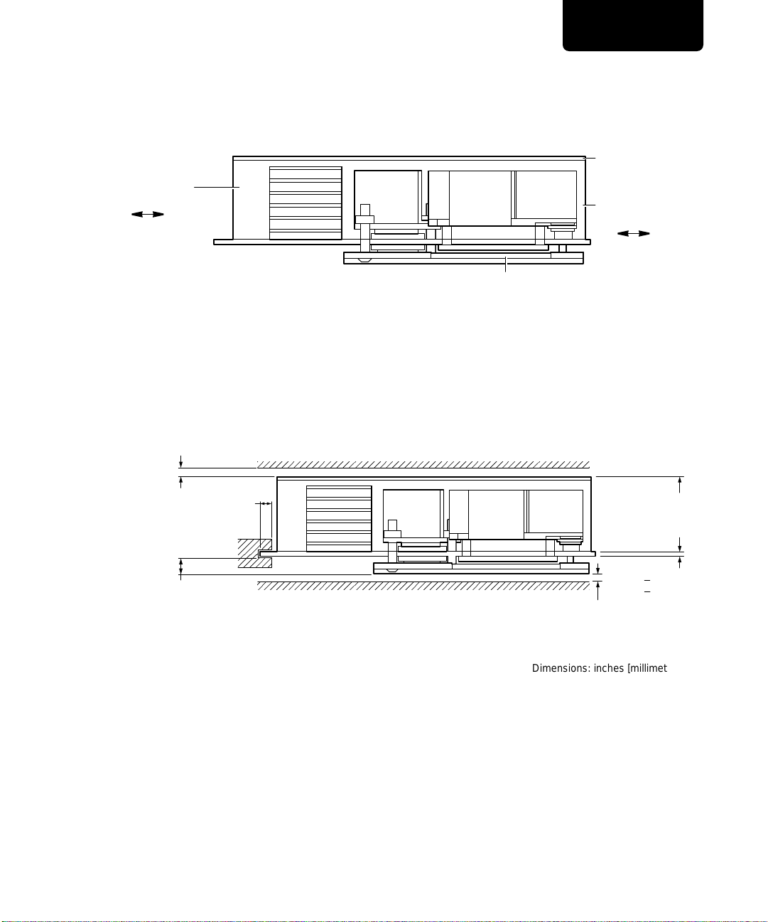
Bidirectional
Airflow
™
UltraSPARC
400 MHz CPU, 4.0 MB E-Cache
-II CPU Module
Figure 8. CPU Module Side View
Advanced Version
SME5224AUPA-400
Module
Shroud
Bidirectional
Airflow
Backside SRAM
Heat sink
Provide Minimum Frontside Clearance
0.079 [2.00]
Maximum Card Guide Depth
0.087 [2.201]
0.062 + 0.008
0.298
[7.57] Maximum
0.079 [2.00] Backside Clearance
Dimensions: inches [millimeters]
[1.57 + 0.20]
Provide Minimum
Figure 9. CPU Module Side View Dimensions
NOTE: A minimum backside clearance is required for airflow cooling of the backside heatsink.
1.318
[33.48]
Maximum
July 1999
Sun Microsystems, Inc
17
Page 46

™
UltraSPARC
SME5224AUPA-400 400 MHz CPU, 4.0 MB E-Cache
-II CPU Module
THERMAL SPECIFICATIONS
The maximum CPU operating frequencyand I/O timing is reduced when the junction temperature (Tj) of the
CPU device is raised. Airflow must be directed to the CPU heatsink to keep the CPU device cool. Correct airflow maintains the junctiontemperature withinits operating range. The airflow directed to the CPU is usually
sufficient to keep the surrounding devices on the topside of the module cool, including the SRAMs and clock
circuitry. The cooling of the backside SRAMs is less critical, but still requires airflow according to the specifications found in the section "Airflow Bottomside," on page 20.
The CPU temperature specification is provided in terms of its junction temperature. It is related to the case
temperature by the thermal resistance of the package and the power the CPU is dissipating.
The case temperature can be measured directly by a thermocouple probe, verifying that the CPU junction
temperature is correctly maintained over the entire operating range of the system. This includes both the
compute load and the environmental conditions for the system. If measuring the case temperature is problematic, then, measure the heatsink temperature and calculate the junction temperature. Both approaches for
calculating junction temperature are explained in this section. Irrespective of which method is used, accurate
measurement is required.
Two Step Approach to Thermal Design
Step One determines the ducted airflow requirements based on the CPU power dissipation, the thermal characteristics of the CPU package, and the surrounding heatsink assembly.
See "Thermal Definitions and Specifications," on page 19 for the modules specifications. The specifications for
the heatsinks are found in the table "Heatsink-to-Air Thermal Resistance," page 20.
Step Two verifies the cooling effectiveness of the design, by measuring the heatsink or case temperature
and calculating the junction temperature. The junction temperature must not exceed the CPU specification.
In addition, the lower the junction temperature, the higher the system reliability. The CPU temperature
must be verified under a range of system compute loads and system environmental conditions, using one of
the temperature measuring methods described herein.
18
Sun Microsystems, Inc
July 1999
Page 47

™
UltraSPARC
400 MHz CPU, 4.0 MB E-Cache
-II CPU Module
Thermal Definitions and Specifications
Term Definition Specification Comments
Tj Maximum device
junction
temperature
Tc Maximum case
temperature
Ts Heatsink
temperature
Ta Module ambient air
temperature
Pd Typical power
dissipation of the
CPU
θjc Maximum
junction-to-case
thermal resistance
of the package
θcs Case-to-heatsink
thermal resistance
θsa Heatsink-to-air
thermal resistance
Va Air velocity see page 20 The ducted airflow.
85 °C, The Tj can't be measured directly by a thermo-couple
probe. It must always be estimated as Tj or less. Less is
preferred.
76.7 °C Measurable at the top-center of the device. Requires a hole
in the base of the heatsink to allow the thermocouple to be
in contact with the case. Maximum case temperature is
specified using a CPU device at its maximum power
dissipation.
75 °C Measurable at the temperature of the base of the heatsink.
The best approach is to embed a thermocouple in a cavity
drilled in the heatsink base. An alternative approach is to
place the thermocouple between the fins/pins of the heatsink (insulated from the airflow) and in contact with the
base plate of the heatsink.
see page 20 The air temperature as it approaches the heatsink.
19.0 W The worst case compute loads over the entire process
range.
0.5°C/W The specification for the UltraSPARC™–II, 400 MHz CPU
in a ceramic LGA package.
0.1 °C/W Accuracy of thisvalue requiresthat good thermal contact is
made between the package and the heatsink.
see page 20 This value is dependent on the heatsink design, the airflow
direction, and the airflow velocity.
Advanced Version
SME5224AUPA-400
July 1999
Sun Microsystems, Inc
19
Page 48

™
UltraSPARC
SME5224AUPA-400 400 MHz CPU, 4.0 MB E-Cache
-II CPU Module
Temperature Estimating and Measuring Methods
The following methods can be used to estimate air cooling requirements and calculate junction temperature
based on thermo-couple temperature measurements.
Airflow Cooling Measurement Method
The relationship between air temperature and junction temperature is described in the following thermal
equation:
Tj = Ta + [Pd (θjc + θcs + θsa)]
Note: Testing is done with the worst-case power draw, software loading, and ambient air temperature.
Determination of the ambient air temperature (Ta) and the “free-stream” air velocity is required in order to
apply the airflow method. The table "Heatsink-to-Air Thermal Resistance," illustrates the thermal resistance
between the heatsink and air (θsa).
Note that the airflow velocity can be measured using a velocity meter. Alternatively it may be determined by
knowing the performance of the fan that is supplying the airflow. Calculating the airflow velocity is difficult.
It is subject to the interpretation of the term “free-stream.”
Note: The Airflow Cooling Estimate method is an estimate. Use it solely when an approximate value
suffices. Accuracy can only be assured using the Case Temperature measuring method or the
Heatsink Temperature measuring method. Apply these methods to insure a reliable performance.
"Heatsink-to-Air Thermal Resistance," specifies the thermal resistance of the heatsink as a function of the air
velocity.
Heatsink-to-Air Thermal Resistance
Air Velocity
θ
(°C/W)
SA
1. Ducted airflow through the heatsinks.
2. Airflow direction parallel to the shorter axis of the pin-fin heatsink (1.9"L x 3.6"W x 1.1"H)
(ft/min)
[1]
[2]
150 200 300 400 500 650 800 1000
1.21 1.05 0.91 0.84 0.78 0.72 0.67 0.64
Air Velocity Specifications
These specifications are recommended for a typical configuration:
Airflow Topside
150 LFM @ 30 °C up to 2,000 feet, altitude, maximum
300 LFM @ 40 °C up to 10,000 feet, altitude, maximum
Airflow Bottomside
100 LFM @ 30 °C up to 2,000 feet, altitude, maximum
150 LFM @ 40 °C up to 10,000 feet, altitude, maximum
20
Sun Microsystems, Inc
July 1999
Page 49

™
UltraSPARC
400 MHz CPU, 4.0 MB E-Cache
-II CPU Module
Advanced Version
SME5224AUPA-400
Case Temperature Measuring Method
The relationship between case temperature and junction temperature is described in the following thermal
equation.
If Tc is known, then Tj can be calculated:
Tj = Tc + (Pd x θjc)
Note: Testing is done with the worst-case power draw, software loading, and ambient air temperature.
There is good tracking between the case temperature and the heatsink temperature.
Heatsink Temperature Measuring Method
Measuring the heatsink temperature is sometimes easier than measuring the case temperature. This method
provides accurate results for most designs. If the heatsink temperature (Ts) is known then the following thermal equation can be used to estimate the junction temperature:
Tj = Ts + [Pd (θjc + θcs)]
July 1999
Sun Microsystems, Inc
21
Page 50

™
UltraSPARC
-II CPU Module
SME5224AUPA-400 400 MHz CPU, 4.0 MB E-Cache
JTAG TESTABILITY
The UltraSPARC™–II, 400 MHz CPU, 4.0 Mbyte module, (SME5224AUPA-400), implements the IEEE 1149.1
standard to aid in board level testing. Boundary Scan Description Language (BSDL) files are available for all
the active devices on the module, except the clock buffer.
AC Characteristics - JTAG Timing
400 MHz CPU
10 MHz TCK
Symbol Parameter Signals Conditions
tW(TRST) Test reset pulse width TRST
[1]
–– – ns
tSU(TDI) Input setup time to TCK TDI – 3 – ns
tSU(TMS) Input setup time to TCK TMS – 4 – ns
tH(TDI) Input hold time to TCK TDI – 1.5 – ns
tH(TMS) Input hold time to TCK TMS – 1.5 – ns
tPD(TDO) Output delay from TCK
tOH(TDO) Output hold time from TCK
1. TRST is an asynchronous reset.
2. TDO is referenced from falling edge of TCK.
[2]
TDO IOL = 8 mA
[2]
TDO 3 – – ns
I
OH
C
L
V
LOAD
= -4 mA
= 35 pF
= 1.5V
–6 – ns
UnitsMin Typ Max
22
Sun Microsystems, Inc
July 1999
Page 51

JTAG (IEEE 1149.1) TIMING
Data Input
Figure 10. Voltage Waveforms - Setup and Hold Times
In-Phase
Out-of-Phase
Clock
Clock
Output
Output
™
UltraSPARC
-II CPU Module
400 MHz CPU, 4.0 MB E-Cache
V
2.0V
t
t
H
SU
1.5V
1.5V
2.0V
t
PD
t
OH
t
OH
2.0V
0.8V
t
PD
0.8V
IH
V
IL
V
IH
V
IL
V
IH
V
IL
V
OH
V
OL
V
OH
V
OL
Advanced Version
SME5224AUPA-400
July 1999
Figure 11. Voltage Waveforms - Propagation Delay Times
Sun Microsystems, Inc
23
Page 52

™
UltraSPARC
-II CPU Module
SME5224AUPA-400 400 MHz CPU, 4.0 MB E-Cache
UPA CONNECTOR PIN ASSIGNMENTS (TOP VIEW)
(Pin 4) UP A_ADDR[1]
(Pin 10) UP A_ADDR[3]
UP A_ADDR[5]
UP A_ADDR[7]
UP A_ADDR[17]
UP A_ADDR[19]
UP A_ADDR[21]
UP A_ADDR[23]
UP A_ADDR[33]
UP A_RATIO
UP A_P_REPLY[0]
UP A_P_REPLY[2]
UP A_CLK0_POS
TEMP_SENSE_NEG
UP A_S_REPLY[0]
UP A_S_REPLY[2]
UP A_ECC[11]
UP A_ECC[9]
UP A_D ATA[87]
UP A_D ATA[85]
UP A_D ATA[83]
(Pin 136) UP A_D ATA[81]
(Pin 142) UP A_D ATA[71]
(Pin 148) UP A_D ATA[69]
(Pin 154) UP A_D ATA[67]
UP A_D ATA[65]
UP A_D ATA[119]
UP A_D ATA[117]
UP A_D ATA[115]
UP A_D ATA[113]
UP A_D ATA[103]
UP A_D ATA[101]
UP A_D ATA[99]
UP A_D ATA[97]
UP A_ECC[3]
UP A_ECC[1]
UP A_D ATA[55]
UP A_D ATA[53]
UP A_D ATA[51]
UP A_D ATA[49]
UP A_D ATA[39]
UP A_D ATA[37]
UP A_D ATA[35]
UP A_D ATA[33]
UP A_D ATA[23]
UP A_D ATA[21]
UP A_D ATA[19]
UP A_D ATA[17]
UP A_D ATA[7]
UP A_D ATA[5]
UP A_D ATA[3]
UP A_D ATA[1]
(Pin 322) UP A_ECC_VALID
(Pin 328) CPU_CLK_NEG
(Pin 1) UP A_ADDR[0]
(Pin 7) UP A_ADDR[2]
UP A_ADDR[4]
UP A_ADDR[6]
UP A_ADDR[16]
UP A_ADDR[18]
UP A_ADDR[20]
UP A_ADDR[22]
UP A_ADDR[32]
UP A_ADDR[34]
UP A_REQ_IN[2]
UP A_P_REPLY[1]
TDI
UP A_CLK0_NEG
TEMP_SENSE_POS
UP A_POR T_ID[0]
UP A_S_REPLY[1]
UP A_SPEED[0]
UP A_ECC[10]
UP A_D ATA[86]
UP A_D ATA[84]
(Pin 133) UP A_D ATA[82]
(Pin 139) UP A_D ATA[80]
(Pin 145) UP A_D ATA[70]
(Pin 151) UP A_D ATA[68]
UP A_D ATA[66]
UP A_D ATA[64]
UP A_D ATA[118]
UP A_D ATA[116]
UP A_D ATA[114]
UP A_D ATA[112]
UP A_D ATA[102]
UP A_D ATA[100]
UP A_D ATA[98]
UP A_D ATA[96]
UP A_D ATA[54]
UP A_D ATA[52]
UP A_D ATA[50]
UP A_D ATA[48]
UP A_D ATA[38]
UP A_D ATA[36]
UP A_D ATA[34]
UP A_D ATA[32]
UP A_D ATA[22]
UP A_D ATA[20]
UP A_D ATA[18]
UP A_D ATA[16]
(Pin 319) UP A_D ATA[0]
(Pin 325) CPU_CLK_POS
UP A_XIR_L
UP A_ECC[8]
UP A_ECC[2]
UP A_ECC[0]
UP A_D ATA[6]
UP A_D ATA[4]
UP A_D ATA[2]
Pin 1
GND (Pin 2)
VDD (Pin 8)
GND
VDD_CORE
GND
GND
GND
GND
VDD_CORE
GND
VDD_CORE
GND
GND
GND
POWER_0V
VDD_CORE
GND
VDD_CORE
GND
GND
GND
GND
VDD_CORE (Pin 134)
GND (Pin 140)
VDD_CORE (Pin 146)
GND (Pin 152)
GND
GND
GND
VDD_CORE
GND
VDD
GND
GND
GND
GND
VDD
GND
VDD
GND
GND
GND
GND
VDD
GND
VDD
GND
GND
GND
GND
VDD
GND
VDD
GND (Pin 320)
GND (Pin 326)
GND (Pin 5)
GND (Pin 11)
GND
GND
VDD_CORE
GND
VDD_CORE
GND
GND
GND
GND
VDD_CORE
GND
VDD_CORE
UP A_POR T_ID[1]
GND
GND
GND
VDD_CORE
GND
VDD_CORE
GND
GND (Pin 137)
GND (Pin 143)
GND (Pin 149)
VDD_CORE (Pin 155)
GND
VDD_CORE
GND
GND
GND
GND
VDD
GND
VDD
GND
GND
GND
GND
VDD
GND
VDD
GND
GND
GND
GND
VDD
GND
VDD
GND
GND
GND
GND
VDD (Pin 323)
GND (Pin 329)
24
Sun Microsystems, Inc
July 1999
Page 53

UltraSPARC
400 MHz CPU, 4.0 MB E-Cache
UPA CONNECTOR PIN ASSIGNMENTS (BOTTOM VIEW)
(Pin 5) GND
(Pin 11) GND
GND
GND
VDD_CORE
GND
VDD_CORE
GND
GND
GND
GND
VDD_CORE
GND
VDD_CORE
UP A_POR T_ID[1]
GND
GND
GND
VDD_CORE
GND
VDD_CORE
GND
(Pin 137) GND
(Pin 143) GND
(Pin 149) GND
(Pin 155) VDD_CORE
GND
VDD_CORE
GND
GND
GND
GND
VDD
GND
VDD
GND
GND
GND
GND
VDD
GND
VDD
GND
GND
GND
GND
VDD
GND
VDD
GND
GND
GND
GND
(Pin 323) VDD
(Pin 329) GND
Pin 3
(Pin 2) GND
(Pin 8) VDD
GND
VDD_CORE
GND
GND
GND
GND
VDD_CORE
GND
VDD_CORE
GND
GND
GND
POWER_0V
VDD_CORE
GND
VDD_CORE
GND
GND
GND
(Pin 134) VDD_CORE
(Pin 146) VDD_CORE
GND
(Pin 140) GND
(Pin 152) GND
GND
GND
GND
VDD_CORE
GND
VDD
GND
GND
GND
GND
VDD
GND
VDD
GND
GND
GND
GND
VDD
GND
VDD
GND
GND
GND
GND
VDD
GND
VDD
(Pin 320) GND
(Pin 326) GND
UP A_ADDR[8] (Pin 3)
UP A_ADDR[10] (Pin 9)
UP A_ADDR[12]
UP A_ADDR[14]
UP A_ADDR[24]
UP A_ADDR[26]
UP A_ADDR[28]
UP A_ADDR[30]
UP A_ADDR[35]
UP A_REQ_OUT
UP A_REQ_IN[1]
UP A_P_REPLY[4]
UP A_D ATA_STALL
TRST_L
POWER_SET_NEG
UP A_RESET_L
UP A_S_REPLY[4]
UP A_SPEED[1]
UP A_ECC[14]
UP A_ECC[12]
UP A_D ATA[94]
UP A_D ATA[92]
UP A_D ATA[90] (Pin 135)
UP A_D ATA[88] (Pin 141)
UP A_D ATA[78] (Pin 147)
UP A_D ATA[76] (Pin 153)
UP A_D ATA[74]
UP A_D ATA[72]
UP A_D ATA[126]
UP A_D ATA[124]
UP A_D ATA[122]
UP A_D ATA[120]
UP A_D ATA[110]
UP A_D ATA[108]
UP A_D ATA[106]
UP A_D ATA[104]
UP A_ECC[6]
UP A_ECC[4]
UP A_D ATA[62]
UP A_D ATA[60]
UP A_D ATA[58]
UP A_D ATA[56]
UP A_D ATA[46]
UP A_D ATA[44]
UP A_D ATA[42]
UP A_D ATA[40]
UP A_D ATA[30]
UP A_D ATA[28]
UP A_D ATA[26]
UP A_D ATA[24]
UP A_D ATA[14]
UP A_D ATA[12]
UP A_D ATA[10]
UP A_D ATA[8] (Pin 321)
UP A_CLK1_POS (Pin 327)
™
-II CPU Module
UP A_ADDR[9] (Pin 6)
UP A_ADDR[11] (Pin 12)
UP A_ADDR[13]
UP A_ADDR[15]
UP A_ADDR[25]
UP A_ADDR[27]
UP A_ADDR[29]
UP A_ADDR[31]
UP A_ADDR_VALID
UP A_REQ_IN[0]
UP A_P_REPLY[3]
UP A_SC_REQ_IN
TCK
POWER_SET_POS
TMS
UP A_S_REPLY[3]
UP A_SPEED[2]
UP A_ECC[15]
UP A_ECC[13]
UP A_D ATA[95]
UP A_D ATA[93]
UP A_D ATA[91]
UP A_D ATA[89] (Pin 138)
UP A_D ATA[79] (Pin 144)
UP A_D ATA[77] (Pin 150)
UP A_D ATA[75] (Pin 156)
UP A_D ATA[73]
UP A_D ATA[127]
UP A_D ATA[125]
UP A_D ATA[123]
UP A_D ATA[121]
UP A_D ATA[111]
UP A_D ATA[109]
UP A_D ATA[107]
UP A_D ATA[105]
UP A_ECC[7]
UP A_ECC[5]
UP A_D ATA[63]
UP A_D ATA[61]
UP A_D ATA[59]
UP A_D ATA[57]
UP A_D ATA[47]
UP A_D ATA[45]
UP A_D ATA[43]
UP A_D ATA[41]
UP A_D ATA[31]
UP A_D ATA[29]
UP A_D ATA[27]
UP A_D ATA[25]
UP A_D ATA[15]
UP A_D ATA[13]
UP A_D ATA[11]
UP A_D ATA[9]
TDO (Pin 324)
UP A_CLK1_NEG (Pin 330)
Advanced Version
SME5224AUPA-400
July 1999
Sun Microsystems, Inc
25
Page 54

™
UltraSPARC
SME5224AUPA-400 400 MHz CPU, 4.0 MB E-Cache
-II CPU Module
STORAGE AND SHIPPING SPECIFICATION
Value
Parameter Conditions
Temperature Ambient -40 – 90 °C
Temperature ramp Ambient – – 10 °C/min.
Shock (shipping)
- single module package
Shock(shipping)
- multi-module package
Drop height on to any edge, corner, or side of
shipping box
Drop height on to any edge, corner, or side of
shipping box
– – 21 inches
– – 18 inches
UnitMin. Typ. Max
HANDLING CPU MODULES
CAUTION: Handle a module by carefully holding it by its edges and by the large CPU heatsink. Do not
bump or handle the SRAM heatsinks because this action can cause unseen damage to the solder connections.
Always handle modules and other electronic devices in an ESD-controlled environment.
26
Sun Microsystems, Inc
July 1999
Page 55

™
UltraSPARC
-II CPU Module
400 MHz CPU, 4.0 MB E-Cache
Advanced Version
SME5224AUPA-400
ORDERING INFORMATION
Part Number CPU Speeds Description
SME5224AUPA-400 400 MHz CPU The UltraSPARC™–II, 400 MHz CPU, 4.0 Mbyte module, features the UltraSPARC-II
1. To order the data sheet for this device use the document part number: 805-6390-05
[1]
CPU at 400 MHz, a 4.0 Mbyte external cache, and two UDB-II data buffer ASICs.
DOCUMENT REVISION HISTORY
Date Document No. Change
July 1999 805-4835-05 This module is designed using the the UltraSPARC™–II, 400 MHz CPU,
May 1999 805-6390-04 Re-organization of the datasheet and update of specifications.
March 1999 805-6390-03
Preliminary Version
December 1998 805-6390-02
Advanced Version
revision 3.x. See page 9, "Module Clocks," for changes effecting this version of
the module.
New section concerning the System Timing and Thermal Specifications.
Revised specifications for DC characteristics and module power consumption.
Illustrations reflect a new heat sink design. Thermal section reflects the latest
heatsink design.
July 1999
Sun Microsystems, Inc
27
Page 56

SME5224AUPA-400
Sun Microsystems, Inc.
901 San Antonio Road
Palo Alto, CA 94303-4900 USA
800/681-8845
www.sun.com/microelectronics
©1999 Sun Microsystems, Inc. All Rights reserved.
THE INFORMATION CONTAINED IN THIS DOCUMENT IS PROVIDED “AS IS” WITHOUT ANY EXPRESS REPRESENTATIONS OF WARRANTIES. IN
ADDITION, SUN MICROSYSTEMS, INC. DISCLAIMS ALL IMPLIED REPRESENTATIONS AND WARRANTIES, INCLUDING ANY WARRANTY OF
MERCHANTABILITY, FITNESS FOR A PARTICULAR PURPOSE, OR NON-INFRINGEMENT OF THIRD PARTY INTELLECTURAL PROPERTY RIGHTS.
This document contains proprietary information of Sun Microsystems, Inc. or under license from third parties. No part of this document may be reproduced
in any form or by any means or transferred to any third party without the prior written consent of Sun Microsystems, Inc.
Sun, Sun Microsystems, the Sun Logo, Ultra, and VIS are trademarks or registered trademarks of Sun Microsystems, Inc. in the United States and other
countries. All SPARC trademarks are used under license and are trademarks or registered trademarks of SPARC International, Inc. in the United States and
other countries. Products bearing SPARC trademarks are based upon an architecture developed by Sun Microsystems, Inc.
The information contained in this document is not designed or intended for use in on-line control of aircraft, aircraft navigation or aircraft communications;
or in the design, construction, operation or maintenance of any nuclear facility. Sun disclaims any express or implied warranty of fitness for such uses.
Part Number: 805-6390-05
 Loading...