

Page 1

TM – 8120000501
3131 SW 42nd Street, Fort Lauderdale, Florida 33312 U.S.A.
http://www.sunairelectronics.com
1 KW DIGITAL
ANTENNA COUPLER
CU-9150
Operation and Maintenance Manual (Rev. C)
Page 2

CU-9150
Proprietary/Confidentiality Notice
The information disclosed in this document, including all designs and related materials, is the
property of RIIMIC LLC dba (doing business as) Sunair Electronics (hereinafter “Sunair”)
and/or its licensors. Sunair and/or its licensors reserve all patent, copyright, and other proprietary
rights to this document, including all design, manufacturing, reproduction, use, and sales rights
thereto, except to the extent said rights are expressly granted to others. Reproduction of this
document or portions thereof without prior written approval of Sunair is prohibited.
Return Material Authorization (RMA) Procedures
In case of difficulty, please contact the Sunair Product Service Department between the hours of
8:30 a.m. and 5:30 p.m. EST.
Telephone: (954) 400-5100
Fax: (954) 583-7337
Email: [email protected]
To return an item for repair or replacement, a Return Material Authorization (RMA) is required
from the Product Service Department. When you receive the RMA number, carefully pack the
item(s) and ship the package(s) to the address provided by your Product Service Representative.
Write the RMA number in a visual location on the outside of the shipping container.
Retain a copy of all information sheets included with the packaging.
ii Use or disclosure of information from this document is subject to the restrictions
indicated on the proprietary/confidentiality page of this document.
Page 3

CU-9150
Warranty Policy
Ground and Marine Products
Sunair Electronics warrants each piece of equipment manufactured by it to be free from defects
in material and workmanship, under normal use for the lesser of one (1) year from the date of
installation or 15 months from the date of shipment from Sunair.
Sunair will repair or replace, at its option, any defective equipment or component of the
equipment returned to it at its factory, transportation prepaid, within such warranty period. No
reimbursement will be made for non-factory repair charges.
This warranty is void if equipment is modified or repaired without authorization, subject to
misuse, abuse, accident, water damage or other neglect, or has its serial number defaced or
removed.
THIS WARRANTY IS ESPECIALLY IN LIEU OF ANY AND ALL OTHER WARRANTIES
EXPRESSED OR IMPLIED, INCLUDING ANY IMPLIED WARRANTY OF
MERCHANTABILITY OR FITNESS FOR A PARTICULAR PURPOSE. The obligation and
responsibility of Sunair shall be limited to that expressly provided herein and Sunair shall not be
liable for consequential or other damage or expense whatsoever therefore or by any reason
thereof.
Sunair reserves the right to make changes in the design or additions to or improvements in its
equipment without obligation to install such additions or improvements in equipment theretofore
manufactured.
Training
Sunair offers training programs of varying lengths covering operation, service and maintenance
of all Sunair manufactured equipment. For details please contact the Product Service
Department.
Use or disclosure of information from this document is subject to the restrictions iii
indicated on the proprietary/confidentiality page of this document.
Page 4

CU-9150
Revision
Page(s)
Manual
Revision
Date
Unit Serial No.
Effectivity
Addendum
Covered
B
Page changes 1:
05/27/98
Page changes 2:
07/15/98
Page changes 3:
08/24/99
Page changes 4:
06/25/03
C
3/22/2011
Reformatted to current
standards. This includes new
numbers for Figures and
Tables.
All
Added temperatures in
Fahrenheit.
1-2
Updated the contact
information with the new
address and phone numbers.
i, ii, 2-1, 2-2
Re-created some of the hand-
drawn diagrams using
illustrating software.
2-6, 2-8,
2-10,
Revision Record
Copyright © 1998, 1999, 2003, 2011 by Sunair Electronics Inc.
All rights reserved.
No part of this publication may be reproduced, stored in a retrieval system, or transmitted in any form or by any
means, electronic, mechanical, photocopying, recording, or otherwise, without the prior written permission of Sunair
Electronics, Inc.
iv Use or disclosure of information in this document is subject to the restrictions
indicated on the proprietary/confidentiality page of this document.
Page 5

CU-9150
Table of Contents
1.0 General Information ............................................................................................................................ 1-1
1.1 Scope of Manual ........................................................................................................................ 1-1
1.2 General Description ................................................................................................................... 1-1
1.2.1 Assemblies .................................................................................................................... 1-1
1.3 Technical Specifications ............................................................................................................ 1-2
1.3.1 General ......................................................................................................................... 1-2
1.3.2 Environmental .............................................................................................................. 1-2
1.4 Equipment Supplied .................................................................................................................. 1-3
1.5 Equipment Required, Not Supplied ........................................................................................... 1-3
1.6 Optional Equipment ................................................................................................................... 1-4
2.0 Installation ........................................................................................................................................... 2-1
2.1 General....................................................................................................................................... 2-1
2.2 Unpacking and Inspection ......................................................................................................... 2-1
2.3 Return of Equipment to Factory ................................................................................................ 2-1
2.4 Power Requirements .................................................................................................................. 2-2
2.5 Installation Considerations and Mounting Information ............................................................. 2-2
2.5.1 General Installation Procedures and Requirements ...................................................... 2-2
2.5.2 Mounting Considerations ............................................................................................. 2-3
2.5.3 Installation of Remote Control and RF Cables ............................................................. 2-3
2.6 Antennas and Ground Systems .................................................................................................. 2-3
2.6.1 General ......................................................................................................................... 2-3
2.6.2 Random Length Non-Resonant Antennas .................................................................... 2-4
2.7 Long-Wire Adapter Kit (1A1A5) 8120909003 ......................................................................... 2-4
2.8 TX Only Function ...................................................................................................................... 2-5
2.9 Software Revision ...................................................................................................................... 2-5
2.10 Checks after Installation ............................................................................................................ 2-5
2.11 Integration with Third Party Radio Systems.............................................................................. 2-5
3.0 Operation ............................................................................................................................................. 3-1
3.1 General....................................................................................................................................... 3-1
3.2 Operating the CU-9150 ............................................................................................................. 3-1
3.2.1 Operation with 9000 Series Exciters/Transceivers and LPA-9600 .............................. 3-1
3.2.2 1000 Watt Operational Checkout ................................................................................. 3-1
4.0 Theory of Operation ............................................................................................................................ 4-1
4.1 General....................................................................................................................................... 4-1
4.2 Antenna Impedance Matching Network .................................................................................... 4-1
4.3 Chassis Assembly 1A1 .............................................................................................................. 4-2
4.3.1 General ......................................................................................................................... 4-2
4.4 Input Connector Assembly 1A1A2 ........................................................................................... 4-2
Use or disclosure of information from this document is subject to the restrictions v
indicated on the proprietary/confidentiality page of this document.
Page 6

CU-9150
Table of Contents
4.4.1 General ......................................................................................................................... 4-2
4.4.2 Configuration and Operation ........................................................................................ 4-2
4.5 CPU Assembly 1A1A3 .............................................................................................................. 4-2
4.5.1 General ......................................................................................................................... 4-2
4.5.2 Microprocessor ............................................................................................................. 4-2
4.5.3 Serial Communication .................................................................................................. 4-3
4.5.4 A/D Converter .............................................................................................................. 4-3
4.5.5 Relay Drivers ................................................................................................................ 4-3
4.5.6 Channel Change and Tune Command Detectors .......................................................... 4-3
4.6 RF Detector Assembly 1A1A4A1 ............................................................................................. 4-4
4.6.1 General ......................................................................................................................... 4-4
4.6.2 Magnitude Discriminator .............................................................................................. 4-4
4.6.3 Phase Discriminator...................................................................................................... 4-4
4.6.4 Attenuator Pad, -3 dB ................................................................................................... 4-5
4.6.5 50 Ohm Calibration Termination ................................................................................. 4-5
4.6.6 TX Only Function......................................................................................................... 4-5
4.7 Input Capacitor Assembly 1A1A4A2 ........................................................................................ 4-6
4.7.1 General ......................................................................................................................... 4-6
4.7.2 Configuration and Operation ........................................................................................ 4-6
4.8 Mother Board Assembly 1A1A1 ............................................................................................... 4-6
4.8.1 General ......................................................................................................................... 4-6
4.8.2 DC Power ..................................................................................................................... 4-6
4.8.3 Series L and Shunt C Relays ........................................................................................ 4-6
4.8.4 L-OUT Relays .............................................................................................................. 4-6
4.9 Interface Requirements for Third Party Equipment .................................................................. 4-7
4.9.1 Signal Descriptions ....................................................................................................... 4-7
5.0 General ................................................................................................................................................ 5-1
5.1 Preventive Maintenance............................................................................................................. 5-1
5.1.1 Gasket Replacement ..................................................................................................... 5-1
5.2 Disassembly ............................................................................................................................... 5-2
5.2.1 Cover Removal ............................................................................................................. 5-2
5.2.2 CPU Removal ............................................................................................................... 5-2
5.2.3 RF Detector/Input Capacitor Removal ......................................................................... 5-4
5.2.4 Chassis Removal .......................................................................................................... 5-4
5.3 Indicators ................................................................................................................................... 5-5
5.4 Test Equipment Required or Equivalent .................................................................................... 5-6
5.5 Alignment and Checks ............................................................................................................... 5-6
5.6 Troubleshooting ......................................................................................................................... 5-8
vi Use or disclosure of information from this document is subject to the restrictions
indicated on the proprietary/confidentiality page of this document.
Page 7

CU-9150
Table of Contents
5.6.1 Coupler Will Not Tune - No Relay Action - No Tuning Fault ..................................... 5-8
5.6.2 Coupler Will Not Tune - No Relay Action - Tuning Fault Indicated ........................... 5-9
5.6.3 Relays Operate But Tuning Fault Indicated ................................................................. 5-9
5.6.4 Coupler Tunes but Memory Does Not Work ............................................................... 5-9
5.7 DIP Switch Settings ................................................................................................................... 5-9
6.0 Options ................................................................................................................................................ 6-1
6.1 Diagnostic Test Set .................................................................................................................... 6-1
6.1.1 General Information ..................................................................................................... 6-1
6.1.2 Test Set Operation ........................................................................................................ 6-2
6.2 CU-9150H Serial Control Upgrade ......................................................................................... 6-31
6.2.1 General Information ................................................................................................... 6-31
6.2.2 Installation .................................................................................................................. 6-31
6.2.3 Operation .................................................................................................................... 6-32
6.2.4 Theory ........................................................................................................................ 6-35
6.2.5 Troubleshooting .......................................................................................................... 6-36
Use or disclosure of information from this document is subject to the restrictions vii
indicated on the proprietary/confidentiality page of this document.
Page 8

CU-9150
Listing of Figures
Figure 2.11-1. CU-9150 Control Cable P/N 8092500096 ........................................................................ 2-6
Figure 2.11-2. Coupler Outline Dimensions ............................................................................................. 2-7
Figure 2.11-3. LPA-9600 with CU-9150, 35-Foot Antenna (Roof Top Installation) ............................... 2-9
Figure 2.11-4. LPA-9600 with CU-9150, Non-Resonant Antenna ........................................................ 2-10
Figure 2.11-5. Longwire Antenna Kit ..................................................................................................... 2-11
Figure 2.11-6. Long-Wire Adapter Kit (1A1A5) 81200909003 Installation Configured for Long-Wire
Operation ........................................................................................................................................... 2-12
Figure 2.11-7. Long-Wire Adapter Kit (1A1A5) 81200909003 Installation Configured for Whip Wire
Operation ........................................................................................................................................... 2-12
Figure 2.11-8. Assembly/Disassembly of Antenna Output Lead (Long-Wire Adapter Kit Not Installed)2-13
Figure 4.9-1. Coupler Interface Timing .................................................................................................... 4-9
Figure 4.9-2. CU-9150 Assembly Tree ................................................................................................... 4-10
Figure 4.9-3. CU-9150 Block Diagram .............................................................................................. 4-11
Figure 5.2-1. Gasket Installation and Torque Sequence ........................................................................... 5-3
Figure 5.2-2 Chassis Removal .................................................................................................................. 5-5
Figure 5.5-1. 1A1A4A1 RF Detector Alignment Adjustment Locations ................................................. 5-7
Figure 5.7-1 CU-9150 Assembly Locations ........................................................................................... 5-11
Figure 5.7-2 1A1 Chassis Component Locations ................................................................................... 5-12
Figure 5.7-3. Non-Chassis Component Locations .................................................................................. 5-13
Figure 5.7-4. Final Assembly Tested CU-9150, Chassis Assembly 1A1 and Long Wire Adapter Kit
1A1A5 ............................................................................................................................................... 5-15
Figure 5.7-5. PC Assembly, CU-9150 Motherboard, 1A1A1 ................................................................. 5-17
Figure 5.7-6. PC Assembly, Input Connector, 1A1A2 ........................................................................... 5-21
Figure 5.7-7. PC Assembly, CPU, 1A1A3 ............................................................................................. 5-23
Figure 5.7-8. PC Assembly, RF Detector, 1A1A4A1 ............................................................................. 5-33
Figure 5.7-9. PC Assembly, PC Assembly, Input Capacitor, 1A1A4A2 ................................................ 5-35
Figure 6.1-1. PC Assembly, Test Fixture, CU-9150 CPU ........................................................................ 6-9
Figure 6.1-2. PC Assembly, Serial Breakout Board ............................................................................... 6-19
Figure 6.1-3. PC Assembly, Display Board ............................................................................................ 6-21
viii Use or disclosure of information from this document is subject to the restrictions
indicated on the proprietary/confidentiality page of this document.
Page 9

CU-9150
Listing of Tables
Table 1.4-1 List of Equipment Supplied ................................................................................................... 1-3
Table 1.5-1 List of Equipment Required, Not Supplied ........................................................................... 1-3
Table 1.6-1. Optional Equipment .............................................................................................................. 1-4
Table 3.2-1. Acceptable Reflected Power Chart for VSWR 1.5:1. for LPA-9600 ................................... 3-2
Table 3.2-2. Acceptable Reflected Power Chart for VSWR 1.5:1. for LPA-9500 ................................... 3-2
Table 4.9-1. Signal List and Descriptions ................................................................................................. 4-7
Table 5.3-1. CU-9150 Indicators and Meanings ....................................................................................... 5-5
Table 5.7-1 S201 DIP Switch Settings.................................................................................................... 5-10
Table 5.7-2 CU-9150 Detailed Assemblies List ..................................................................................... 5-14
Table 6.1-1 Equipment Supplied .............................................................................................................. 6-1
Table 6.1-2 Coupler Operation Terms ...................................................................................................... 6-2
Table 6.1-3. Board Level Test Components Required .............................................................................. 6-2
Table 6.1-4 Serial Breakout Equipment Required .................................................................................... 6-6
Table 6.1-5. TuneView Parameters ........................................................................................................... 6-7
Table 6.2-1. CU-9150H Conversion Kit ................................................................................................. 6-31
Table 6.2-2. CU-9150H Control Cable Signals ...................................................................................... 6-32
Use or disclosure of information from this document is subject to the restrictions ix
indicated on the proprietary/confidentiality page of this document.
Page 10

CU-9150
*(asterisk) Selected function
ACC Automatic Carrier Control
ADDR Address
AFSK Audio Frequency-Shift Keying
AGC Automatic Gain Control
ALC Automatic Level Control
ALE Address Latch Enable
Automatic Link Establishment
AM Amplitude Modulation
AME Amplitude Modulation
Equivalent
AMP/AMPL Amplifier
ARQ Automatic Request
ATC Air Traffic Control
AUD Audio
AUTO Automatic
AUX Auxiliary
BAUD Variable unit of data
transmission speed (bits per
second)
BELL U.S. Telephone standards
BFO Beat Frequency Oscillator
BITE Built In Test Equipment
BRD Board
CH/CHAN/
CHL/CHN Channel
CLR Clear
CMOS Complementary Metal Oxide
Semiconductor
CPLR Coupler
CPU Central Processing Unit
(Computer)
CTCSS Continuous Tone Coded Squelch
System
CW Continuous Wave
dB Decibel
dBm Decibels referred to 1 milliwatt
DCS Digital Coded Squelch
DSBSC Double Sideband Suppressed
Carrier
DSP Display
Digital Signal Processor
DTMF Dual Tone Multi-Frequency
DUART Dual Asynchronous Receive/
Transmit
EEPROM Electrically Erasable and
Programmable Read Only Memory
EIA Electronics Industry Alliance
EL Electroluminescent
EMI Electromagnetic Immunity
EMP Electromagnetic Pulse
ENTR Enter
EPROM Eraseable Programmable Read Only
Memory
ESD Electrostatic Discharge
ETSI European Telecommunications
Standards Institute
FAX Facsimile
FEC Forward Error Correction
FM Frequency Modulation
FREQ Frequency
FSK Frequency Shift Keying
FWD Forward
GRP Group
HF High Frequency
HPAC High Power Amplifier Controller
Hz Hertz
IC Integrated Circuit
IF Intermediate Frequency
IMD Intermodulation Distortion
I/O Input/Output
IONCAP Ionospheric Communications
Analysis and Prediction (Program)
ISB Independent Sideband
kHz Kilohertz
kW Kilowatt
LCD Liquid Crystal Display
LCL Local
LED Light Emitting Diode
LK Link
LO Local Oscillator
LRU Lowest Repairable Unit
LSB Lower Sideband
LT Light
LVL Level
MIC Microphone
Abbreviations/Acronyms
x Use or disclosure of information from this document is subject to the restrictions
indicated on the proprietary/confidentiality page of this document.
Page 11

CU-9150
MAN Manual
M CH Manual Channel
MED Medium
MHz Megahertz
MED Medium
MHz Megahertz
MIC Microphone
MIL-STD Military Standard
MNL Manual
ms Millisecond
MTBF Mean Time Between Failures
MTR Meter
MTTR Mean Time To Repair
NAR Narrow
NB Narrow Band
PA Power Amplifier
P.C. Printed Circuit
PEP Peak Envelope Power
PLL Phase-Locked Loop
P/N Part Number
PNL Panel
POSTSL Post-Selector
PRESEL Pre-Selector
PTT Push-To-Talk
PWR Power
RCV Receive
REFD/REFL/
RFL Reflected
REV Revision
RF Radio Frequency
RFI Radio Frequency Interference
RMA Return Material Authorization
RMT Remote
RS232 Computer control, hardwired up
to 50 feet maximum
RS422 Computer control, hardwired up to 4000
feet maximum
RS485 Computer control, hardwired for
multiple users
RTTY Radio Teletype
RX Receive
RU Rack Unit
SDR Software Defined Radio
SEL Select
SINAD Signal to Noise and Distortion
SLO Slow
S MTR Signal Strength Meter
SPKR Speaker
SPLX Simplex
SRAM Static Random Access Memory
SSB Single Sideband
TCXO Temperature Compensated Crystal
Oscillator
TFT Thin Film Technology
TGC Transmit Gain Control
THD Total Harmonic Distortion
TTL Translator Transistor Logic
TX Transmit
USB Upper Sideband
UTC Universal Time Coordinated
VC Voltage Control
VCO Voltage Controlled Oscillator
VHF Very High Frequency
VRMS Volts Root Mean Square
VSWR Voltage Standing Wave Ratio
W Watt
WB Wide Band
WPM Words Per Minute
XMT Transmit
Abbreviations/Acronyms (Continued)
Use or disclosure of information from this document is subject to the restrictions xi
indicated on the proprietary/confidentiality page of this document.
Page 12

CU-9150
Electrical Safe Work Practices
Accidents involving electricity can cause burns, explosions, shocks, and death. Only trained and
qualified personnel should service, install, or repair electrical equipment.
The general safety procedures for personnel servicing electronic and electrical equipment
include:
1. Always turn off or disconnect power before working on electric equipment, electronic
circuits, or any type of electrical item.
2. Turn off and disconnect power before checking or replacing fuses.
3. Locate and correct the cause of a blown fuse or tripped circuit breaker before replacing
the fuse or resetting the circuit breaker.
4. Never defeat the purpose of a fuse or circuit breaker. Always install a fuse with the
correct amperage rating for the circuit. Never install a fuse with a higher rating.
5. Always have a second trained and qualified person present when working on electrical
systems (protected or unprotected).
6. Always remove metal jewelry, watches, rings, etc., before working on electrical circuits
or any electrical equipment.
7. Do not work on electrical equipment in a wet area. Never place containers of liquid on
electrical equipment.
8. Do not touch an object that may provide a hazardous path to earth ground.
9. Safely discharge capacitors in equipment before working on the circuits (refer to ESD
procedures).
10. Inspect cabling for defects, including frayed wiring, loose connections, or cracked
insulation. Replace defective cords and plugs.
11. Always check the electrical ratings of equipment and verify that the ratings are correct.
12. Never overload circuits.
13. Verify grounding of equipment chassis/cabinets. Never cut off or defeat the ground
connection on a plug.
14. When working at any site, always observe all safety signs and safety procedures. They
exist to protect personnel from injuries.
15. All persons working on or around electrical/electronic equipment should have first aid
training, including resuscitation procedures and external cardiac compression.
xii Use or disclosure of information from this document is subject to the restrictions
indicated on the proprietary/confidentiality page of this document.
Page 13

CU-9150
Electrostatic Discharge (ESD)
Electrostatic Discharge (ESD) can severely damage sensitive components located on printed
circuit cards. Electrostatic discharge measurements as high as 35,000 volts, can occur from
walking across a carpet.
To avoid potential damage to electronic equipment, follow correct electrostatic discharge
preventive procedures when handling or working with the hardware.
1. Always wear an electrostatic discharge wrist strap when handling electronic hardware.
2. Connect the electrostatic discharge wrist strap to a reliable earth ground.
3. Replace worn or frayed electrostatic discharge wrist straps and connecting cords.
4. Check your electrostatic discharge strap every month.
5. Do not use electrostatic discharge straps that are out of calibration.
6. Place printed circuit cards in an electrostatic discharge bag or other ESD container to
avoid damage from stray static charge.
7. Do not place printed circuit cards on any surface that is not an approved electrostatic
discharge surface correctly connected to earth ground.
8. Always handle printed circuit cards by the edges. Avoid touching any of the sensitive
circuits on the card.
Use or disclosure of information from this document is subject to the restrictions xiii
indicated on the proprietary/confidentiality page of this document.
Page 14

CU-9150
Hazardous Materials
Hazardous materials are likely to be present at the maintenance facility. Many of the following
substances are toxic (causing illness or death): flammable materials, explosive materials,
corrosive materials that cause the skin or eyes to burn on contact, reactive materials that, when
exposed to heat, air, water, or certain other chemicals, can cause burning or release of toxic
vapors.
Some hazardous substances are obvious, for example, adhesives, solvents, abrasives, fuels, and
pesticides. Other substances are less obvious, for example, toner in office copiers and printers
and heavy-duty cleaning and disinfectant products. The list of substances identified as hazardous
in the workplace is constantly increasing as new processes and new technologies create new
chemicals.
Post a list of hazardous materials in each work area. In the United States, hazardous materials
include a material safety data sheet that describes the material, the health/safety risks, correct
usage procedures, recommended storage facilities, and the method(s) to treat exposure. If local
codes do not require use of a material safety data sheet, a simple list may describe the type of
material, correct usage and storage methods, and its hazard(s). Include emergency first aid
procedures in the event that personnel experience exposure to the material.
xiv Use or disclosure of information from this document is subject to the restrictions
indicated on the proprietary/confidentiality page of this document.
Page 15

CU-9150
Power supplies
Transmitters
RF equipment
Motors
Antennas
Generators
Fan systems
New construction
Installation or set-up
of equipment
Equipment that is being:
Adjusted Serviced
Inspected Repaired
Electrical
Hydraulic
Chemical
Mechanical
Pneumatic
Thermal
Lockout/Tagout Policy
Lockout/Tagout refers to the complete isolation of equipment during maintenance or service
work. It is good practice to require use of locks or tags as warning devices to prevent injuries to
service personnel from accidental machine start-ups.
While servicing equipment, place a red or yellow tag on the equipment, indicating it is out of use
for repairs or maintenance. Treat these tags as a lockout tag. To obtain information regarding
when that piece of equipment will become available for use, contact the person who signed the
tag.
Examples of equipment/service to tag/lock out during servicing include:
Work situations where unexpected application of power or starting of equipment could occur
include:
Power types include:
Do not attempt to start, energize, or use a machine or equipment that
is locked out for service or maintenance.
WARNING
Use or disclosure of information from this document is subject to the restrictions xv
indicated on the proprietary/confidentiality page of this document.
Page 16

CU-9150
Warnings, Cautions, and Notes
Warnings, cautions, and notes alert the user to special conditions regarding safety or correct
performance of a particular step(s).
WARNINGS Used when a procedure, technique, or restriction could result in injury or death
to personnel.
CAUTIONS Used when a procedure, technique or restriction could result in damage to
equipment.
NOTES Used whenever emphasis or consideration for the performance of a procedural step
or steps are necessary.
Some personnel in the work place should be trained in rendering first aid. In those places where
high voltages are present, they should be familiar with methods of resuscitation.
Keep Away from Live Circuits
Operating personnel must observe at all times all safety regulations. Do not replace components
inside the equipment with the power supply turned on. Under certain conditions, dangerous
potentials may exist when the power control is in the off position due to circuit design or charges
retained by capacitors. Remove watches and rings before performing any maintenance
procedures.
Do Not Service or Adjust Alone
Under no circumstances should any person reach into or enter the enclosure to service or adjust
the equipment except in the presence of someone who is capable of rendering aid.
Resuscitation
Personnel working with or near high voltage should be familiar with methods of resuscitation.
xvi Use or disclosure of information from this document is subject to the restrictions
indicated on the proprietary/confidentiality page of this document.
Page 17

CU-9150
Chapter I
1.0 General Information
1.1 Scope of Manual
This manual contains information necessary to install, operate, maintain and repair the CU-9150
1 KW Automatic Digital Antenna Coupler.
1.2 General Description
The CU-9150 is a 1000 watt high quality remotely controlled antenna coupler, capable of
providing efficient matching of antennas 23 feet and longer to a 50 ohm transmission line, over
the frequency range of 1.6 to 30 MHz. In addition, the coupler may be used as a 'line flattener' to
correct the VSWR of resonant antennas. The unit is designed as a companion to the Sunair LPA9600 1 kW or LPA-9500 500 Watt Linear Power Amplifiers.
The CU-9150 is designed to operate at separations of up to 250 feet from the
Exciter/Transceiver. The coupler control is located on the front panels of Sunair 9000 Series
Exciters/Transceivers. Manual tuning cycles are initiated by pressing the CPLR TUNE
pushbutton on 9000 Series front panel. A meter for indicating forward and reflected power is
also located on the 9000 Series front panel. During a tuning cycle, the linear power amplifier is
disabled and tune power (35-45 Watts) is supplied by the Exciter/Transceiver. The operating
power and commands to the coupler are also supplied by the Exciter/Transceiver alone. The
coupler may be used directly with a 125 watt Exciter/Transceiver if low power operation is
desired or the linear amplifier is off-line.
1.2.1 Assemblies
1.2.1.1 Input Connector Assembly 1A1A2
The Input Connector Assembly 1A1A2 provides the required mounting surface for the various
electrical and mechanical components. It serves as interconnect for signals to and from the CU9150, the Exciter/ Transceiver and the LPA-9600 kilowatt linear power amplifier.
1.2.1.2 CPU Assembly 1A1A3
The CPU Assembly 1A1A3 contains the microprocessor responsible for the operations and
functions of the CU-9150.
1.2.1.3 RF Detector Assembly 1A1A4A1
The RF Detector Assembly contains the magnitude, phase, reflected power detectors and a 50
ohm calibration source.
1.2.1.4 Input Capacitor Assembly 1A1A4A2
The Input Capacitor Assembly contains the input capacitance binary variable network element.
Use or disclosure of information from this document is subject to the restrictions 1-1
indicated on the proprietary/confidentiality page of this document.
Page 18

CU-9150
1.2.1.5 Motherboard 1A1A1
The Motherboard 1A1A1 interconnects the CPU Assembly, RF Detector, Input Capacitor and
Network Relays.
1.2.1.6 Chassis Assembly 1A1
The Chassis Assembly contains three binary variable reactive network elements. These are the
series inductance (L series), output capacitance (C-out), and output inductance (L-out).
1.3 Technical Specifications
1.3.1 General
Frequency Range 1.6 to 30 MHz
Tuning Capabilities 35-foot Whip, 50 to 150 Long Wires
NOTE: Long Wire Adapter required; 23 foot Whip, 3 to 30 MHz.
RF Input Power 1.6 to 2.0 MHz 500 W average, 1 kW PEP
2.0 to 30 MHz 1 kW average, 1 kW PEP
Input Impedance 50 ohms
Duty Cycle Continuous
Tuning Time 1 second typical; 25 ms from memory. Channel Memory,
128 channels.
Tune Power Required 25 W RF delivered
Tune Accuracy 1.5:1 VSWR or better (99.5% of all operating frequencies)
Remote Capability Up to 250 ft. from Exciter/Transceiver
Power Input 28 VDC supplied from Exciter/Transceiver
Circuit Protection (A) RF Input Spark Gap
(B) Control Line Lightning Impulse
Weight 20.4 kg (45 lbs)
Size Height: 24.38 cm (9.6”)
Width: 45.47 cm (17.9”)
Depth: 73.15 cm (28.8”)
MTTR 15 minutes
MTBF 12,000 hours
1.3.2 Environmental
Temperature Range: Operating -50oC to +65oF (-58oC to +149oF)
Storage: -55oC to +85oF (-67oC to +185oF).
1-2 Use or disclosure of information from this document is subject to the restrictions
indicated on the proprietary/confidentiality page of this document.
Page 19

CU-9150
Equipment
Sunair Part Number
CU-9150 Automatic Digital Antenna Coupler
8120000056 Gray
8120000099 Olive Drab
Button up
8120001052 Gray
Operation and Maintenance Manual
TM-8120000501
Connector Kit, consisting of:
8092000298
Bushing, Telescoping, .561 D
0700550054
Bushing, Telescoping, .621 D
0700550062
Bushing, Telescoping, .751 D
0700550071
Connector, Power, 37 Pin Round
0747640009
Connector, RF, N UG-21 B/U
0754140008
Equipment
Sunair Part Number
Control Cable Assembly
8092500096
Order by length. Contains:
Connector, Power, 37 Pin Round
8092000298
Connector, RF, N UG-21 B/U
0588680001
LPA-9600/LPA-9500 mating connector and hardware
User Supplied
Coax Cable Assembly
8104906097
Order by length desired. Contains:
Coax Cable RG-213
1010770021
Connector, RF, N UG-21 B/U 2 each
0754140008
Humidity: MIL-STD-810C, Method 507.1, Proc. II
Shock and Vibration: MIL-STD-810C, Method 516.2 and 514.2
Enclosure MIL-STD-810C, Method 510.1, waterproof
1.4 Equipment Supplied
Table 1.4-1 List of Equipment Supplied
1.5 Equipment Required, Not Supplied
Table 1.5-1 List of Equipment Required, Not Supplied
Use or disclosure of information from this document is subject to the restrictions 1-3
indicated on the proprietary/confidentiality page of this document.
Page 20

CU-9150
Equipment
Sunair Part Number
Linear Amplifiers/Exciter/Transceiver
Consult Sunair Marketing Department
TS-9150 Diagnostic Test Set
8120907591
Depot Spares Kit
8120900090
Field Module Kit
8120905792
35 Foot Fiberglass Antenna
0715850008
Feed-Thru Antenna Mount, 1 kW
1004890001
Base Antenna with Flange
0715780000
KW Longwire Antenna Kit
1003090010
Control Cable Assembly - Used to connect coupler
directly to exciter/transceiver
8076004195
Long-Wire Adapter Kit
8120909003
1.6 Optional Equipment
Table 1.6-1. Optional Equipment
END OF CHAPTER I
1-4 Use or disclosure of information from this document is subject to the restrictions
indicated on the proprietary/confidentiality page of this document.
Page 21

CU-9150
CHAPTER II – Installation
2.0 Installation
2.1 General
Section II contains all necessary instructions for the unpacking, inspection, and if necessary,
reshipping of damaged equipment or parts. In addition, further information regarding location
and mounting considerations, power requirements, antenna and ground system hook-ups and
installation test is also provided.
2.2 Unpacking and Inspection
As soon as you have received your unit(s), unpack and inspect all components and accessories.
Check the packing list to be sure you have received all items ordered and that all items necessary
for operation have been ordered.
NOTE: Be sure to retain the carton and its associated packing materials
should it be necessary to reship damaged equipment.
Do not accept a shipment when there are visible signs of damage to the cartons until a complete
inspection is made. If there is a shortage of items or any evidence of damage, insist on a notation
to that effect on the shipping papers before signing the receipt from the carrier. If concealed
damage is discovered after the shipment has been accepted, notify the carrier immediately in
writing and await his inspection before making any disposition of the shipment. A full report of
the damage should also be forwarded to Sunair’s Product Services Department. Include the
following:
Order Number
Model and Serial Number
Name of Transportation Agency
Applicable dates.
When Sunair receives this information, arrangements will be made for repair or replacement.
2.3 Return of Equipment to Factory
The shipping container for the CU-9150 has been carefully designed to protect the equipment
during shipment. The container and its associated packing materials should be used to reship the
unit. When necessary to return equipment to Sunair for warranty or non-warranty repair, an
authorization number is required. This number can be obtained from our Product Services
Department:
Telephone: (954)-400-5100
FAX: (954)-583-7337
e-mail: [email protected].
Use or disclosure of information from this document is subject to the restrictions 2-1
indicted on the proprietary/confidentiality page of this document.
Page 22

CU-9150
If the original shipping carton is not available, be sure to carefully pack each unit separately,
using suitable cushioning material where necessary. Very special attention should be given to
providing enough packing material around connectors and other protrusions from the coupler.
Rigid cardboard should be placed at the corners of the equipment to protect against denting.
When returning subassemblies or components for repair or replacement, be sure to pack each
item separately, using suitable cushioning material.
Shipment to be made prepaid consigned to:
Sunair Electronics, Inc.
Product Services Department
3131 SW 42 Street
Ft. Lauderdale, Florida 33312
U.S.A.
Plainly mark with indelible ink all mailing documents as follows:
U.S. Goods Returned For Repair
Value For Customs - $100.00
Mark all sides of the package:
FRAGILE - ELECTRONIC EQUIPMENT!
NOTE: Before shipping, carefully inspect the package to be sure it is
marked.
2.4 Power Requirements
All power necessary to operate the CU-9150 1 KW Automatic Digital Coupler is supplied from a
companion Exciter/Transceiver via the LPA-9600/LPA-9500 control cable. See Figure 2.11-1
for control cable connections.
2.5 Installation Considerations and Mounting Information
The satisfactory operation of the equipment will depend upon the care and thoroughness taken
during the installation.
2.5.1 General Installation Procedures and Requirements
1. Carefully plan radio/amplifier/coupler/antenna locations, observing the following
requirements before starting installation.
2. Provide best possible RF ground for all equipment. Use flat copper strap 1" wide or #6
(or larger) wire and make connections to the ground terminal of all system components.
Leads to ground system should be as short as possible.
After the system grounds have been installed, connect the station ground system to the
antenna coupler ground terminal. Bear in mind that the antenna ground lead is actually
part of the antenna itself, and therefore will have a marked effect on the antenna input
impedance. If a 35-foot vertical antenna is to be used, at least 12 separate 35-foot radials
connected to a common ground stake are recommended.
2-2 Use or disclosure of information from this document is subject to the restrictions
indicated on the proprietary/confidentiality page of this document.
Page 23

CU-9150
3. Provide the maximum separation between coupler/antenna and the radio with its
associated wiring. 100 feet is the recommended minimum distance and up to 250 feet
separation may be used.
4. The antenna lead from the antenna coupler RF output insulator must be insulated for at
least 15 kV potential. As an alternative, copper tubing with an outside diameter of at
least 1/4" may be used, provided that it is routed to the antenna terminal so that it is
spaced at least six inches from any metal objects in its vicinity. It is important to keep
the length of this lead to an absolute minimum since it forms a part of the radiating
portion of the antenna. Three (3) feet would be the maximum distance if antenna
efficiency is not to be compromised.
5. Linear amplifiers with low level modulation such as used in Sunair exciters/transceivers
will sometimes oscillate if the high RF power level output is radiated or conducted into
the low level stages. Evidence of this situation is erratic or excessive power output. This
is caused by too close proximity of the coupler output and antenna to the transmitter
and/or inadequate RF grounds. Carefully following the above procedures will prevent
this from occurring.
2.5.2 Mounting Considerations
See Figure 2.11-2 for Coupler outline dimensions.
The mounting position for the CU-9150 is dependent on the available space for mounting. Four
mounting feet with 3/8" wide slots are provided on the coupler. If it is necessary to mount the
coupler on a wooden pole, simple angle-iron adapter brackets may easily be fabricated. Since
the total weight of the unit is only 45 pounds, two wooden 4 x 4s set in cement would provide
dependable support.
2.5.3 Installation of Remote Control and RF Cables
It is recommended that the remote control cable be procured from Sunair. However, if
necessary, the cable may be made from individual No. 20 AWG stranded wire with an overall
braided shield and PVC jacket. Interconnection cable details are given in Figure 2.11-1.
2.6 Antennas and Ground Systems
2.6.1 General
Sunair Exciters/Transceivers are designed to operate into a 50 Ohm resistive antenna system
with a maximum voltage standing wave ratio (VSWR) of 2:1. When used with the CU-9150 1
KW Automatic Digital Antenna Coupler alone or with the LPA-9600 Linear Amplifier, the
system will match antennas 35 feet and longer. The CU-9150 is placed close to the antenna
(within 3 feet or less) and controlled from the front panel of the exciter/ transceiver. This
optimizes both operator convenience and electrical performance. As there are numerous types of
antennas, a complete discussion is beyond the scope of this manual; however, some general DOs
and DON’Ts of antenna installation are listed below:
The antenna should be clear of all large objects such as trees and buildings.
Use or disclosure of information from this document is subject to the restrictions 2-3
indicted on the proprietary/confidentiality page of this document.
Page 24

CU-9150
When using whip antennas, the ground system actually forms part of the radiating
system. Where space permits (such as in a base station installation) a good ground plane
or radial system should be installed at the base of the antenna. (See Figure 2.11-3.)
NOTE: An inadequate ground system is most often responsible for
disappointing performance when using a whip antenna.
2.6.2 Random Length Non-Resonant Antennas
See Figure 2.11-3, Figure 2.11-4, and/or Figure 2.11-5 as needed.
Whips and longwires are popular non-resonant antennas. The whip antenna is often used in
mobile, marine, portable or semi-portable installations because it is rugged and self-supporting.
The antenna impedance is strongly dependent on the operating frequency, and an antenna
coupler, therefore, must be used to match the antenna to the transceiver. Thirty-five foot whip
antennas offer a good compromise between practical height and good electrical performance at
low frequencies. The whip’s performance is greatly influenced by its ground system. For
temporary base station installations, a minimum of four 6-foot long ground rods should be driven
into the ground, symmetrically placed around the antenna base. The rods should be bonded
together with heavy strap and then connected to the antenna coupler ground by another short,
heavy strap. If the antenna is mounted on the roof of a building where a short ground lead to
coupler cannot be obtained, a minimum of four symmetrically placed ground radials should be
installed at the base of the antenna, bonded together, and connected to the antenna coupler
ground post. The radials should be made of number 12 gauge wire or larger and should be at
least 1/4 wave long at the lowest operating frequency. (Radial length in feet = 246/frequency in
MHz.) The whip’s radiation pattern is omni-directional in the azimuthal plane.
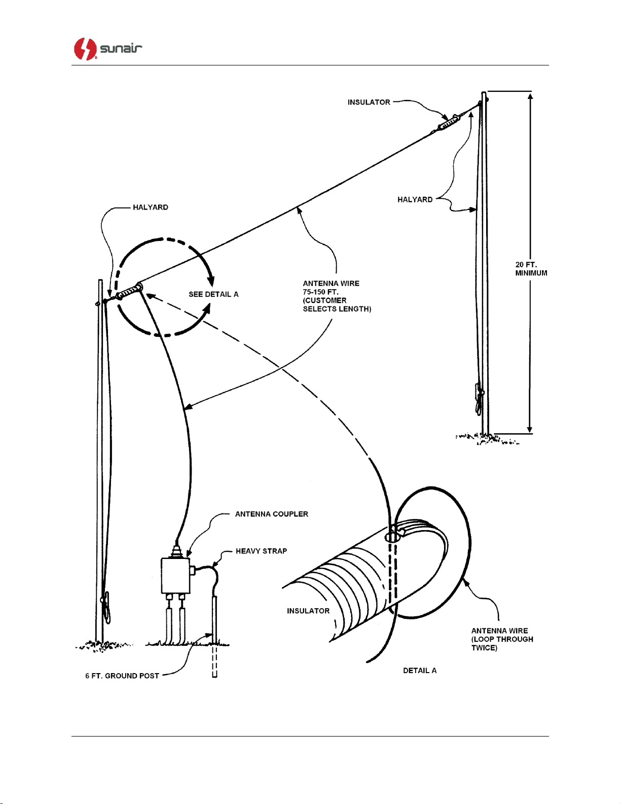
The longwire antenna, illustrated in Figure 2.11-5, is a popular base station antenna where a wide
range of operating frequencies are used. The antenna impedance varies greatly with frequency
and, therefore, must be matched to the transmitter with the antenna coupler. The CU-9150 will
efficiently match longwire antennas up to 150 foot in length. The radiation pattern of the
longwire antenna is also a strong function of operating frequency. The two most popular
longwire antennas, (75 and 150 foot) available from Sunair, exhibit excellent low frequency
radiation efficiency.
2.7 Long-Wire Adapter Kit (1A1A5) 8120909003
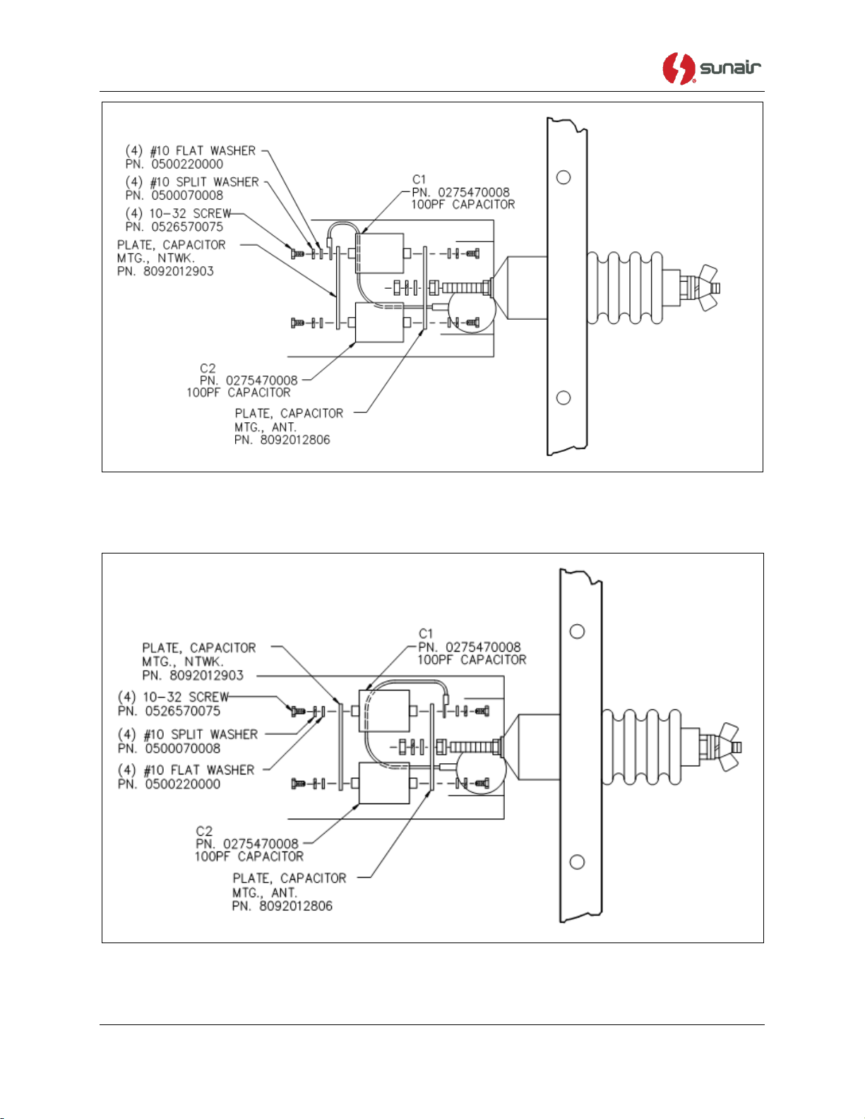
The Long-Wire Adapter Kit is required for wire antennas between 50 and 150 feet in length. See
Figure 2.11-6 for installation details.
Operation using a 23- to 35-foot whip antenna is still possible after installation of the long-wire
adapter kit. This is accomplished by changing the point at which the wire from K19 on the
chassis (1A1K19) is connected to the long-wire adapter kit. See Figure 2.11-7 for details.
A WHIP / LONG-WIRE identification plate is included with the long-wire adapter kit. It should
be secured to the top cover of the coupler by one of the cover hold-down screws. It is meant to
indicate whether the long-wire adapter kit is configured for whip or long-wire operation.
2-4 Use or disclosure of information from this document is subject to the restrictions
indicated on the proprietary/confidentiality page of this document.
Page 25

CU-9150
2.8 TX Only Function
If the coupler is being installed in a system with separate transmit and receive antennas and
where two or more transmitters are using collocated antennas, the TX ONLY function should be
enabled. When this function is enabled, the coupler opens the RF path between the tuning
network and the radio system when the radio system is in receive mode. Therefore, high RF
voltages induced by adjacent transmitters are confined to the coupler.
The TX ONLY function is enabled by soldering a jumper wire between E4 and E4 of the
1A1A4A1 RF Detector Board.
2.9 Software Revision
In order for the CU-9150 to function properly, the software revision in the companion
transceiver or exciter and linear amplifier must be equal to or later than the following:
Equipment Software Revision
RT-9000 or RT-9000A D4
T-9400 B1
LPA-9500 B1
LPA-9600 B1
2.10 Checks after Installation
Follow steps outlined in Section 3.2 for your particular system configuration.
WARNING - HIGH VOLTAGE
The radio operator and service technician should exercise caution not to
contact the ANTENNA INSULATOR E2 output while transmitting.
2.11 Integration with Third Party Radio Systems
Refer to Section 4.9 for interface information required to integrate the CU-9150 with Third Party
Radio Systems.
Use or disclosure of information from this document is subject to the restrictions 2-5
indicted on the proprietary/confidentiality page of this document.
Page 26

CU-9150
Figure 2.11-1. CU-9150 Control Cable P/N 8092500096
2-6 Use or disclosure of information from this document is subject to the restrictions
indicated on the proprietary/confidentiality page of this document.
Page 27

CU-9150
Figure 2.11-2. Coupler Outline Dimensions
Use or disclosure of information from this document is subject to the restrictions 2-7
indicted on the proprietary/confidentiality page of this document.
Page 28

CU-9150
THIS PAGE INTENTIONALLY LEFT BLANK
2-8 Use or disclosure of information from this document is subject to the restrictions
indicated on the proprietary/confidentiality page of this document.
Page 29

CU-9150
Figure 2.11-3. LPA-9600 with CU-9150, 35-Foot Antenna (Roof Top Installation)
Use or disclosure of information from this document is subject to the restrictions 2-9
indicted on the proprietary/confidentiality page of this document.
Page 30

CU-9150
Figure 2.11-4. LPA-9600 with CU-9150, Non-Resonant Antenna
2-10 Use or disclosure of information from this document is subject to the restrictions
indicated on the proprietary/confidentiality page of this document.
Page 31
CU-9150
Figure 2.11-5. Longwire Antenna Kit
Use or disclosure of information from this document is subject to the restrictions 2-11
indicted on the proprietary/confidentiality page of this document.
Page 32
CU-9150
Figure 2.11-6. Long-Wire Adapter Kit (1A1A5) 81200909003 Installation Configured for
Long-Wire Operation
Figure 2.11-7. Long-Wire Adapter Kit (1A1A5) 81200909003 Installation Configured for
Whip Wire Operation
2-12 Use or disclosure of information from this document is subject to the
restrictions indicated on the proprietary/confidentiality page of this document.
Page 33
CU-9150
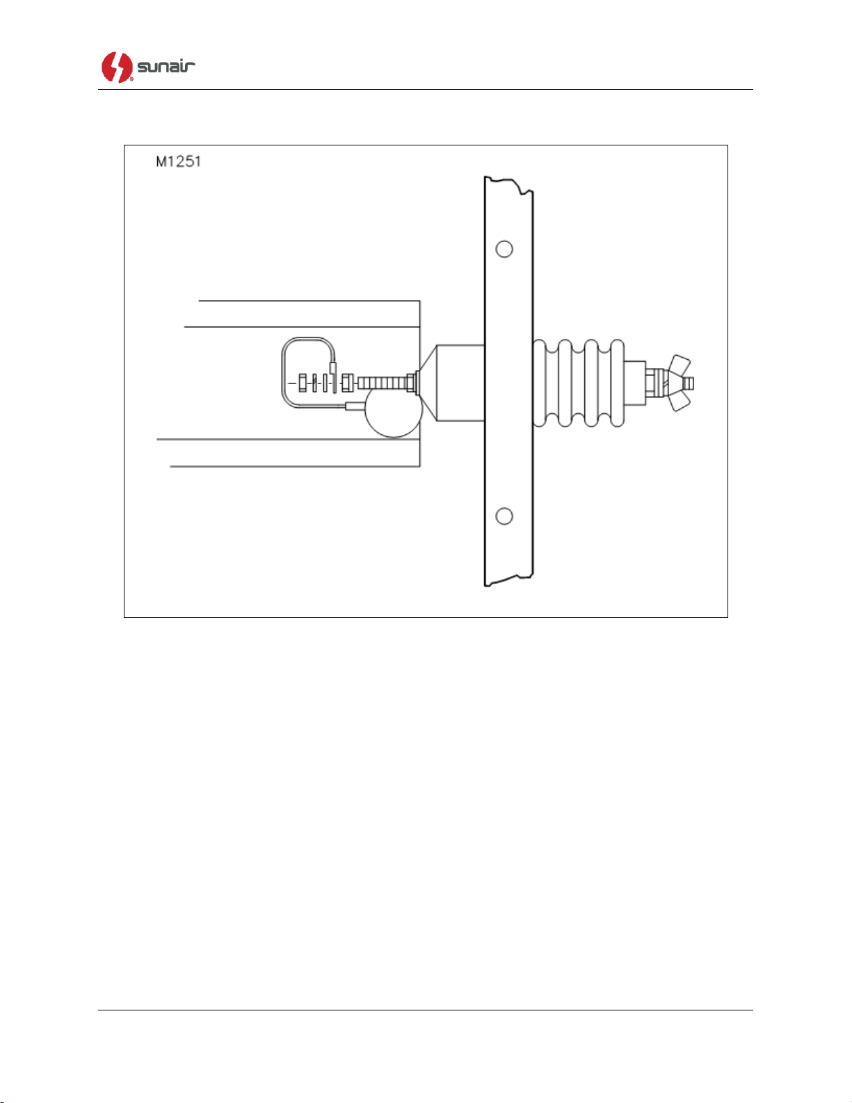
Figure 2.11-8. Assembly/Disassembly of Antenna Output Lead (Long-Wire Adapter Kit
Not Installed)
END OF CHAPTER II
Use or disclosure of information from this document is subject to the restrictions 2-13
indicted on the proprietary/confidentiality page of this document.
Page 34

CU-9150
THIS PAGE INTENTIONALLY LEFT BLANK
2-14 Use or disclosure of information from this document is subject to the
restrictions indicated on the proprietary/confidentiality page of this document.
Page 35

CU-9150
CHAPTER III – Operation
3.0 Operation
3.1 General
The CU-9150 Automatic Digital Antenna Coupler operates with the LPA-9600 1 kW or LPA9500 500 Watt Solid State Linear Power Amplifier and 9000 Series Exciters/Transceivers. Refer
to the LPA-9600 or LPA-9500 manual and/or the applicable Exciter/Transceiver manual for
operational considerations of the individual unit.
3.2 Operating the CU-9150
3.2.1 Operation with 9000 Series Exciters/Transceivers and LPA-9600
Ensure that the Exciter/Transceiver, LPA-9600/LPA-9500 and CU-9150 are installed properly.
Refer to Section II of the applicable manuals.
1. Apply power to the Exciter/Transceiver and LPA-9600 and select 1 kW (for the LPA-
9500, select 500 W).
2. On the LPA-9600/LPA-9500, the green POWER lamp will light and the LCD will
display system messages:
FAULT: COUPLER UNTUNED, METER: FWD, PWR LVL: 1 kW (LPA-9500
displays 500 W)
3. Select desired operating frequency on the Exciter/Transceiver.
4. Press the CPLR TUNE pushbutton on the Transceiver front panel.
5. On the LPA-9600/LPA-9500, the following system messages will appear:
COUPLER TUNING, COUPLER TUNED, KW SYSTEM OPERATIONAL
6. Tuning will be accomplished in typically 1 to 2 seconds.
7. lf the red FAULT lamp of the LPA-9600/LPA-9500 lights during a tune attempt, the CU-
9150 has not tuned. Press the CPLR TUNE pushbutton again and allow the system to
retune. If the FAULT does not clear, refer to Section 5.0 of this manual and the
Exciter/Transceiver manual.
3.2.2 1000 Watt Operational Checkout
1. Select CW MODE and frequency 29.9900 MHz. Press the CPLR TUNE pushbutton and
observe a SYSTEM READY condition.
2. Key the Exciter/Transceiver with the CW key and check the forward and reflected power
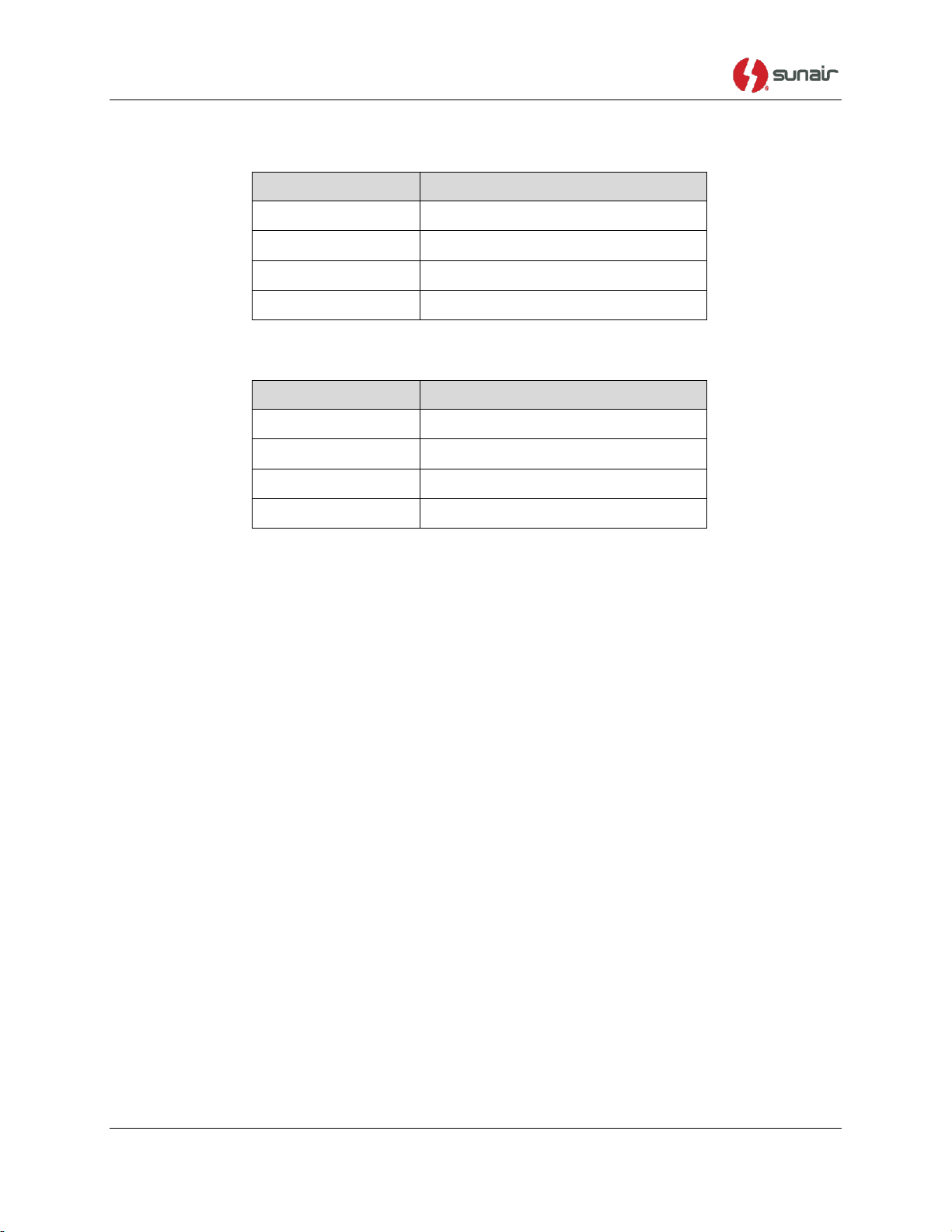
on LPA-9600 front panel meter. An acceptable tune should show 700 to 1000 Watts
forward and 28 to 40 Watts reflected maximum. Refer to Table 3.2-1.
NOTE The LPA-9500 should show 300 to 500 Watts (refer to Table
3.2-2).
Use or disclosure of information from this document is subject to the restrictions 3-1
indicated on the proprietary/confidentiality page of this document.
Page 36
CU-9150
Forward Watts
Reflected Watts Maximum
700
28
800
32
900
36
1000
40
Forward Watts
Reflected Watts Maximum
350
14
400
16
450
18
500
20
Table 3.2-1. Acceptable Reflected Power Chart for VSWR 1.5:1. for LPA-9600
Table 3.2-2. Acceptable Reflected Power Chart for VSWR 1.5:1. for LPA-9500
3. Continue tuning through the HF Spectrum from 1.6 to 30 MHz in 1 MHz steps and check
for an acceptable tune at each frequency. If problems occur, refer to Section to determine
how to correct the problem.
END OF CHAPTER III
3-2 Use or disclosure of information from this document is subject to the
restrictions indicated on the proprietary/confidentiality page of this document.
Page 37

CU-9150
CHAPTER IV Theory of Operation
4.0 Theory of Operation
4.1 General
The CU-9150 is a fully digital antenna coupler designed for use with the LPA-9600 1 kW or
LPA-9500 500 Watt Linear Power Amplifiers and the Sunair 9000 series Exciters and
Transceivers. The coupler is rated for 1000 Watts PEP or average power and will tune common
shipboard and ground based antenna systems such as 23 foot and 35 foot verticals or 50 to 150
foot end-fed wire antennas.
A 128 channel non-volatile memory system is provided for use with Transceivers or Exciters
providing channel information to the coupler.
Figure 4.9-2 provides an assembly tree of all the major assemblies, their part numbers, and
reference designations. Figure 4.9-3 provides a block diagram for the unit. Both are at the end of
this section.
4.2 Antenna Impedance Matching Network
The antenna impedance matching network is a lowpass PI and PI-L network depending on the
frequency and antenna system employed. The lowpass PI network offers several desirable
advantages over high-pass network configurations such as:
Harmonic Attenuation. 5 to 20 dB depending on the antenna type and operating
frequency.
Pipeline Operation (Bypass) for Automatic Link Establishment (ALE) receives scan
operation. This technique conserves mechanical relay life.
The PI network can be viewed as two L-networks placed in back-to-back configuration. The PI
network is very flexible, it can provide a number of network component solutions for any one
impedance matching problem, by modifying the antenna impedance with shunt output
capacitance. However, excessive amounts of shunt output capacitance results in a low network
impedance, producing significant circulating current in both the series-L and shunt C
components. The CU-9150's RF network and tuning algorithm have been carefully designed to
use the minimum amount of output capacitance required to achieve a satisfactory network
solution. This ensures that the matching network operates at maximum efficiency and reduces
electrical stress on the RF network components and relays.
Operation at 5 MHz and above with the specified antennas results in a PI-network solution.
When operating below 5 MHz, with electrically short antennas, a large negative reactive
component will appear at the antenna terminal. To solve this, additional series inductance is
required: three selectable values are included in the network, transforming it to a PI-L.
Frequency information is supplied to the coupler via the channel lines.
A block diagram of the CU-9150 is shown in Figure 4.9-3. The input capacitor bank (50 Ohm
side), located on the Input Capacitor Assembly, consists of C1 through C11D and provides
binary stepped capacitance values from 5.6 pF to 10,233 pF. The L series inductor assembly
consists of inductors L1 through L9 providing binary stepped inductance values of 0.025 µH
Use or disclosure of information from this document is subject to the restrictions 4-1
indicated on the proprietary/confidentiality page of this document.
Page 38

CU-9150
through 12.75 µH. The L-out assembly consists of L10 through L12, providing 12.6 µH through
63 µH. The output capacitor bank, consisting of C2 through C6D provides binary stepped
capacitance values from 25 pF to 775 pF. Capacitor C1, 15 pF serves as a fixed ballast capacitor.
4.3 Chassis Assembly 1A1
4.3.1 General
The chassis assembly contains the RF network components, Input Connector Assembly 1A1A2,
CPU Assembly 1A1A3, RF Detector 1A1A4A1, Input Capacitor Assembly 1A1A4A2 and
Mother Board Assembly 1A1A1.
4.4 Input Connector Assembly 1A1A2
4.4.1 General
The Input Connector Assembly serves as the interconnect between the LPA-9600/9500 and 9000
series radio equipment.
4.4.2 Configuration and Operation
The Input Connector Assembly provides T-lowpass RF filters on each of the signal, control and
power lines entering and exiting the CU-9150 with the exception of the TX/RX data lines. The
TX/RX data lines are used during service or system evaluation and are normally not connected
during routine operation. The T-lowpass filters prevent unwanted RF radiation emitted by the
antenna matching network from appearing on the control cable and interfering with the
companion transceiver or exciter circuitry.
In addition to this protection, each of the aforementioned lines are supplied with Metal Oxide
Varistor, transient voltage surge suppressors. The suppressors will minimize transient voltage
levels that can appear on any signal, power or control line in the event of a lightning surge.
4.5 CPU Assembly 1A1A3
4.5.1 General
The CPU Assembly contains the system microprocessor, memory, D/A converter and relay
drivers.
4.5.2 Microprocessor
The CPU assembly utilizes the 80C188EB (16 bit internal / 8 bit external) microprocessor, U103,
operating at an external clock speed of 14.7456 MHz. The 80C188EB contains internal chip
select logic, three hardware timers, parallel I/O, and two asynchronous serial I/O channels in
single package. Its operating firmware is contained in EPROM (27C010-040), U301. SRAM
(TC551001), U302 is used to hold program variables and temporary data such as phase and
magnitude discriminator error correction levels. EEPROM (28C64-256), U303 is non-volatile
memory used to store channel network solutions.
The 80C188EB controls its associated memory and peripherals using three busses:
4-2 Use or disclosure of information from this document is subject to the restrictions
indicated on the proprietary/confidentiality page of this document.
Page 39

CU-9150
AD0 through AD7, a multiplexed address/data bus containing either data or address
information.
A8 through A15, which always contain address information.
The Control/Status bus, which contains signals RD, WR, IO/M, and ALE.
4.5.3 Serial Communication
Communication between the microprocessor and the Serial Breakout Board on the TS-9150
Diagnostic Test Set is mainly accomplished by U101. U101 is a MAX490 RS-422 interface
chip. Since R111 and R112 are installed and L101 and L102 are not installed, the system is
configured for transmitting RS-422 data only. This data is sent over the control cable to the
Serial Breakout Board, where it is converted to RS-232 levels. After conversion, the data is sent
to a PC for display.
4.5.4 A/D Converter
U208 is an LTC1290 12 bit analog to digital converter. It reads the analog voltages from the RF
Detector board and converts them to a digital serial stream which can be read by the
microprocessor. The output values from the LTC1290 are accurate to within 1.25 millivolts.
4.5.5 Relay Drivers
Several different types of relay drivers are used on the CPU board. The first type is the
UCN5801A (U401-403). These drivers supply coil current to the relays on the Input Capacitor
board. U401, U402, and U403 are addressed over the parallel data bus of the microprocessor.
The second type of relay driver is a UCN5842A (U501-U504 and U304). These drivers are
loaded serially by the microprocessor. U501 through U504 are used to drive the K44P type
relays on the coupler chassis. The K44P relays are used to switch the Lseries and Cout network
components. U304 lights the status LEDs and sends the READY and FAULT signals back to
the radio. U304 also drives the tune/bypass relays on the RF Detector board (1A1A4A1K1 and
1A1A4A1K2), and the soft start relay on the motherboard (1A1A1K101).
The last relay driver type consists of U404, U405, and Q401-Q404. U404 is addressed over the
parallel data bus. U405 converts the 5 volt output of U404 to 12 volt logic which drives Q401
through Q404. These transistors provide the coil current for the KC-12 relays on the coupler
chassis. The KC-12 relays are used to switch the Lout network components.
4.5.6 Channel Change and Tune Command Detectors
In normal operation, the 80C188EB microprocessor is only active when tuning or changing
channels. The rest of the time, the microprocessor is in “Powerdown Mode”. In Powerdown
Mode, the microprocessor oscillator is stopped. This prevents the oscillator from being heard by
the radio receiver.
When the microprocessor is in Powerdown Mode it can only be started up by a RESET signal or
a non-maskable interrupt (NMI). Therefore the CPU assembly includes circuitry to detect when
the channel information from the radio has changed. When the channel does change, an NMI
signal is generated.
Use or disclosure of information from this document is subject to the restrictions 4-3
indicated on the proprietary/confidentiality page of this document.
Page 40

CU-9150
The channel change detector consists of U604, U605, and U601. The microprocessor reads the
channel lines through U605. Every time a read is performed, the state of each channel line is
latched by U604. U605 compares the current channel state from the radio with the state stored in
U604. If they are different, a CHANNEL CHANGE signal is sent to U105. U105 generates an
NMI signal to “wake up” the microprocessor when it receives this CHANNEL CHANGE signal
or when a tune command is detected through U104.
4.6 RF Detector Assembly 1A1A4A1
4.6.1 General
The RF 1A1A4A1 Detector contains the phase and magnitude discriminators, -3 dB power pad
and precision 50 Ohm calibration termination resistor.
The RF detector provides two variable dc signal voltages to the CPU. The phase signal voltage is
proportional to the reactive component of the impedance and the magnitude signal voltage is
proportional to the magnitude of the impedance. The phase and magnitude signals are referenced
to 50 Ohms.
4.6.2 Magnitude Discriminator
The magnitude discriminator consists of RF transformer T2 and its associated components. It
provides a means of measuring the relative magnitude of the transformed antenna impedance
relative to 50 Ohms. For a impedance magnitude greater than 50 ohms, the magnitude
discriminator produces an output voltage less than the +2.5 VDC reference voltage. For a
magnitude less than 50 Ohms, an output greater than the +2.5 VDC reference voltage is
produced. A voltage sample is provided from the transmission line by C8 and C9 and is rectified
by CR9 producing a DC voltage proportional to the RF voltage on the line. A voltage
proportional to the current in the transmission line is generated by transformer T2 and is rectified
by CR7. Capacitor C8 is adjusted so that the voltage sample is exactly equal to the current
sample when the transmission line is terminated with 50 Ohm non-reactive load. The output of
this discriminator is supplied to A/D converter on the CPU assembly.
4.6.3 Phase Discriminator
The phase discriminator consists of transformer T1 and associated components. It provides a
means of measuring the relative phase angle at the input to the tuning network by comparing the
phase of the line voltage with line current. The phase discriminator output is zero when the
transmission line voltage and the current samples are in phase (pure resistance terminating the
transmission line). The voltage sample is delivered by C5 R9 and C6 which shifts the phase by
90 degrees. The current sample is generated by transformer T1 and is in phase with the line
current. The voltage sample is fed to T1 center tap and the resulting output is detected by CR4
and CR5, producing a DC voltage proportional to the phase difference between the voltage on
the transmission line and the current in the line. R8 is the phase discriminator balance control
and is adjusted so the phase output is nulled (relative to +2.5 V DC) when the transmission line
is terminated with a 50 ohm non-reactive load.
The output of this discriminator is supplied to A/D converter on the CPU assembly.
4-4 Use or disclosure of information from this document is subject to the restrictions
indicated on the proprietary/confidentiality page of this document.
Page 41

CU-9150
4.6.4 Attenuator Pad, -3 dB
The 3 dB PI-attenuator pad consists of precision power resistors R1, R2, R3 and R4. The pad is
switched between the antenna tuning network and the transmitter whenever the tune relays K1
and K2 are energized. The pad provides protection for the transmitter by limiting the impedance
variations placed on the transmitter during the tuning cycle. When a satisfactory tune has been
achieved, the pad is switched out. During normal operation (no tune cycle) the pad is not used.
Tune relays K1/ K2 and CR10 (Amber LED) are energized by the tune relay signal from the
CPU Assembly.
4.6.5 50 Ohm Calibration Termination
A 50 Ohm, 1% calibration termination resistor controlled by relay K3 allows the phase and
magnitude detectors to be calibrated at the beginning of the tune cycle.
When the tune command is received from the transceiver the CPU assembly engages the -3 dB
RF power pad and the calibration termination resistor. The phase and magnitude detectors are
then evaluated at the tune frequency and their respective error voltages are temporally stored in
the CPU memory. The calibration termination is then switched out-of-circuit and the detectors
are applied to the tuning network. During the tune cycle the phase and magnitude detector
voltage is compared with the 50 Ohm calibration voltage values stored in the CPU memory. The
RF tuning network solution is adjusted by the CPU to arrive at the 50 Ohm calibration voltage
levels.
This system provides two significant advantages over conventional RF detector systems:
The phase and magnitude detectors are calibrated for temperature and component
drift each time the coupler is tuned.
The phase and magnitude detectors do not require periodic field alignment.
4.6.6 TX Only Function
The TX Only function is used under the following conditions:
Separate transmit and receive antennas.
Two or more transmitters with collocated antennas. Typical of shipboard systems.
The TX Only function opens the RF transmission line between the RF network and the RF
input connector J1. This occurs only when the TX ONLY jumper E3 to E4 is installed and the
transceiver is in the receive condition or the exciter is in the standby condition. The open
transmission line prohibits high voltage generated from the adjacent transmitter from appearing
at peripheral equipment such as Pre-postselectors.
During tuning or transmitting the KEYLINE is low (less than 12 V DC). Comparator U1-A
buffers the low and turns Q2 off.
During receive the KEYLINE is high (greater than 12 V DC). Comparator U1-A buffers the
high, turning Q2 on. Q2 energizes relay K1. The common contact of K1 is connected to the
normally open and the common contact of K2 is connected the normally closed contact of K2,
thus opening the RF path to the RF IN terminal J1.
Use or disclosure of information from this document is subject to the restrictions 4-5
indicated on the proprietary/confidentiality page of this document.
Page 42

CU-9150
4.7 Input Capacitor Assembly 1A1A4A2
4.7.1 General
The Input Capacitor assembly is located on the 50 Ohm side of the RF tuning network.
4.7.2 Configuration and Operation
The Input Capacitor Assembly 1A1A4A2, consists of eleven binary capacitance values from 5.6
pF to 10,233 pF in 5.6 pF steps. Each binary capacitance value is constructed from porcelain
high RF power multilayer capacitors. These capacitors are specifically characterized for RF
transmitting duty and are ideally suited for antenna matching network application. Each of the
individual capacitance values are controlled by a single or dual magnetic latching relay. The
latching relays operate by placing a 10 ms pulse on the OPEN or CLOSE field winding.
Maximum operating time is 5 ms. Relay drivers and their control is provided by the CPU
Assembly.
4.8 Mother Board Assembly 1A1A1
4.8.1 General
The Mother Board 1A1A1 interconnects all assemblies, including the RF network relays,
through printed circuit wiring tracks, with exception of the Input Connector Assembly which is
connected to the Mother Board by ribbon cable.
4.8.2 DC Power
+28 Volt DC power, supplied by the transceiver or exciter, is filtered by capacitors C1 and C2. A
total of 13,600 µF is provided. During power-up the capacitors are charged through a 3 Ohm
resistor, R1. When the CPU +5 VDC power is achieved and the microprocessor is operating
correctly, the microprocessor energizes K101, bypassing resistor R1.
4.8.3 Series L and Shunt C Relays
The series L, K1-9 and Shunt C, K10-14, relays utilize latching high-speed RF relays that switch
the inductive series and capacitive shunt network elements. The relays operate by placing a 7 ms
pulse on the OPEN or CLOSE field winding. Maximum operating time is 5 ms.
Each relay is rated for 7 kV and 35 amperes at 2.5 MHz. These ratings, of course decrease as the
operating frequency increases, but in all expected network configurations, the relays are
conservatively rated.
4.8.4 L-OUT Relays
The L-Out relays, K16, 17 and 18, control the high-value series inductors. These relays and
associated network components are used with electrically short antennas such as 23 or 35 foot
whip antennas and operating frequencies below 3 MHz. At 1000 Watts, extremely high voltages
and high currents can be expected in the L-Out network. This places special operating
requirements on these relays. Each relay is rated for 15 kV and 30 amperes at 2.5 MHz. In all
expected network configurations, the relays are conservatively rated.
4-6 Use or disclosure of information from this document is subject to the restrictions
indicated on the proprietary/confidentiality page of this document.
Page 43
CU-9150
Signal
Description
TUNE
COMMAND
This signal is used to initiate a coupler tune. A low is 0V to 2.5V and a
high is 7.5V to 12V. A high on this line indicates that the radio system is
requesting a tune cycle. The coupler will respond by bringing +28V TUNE
ENABLE high (to 28V). The radio system should then bring TUNE
COMMAND low and wait for the coupler to bring +28V TUNE ENABLE
low. At this point the coupler is ready to receive frequency information
over the channel lines. The radio system should then output the
frequency in megahertz, in packed BCD format, on the channel lines.
Bringing TUNE COMMAND high will cause the coupler to latch the
frequency information. When the coupler brings +28V TUNE ENABLE
high for the second time, it indicates that the frequency information has
been read and that the radio should restore the channel to the channel
lines. See Figure 4.9-1 for details of this operation and timing
requirements. TUNE COMMAND should be brought low before the
application of tune power.
+28V TUNE
ENABLE
This is a PNP open collector output. Maximum output drive is 15 mA.
Maximum output voltage is the voltage at the +28V supply input. See
TUNE COMMAND for details regarding the meaning of this output.
READY
This active low output is pulled low when the coupler is in a tuned state
and can accept 1KW RF power. This is an open collector output. At a
sink current of 100 mA, the output voltage will be less than 1.1 V. This
output is rated for 50 V in the off state. When READY is pulled low,
indicating the end of a successful tune, the radio system should stop
transmitting tune power. When the coupler detects that tune power has
been removed, it will bring +28V TUNE ENABLE low. At this point the
coupler is ready to operate at the 1KW power level.
FAULT
This active low output is pulled low when the coupler has failed to find a
network solution. This is an open collector output. At a sink current of
100 mA, the output voltage will be less than 1.1 V. This output is rated
for 50 V in the off state. When FAULT is pulled low, indicating the end of
a failed tune, the radio system should stop transmitting tune power.
When the coupler detects that tune power has been removed, it will bring
+28V TUNE ENABLE low.
KEYLINE
This signal is presently unsupported by the coupler and should be left
unconnected.
The L-Out relays are conventional non-latching relays and must have continuous field current to
operate.
4.9 Interface Requirements for Third Party Equipment
4.9.1 Signal Descriptions
Table 4.9-1 provide a description of signals.
Table 4.9-1. Signal List and Descriptions
Use or disclosure of information from this document is subject to the restrictions 4-7
indicated on the proprietary/confidentiality page of this document.
Page 44

CU-9150
Signal
Description
Channel Lines
These 8 channel lines are used to provide the coupler with channel and
frequency information. A 10K pull-down resistor is provided which pulls
each line to ground. Each line should be pulled to between 3.5V and 5.0V
to assert a high. Channels 0 thru 127 are valid for normal operation.
These lines are active low, so to select channel 0 (for example) all lines
must be pulled to 5V. These lines are also active low when passing
frequency information in packed BCD (Binary Coded Decimal) format, so
to select 15 MHz (for example), 0xEB must be driven on the channel
lines.
COUPLER
DETECT
This line allows the radio system to detect the presence or absence of a
coupler. This signal is high (about 21 V) when a coupler is present.
Current draw from this line should be less than 30mA.
+28V
This is the power supply for the coupler. This supply must be between
22V and 30V. Maximum inrush current is limited to 10A by the 3 ohm
resistor R1 on the motherboard. Maximum idle current is 2A. Maximum
current draw during a tune cycle is 5A.
RF INPUT
Maximum RF input power when READY is low is 1KW PEP. Tune power
should be between 25W and 75W.
Table 4.9-1. Signal List and Descriptions (Continued)
4-8 Use or disclosure of information from this document is subject to the restrictions
indicated on the proprietary/confidentiality page of this document.
Page 45
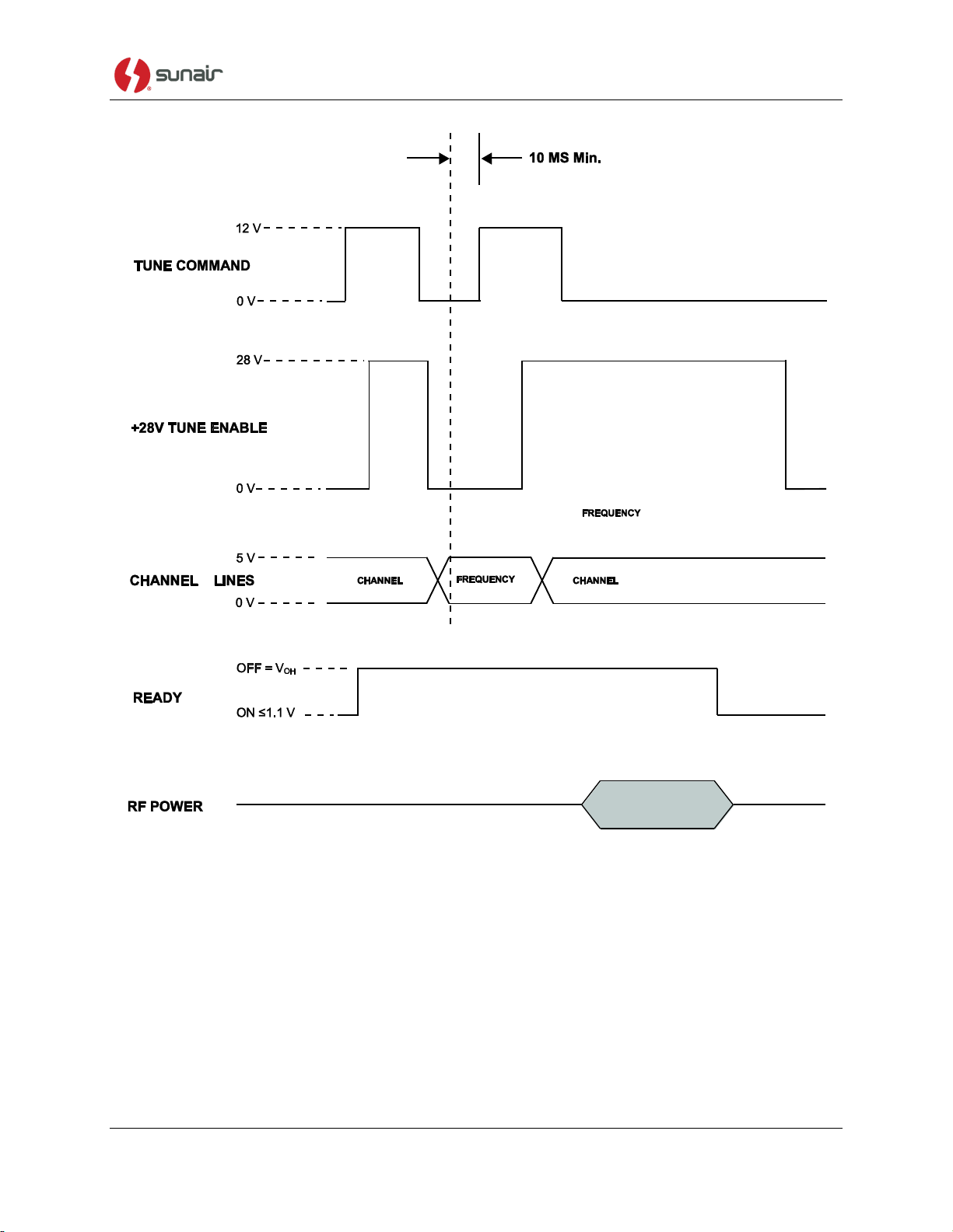
CU-9150
Figure 4.9-1. Coupler Interface Timing
Use or disclosure of information from this document is subject to the restrictions 4-9
indicated on the proprietary/confidentiality page of this document.
Page 46
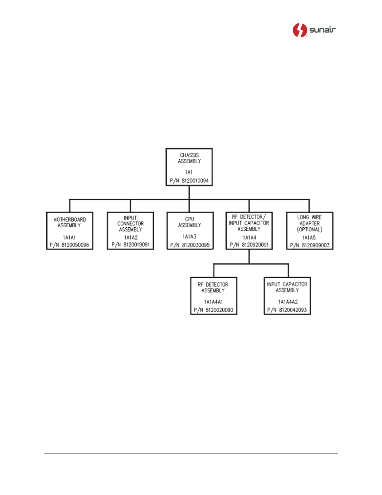
CU-9150
Figure 4.9-2. CU-9150 Assembly Tree
4-10 Use or disclosure of information from this document is subject to the restrictions
indicated on the proprietary/confidentiality page of this document.
Page 47
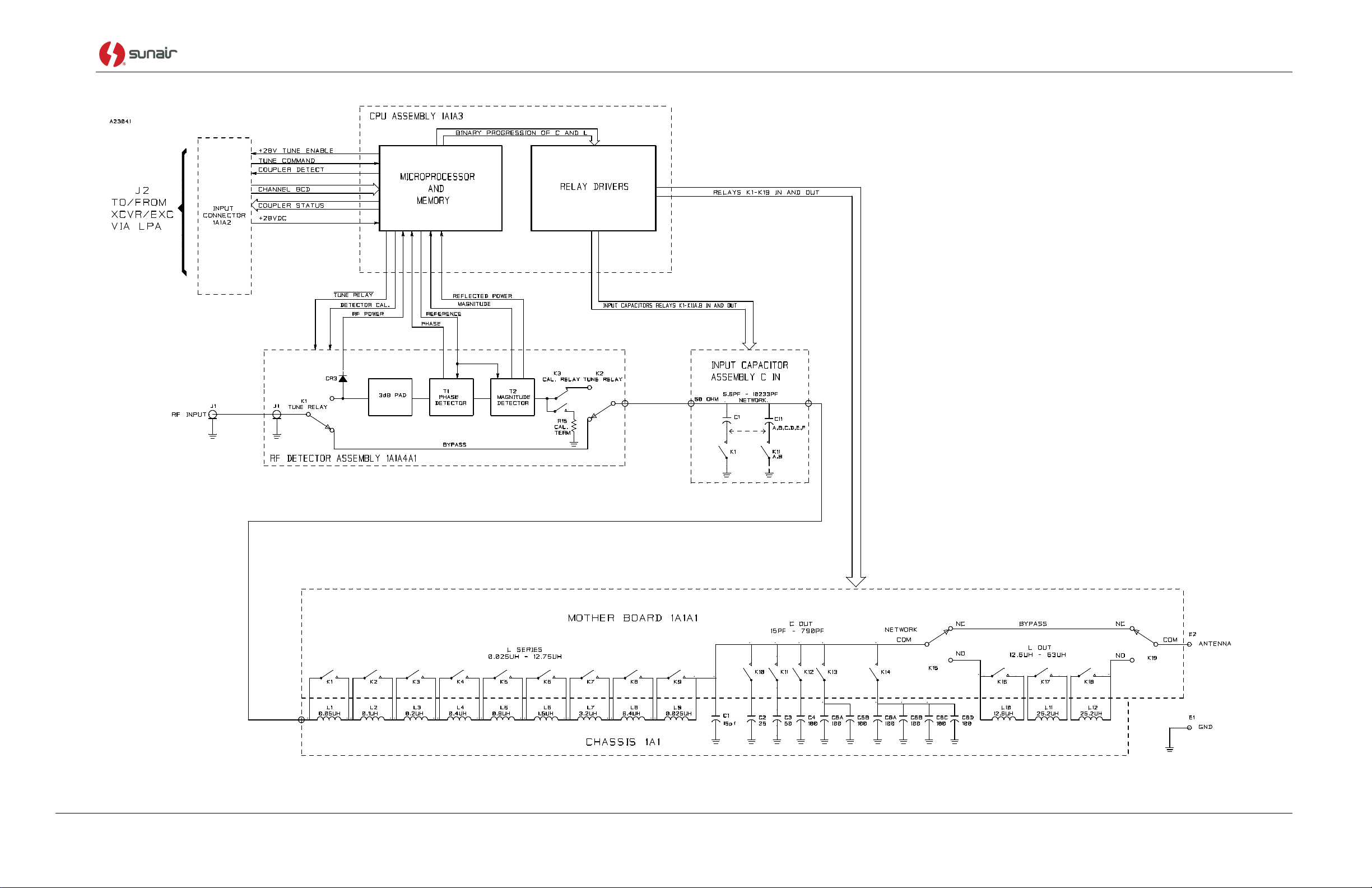
CPU-9150
Figure 4.9-3. CU-9150 Block Diagram
Use or disclosure of information from this document is subject to the restrictions 4-11
indicated on the proprietary/confidentiality page of this document.
Page 48

CU-9150
THIS PAGE INTENTIONALLY LEFT BLANK
4-12 Use or disclosure of information from this document is subject to the restrictions
indicated on the proprietary/confidentiality page of this document.
Page 49

CU-9150
Chapter V – Maintenance and Repair
5.0 General
This section provides the procedures for preventative maintenance, fault isolation, maintenance
and repair to the Lowest Repairable Unit (LRU) level.
5.1 Preventive Maintenance
Scheduled preventative maintenance ensures reliable operation of the CU-9150 antenna coupler.
Interval: Two (2) Weeks
When installed in a harsh maritime or tropical environment (i.e. salt air, salt water) wash the
complete outside of the coupler with fresh water.
Interval: Monthly
Inspect the unit for dust, dirt and foreign substance accumulation on the output insulator.
Also inspect for loose electrical connections, missing hardware, case deformation,
damaged fasteners or damaged electrical connectors.
Clean, adjust or replace as applicable.
Interval: Once a year.
Replace the gasket as described in Section 5.1.1.
With the top cover removed inspect the following:
1. Inspect connectors for broken parts, check insulation for cracks and check connector
pins for damage misalignment or bad plating
2. Inspect chassis wiring and subassemblies for any signs of physical damage or
charring. Any damaged wires must be replaced.
3. Inspect for leaky, blistered, charred or cracked electronic or electrical components.
Check for loose or corroded terminal connections.
5.1.1 Gasket Replacement
Whenever the coupler is opened the gaskets should be carefully inspected to ensure that they are
not cracked, broken, frayed or worn. If the gaskets require replacement, use the materials listed
below and complete the following procedure. See Figure 5.2-1.
5.1.1.1 Materials Required
The chemicals and gaskets specified in the procedure are available from Sunair.
8120001265: Gasket, Flat, Weldment, Case. Quantity 1 required per coupler.
1006990038: Cord, O-ring, .210 Diameter. Neoprene. Specify 8.0 feet per coupler when
ordering.
0864820003: GC Bond Cement, 2 fl. oz. (59 ML).
Use or disclosure of information from this document is subject to the restrictions 5-1
indicated on the proprietary/confidentiality page of this document.
Page 50

CU-9150
0840330006: Super Glue, 0.07 oz. (2 Grams).
1013140001: Super Lube Corrosion Inhibitor, 3.0 oz. (85 Grams).
5.1.1.2 Replacement Procedure
1. Remove and discard the flat and O-ring gaskets.
2. Clean the case gasket mounting surface and the O-ring gasket mounting grove on the top
cover.
3. Install the self-adhesive flat gasket P/N: 8120001265. Ensure that the holes in the gasket
align with the holes in the case.
4. Cement the O-ring gasket P/N: 1006990038 into the top cover groove using GC
Electronics GC Bond cement, GC Electronics P/N: 10-4302 or equivalent at
approximately three spots along each of the 4 sides.
5. Join the O-ring ends and trim the excess material with a razor.
6. Apply a small amount of Ross Super Glue or equivalent where the ends meet.
7. Apply a small amount of Super Lube Corrosion Inhibitor, Permatex (Loctite) P/N: 82325
or equivalent to each of the 18 top cover 10-32 x 1" mounting screws.
8. Install the top cover using the 10-32x1" mounting screws, lock and flat washers. Hand
tighten the mounting screws.
9. Tighten the screws using a torque screwdriver adjusted for 15 inch-pounds. Follow the
torque sequence procedure described in Figure 5.2-1.
5.2 Disassembly
Disassembly should be only to the extent necessary to accomplish the repair or replacement of
the defective LRU.
5.2.1 Cover Removal
Three covers are present in the CU-9150. For most maintenance procedures, all three covers
must be removed.
1. The top cover is taken off by removing the 18 Phillips head screws around the perimeter.
2. The clear plastic safety shield is removed by unscrewing four Phillips head screws.
3. The inner cover is removed by unscrewing four Phillips head screws.
5.2.2 CPU Removal
The CPU Assembly (1A1A3) is removed by grasping it firmly at the top of the assembly and
pulling straight up.
5-2 Use or disclosure of information from this document is subject to the restrictions
indicated on the proprietary/confidentiality page of this document.
Page 51
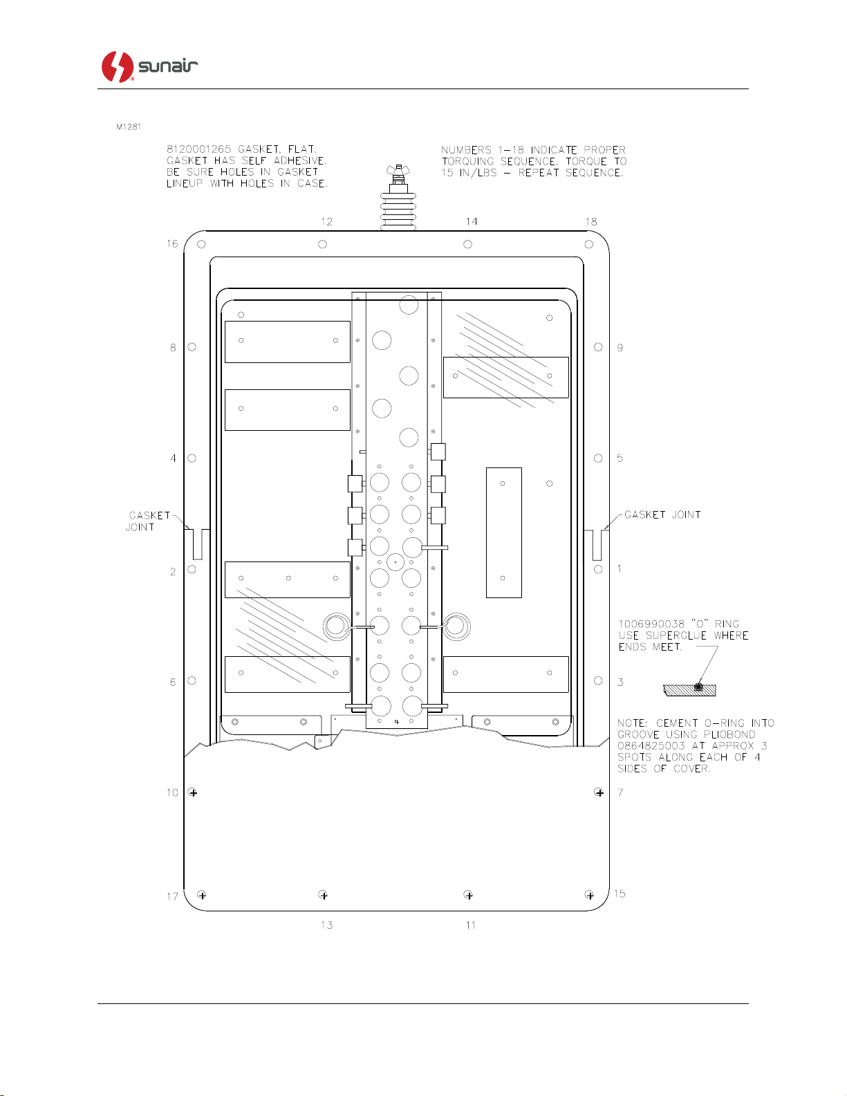
CU-9150
Figure 5.2-1. Gasket Installation and Torque Sequence
Use or disclosure of information from this document is subject to the restrictions 5-3
indicated on the proprietary/confidentiality page of this document.
Page 52

CU-9150
5.2.3 RF Detector/Input Capacitor Removal
Before removing the RF Detector/Input Capacitor Assembly (1A1A4), disconnect the coaxial
cable going to the RF Detector (1A1A4A1J1) and remove the screw connecting the Input
Capacitor Board (1A1A4A2) to the RF Network on the 1A1 Chassis Assembly.
CAUTION Failure to remove the screw connecting the 1A1A4A2
input capacitor board to the RF network on the 1A1
chassis will result in damage to the input capacitor board
as the assembly is removed.
Remove the RF Detector/Input Capacitor Assembly by grasping it firmly at the top of the
assembly and pulling straight up.
5.2.4 Chassis Removal
Before removing the Chassis Assembly (1A1) from the case, remove the retaining clip from the
ribbon cable going from the Motherboard (1A1A1) to the Input Connector Board (1A1A2J2) and
disconnect the cable. Also disconnect the coaxial cable going to the RF Detector (1A1A4A1J1).
If the 1A1A5 Long Wire Adapter Kit is installed:
1. Remove the lead going from K19 on the chassis to the Long Wire Adapter Kit (see
Figure 2.11-6 for details).
2. Using a 7/16” nutdriver, remove the nut holding the Long Wire Adapter to the
antenna output insulator and remove the Long Wire Adapter.
If the 1A1A5 Long Wire Adapter Kit is not installed:
1. Remove the lead going from K19 on the chassis to the antenna output insulator.
2. Using a 7/16” nutdriver, remove the seven nuts holding the chassis to the bottom of
the case. Remove the seven split washers. See Figure 5.2-2.
CAUTION When removing the Chassis Assembly, grasp it only by
the sheet metal components or by the white standoffs
that support the clear plastic safety cover. Do not grasp
the inductors, capacitors, relays, straps, or wiring.
Remove the chassis from the case in the following manner:
1. Lift the chassis straight up about 1/2” to clear the studs in the case.
2. Lift the CPU side of the chassis high enough to clear the side of the case and slide the
chassis out in that direction.
5-4 Use or disclosure of information from this document is subject to the restrictions
indicated on the proprietary/confidentiality page of this document.
Page 53
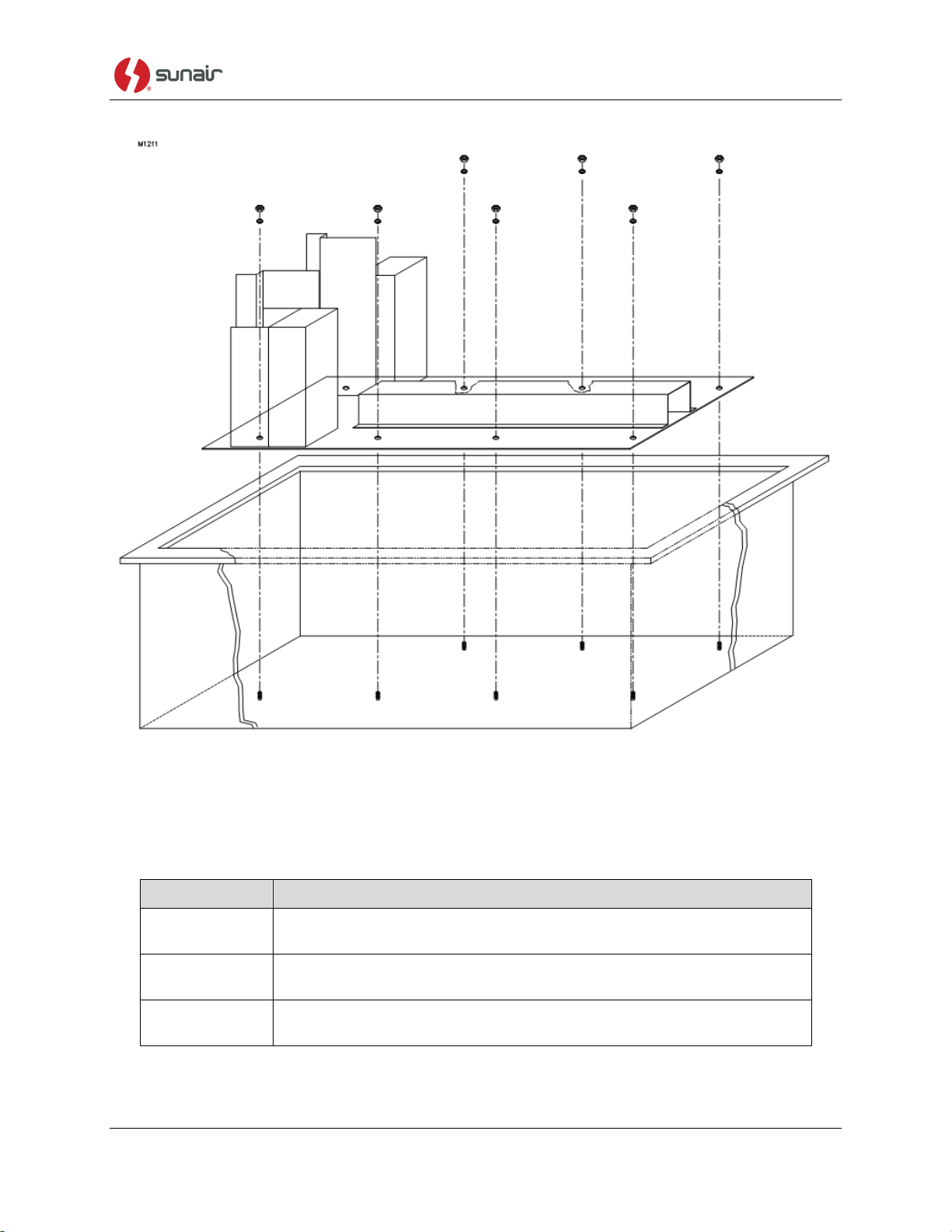
CU-9150
Indicator
Meaning
READY
This green LED on the 1A1A3 CPU (CR302) indicates that the coupler is
tuned and ready for RF from the radio system.
TUNING
This yellow LED on the 1A1A3 CPU (CR301) indicates that the coupler is
attempting to find a tune solution.
TUNING FAULT
This red LED on the 1A1A3 CPU (CR303) indicates that the coupler failed
to find an acceptable tune solution during the previous tune cycle.
Figure 5.2-2 Chassis Removal
5.3 Indicators
Table 5.3-1 lists the indicators and their meanings for the CU-9150.
Table 5.3-1. CU-9150 Indicators and Meanings
Use or disclosure of information from this document is subject to the restrictions 5-5
indicated on the proprietary/confidentiality page of this document.
Page 54

CU-9150
Indicator
Meaning
CPU FAULT
This red LED on the 1A1A3 CPU (CR304) indicates that a software error
occurred during the CPU program execution which prevents the program
from continuing. The CPU will stop program execution at the point where
the failure occurred, so the CPU must be reset, or the system power must
be cycled, to resume normal coupler operation.
TUNE RELAY
This yellow LED on the 1A1A4A1 RF Detector (CR10) indicates that the
magnitude discriminator, phase discriminator, and 3 dB pad are switched
into the RF path. This indicator is only lit when the TUNING indicator on
the CPU is lit.
Table 5.3-1. CU-9150 Indicators and Meanings (Continued)
5.4 Test Equipment Required or Equivalent
Digital Multimeter Fluke 77
Oscilloscope Tektronix 465
Alligator clip cables Two required
5.5 Alignment and Checks
Unless a component of the 1A1A4A1 RF Detector Assembly has failed and required
replacement, routine alignment of the CU-9150 is generally not required. This is due to the selfcalibrating nature of the CU-9150. At the beginning of each tune cycle, a 50-ohm calibration
load is switched in and the CPU reads the output of the magnitude and phase discriminators.
These readings are subtracted from all future measurements, ensuring that minor discriminator
imbalances over time, temperature, and frequency do not affect the network solution.
Alignment of the CU-9150 consists solely of adjusting a trimmer capacitor and a potentiometer
on the RF Detector Assembly (1A1A4A1). For component and test point locations see Figure
5.5-1. The alignment is accomplished as follows:
1. Turn off the radio set.
2. Remove the 1A1A3 CPU Assembly.
3. Connect the multimeter negative lead to ground on the RF Detector (1A1A4A1TP6).
Connect the positive lead to RF POWER (1A1A4A1TP1).
4. Using alligator clips, ground TP7 and TP8 on the 1A1A4A1 RF Detector to the chassis.
NOTE It may be necessary to remove the 1A1A4 RF Detector/Input Capacitor
Assembly in order to attach a test clip to TP8. Refer to Section 5.2.3 for removal
instructions for this assembly. If the assembly is removed, be certain to remove
the Phillips head screw which attaches the assembly to the 1A1 Chassis
Assembly.
5. Turn the radio set on (it is permissible to power up the coupler without the CPU installed
for alignment and troubleshooting). Set the frequency to 29.0 MHz. Set the mode to
5-6 Use or disclosure of information from this document is subject to the restrictions
indicated on the proprietary/confidentiality page of this document.
Page 55
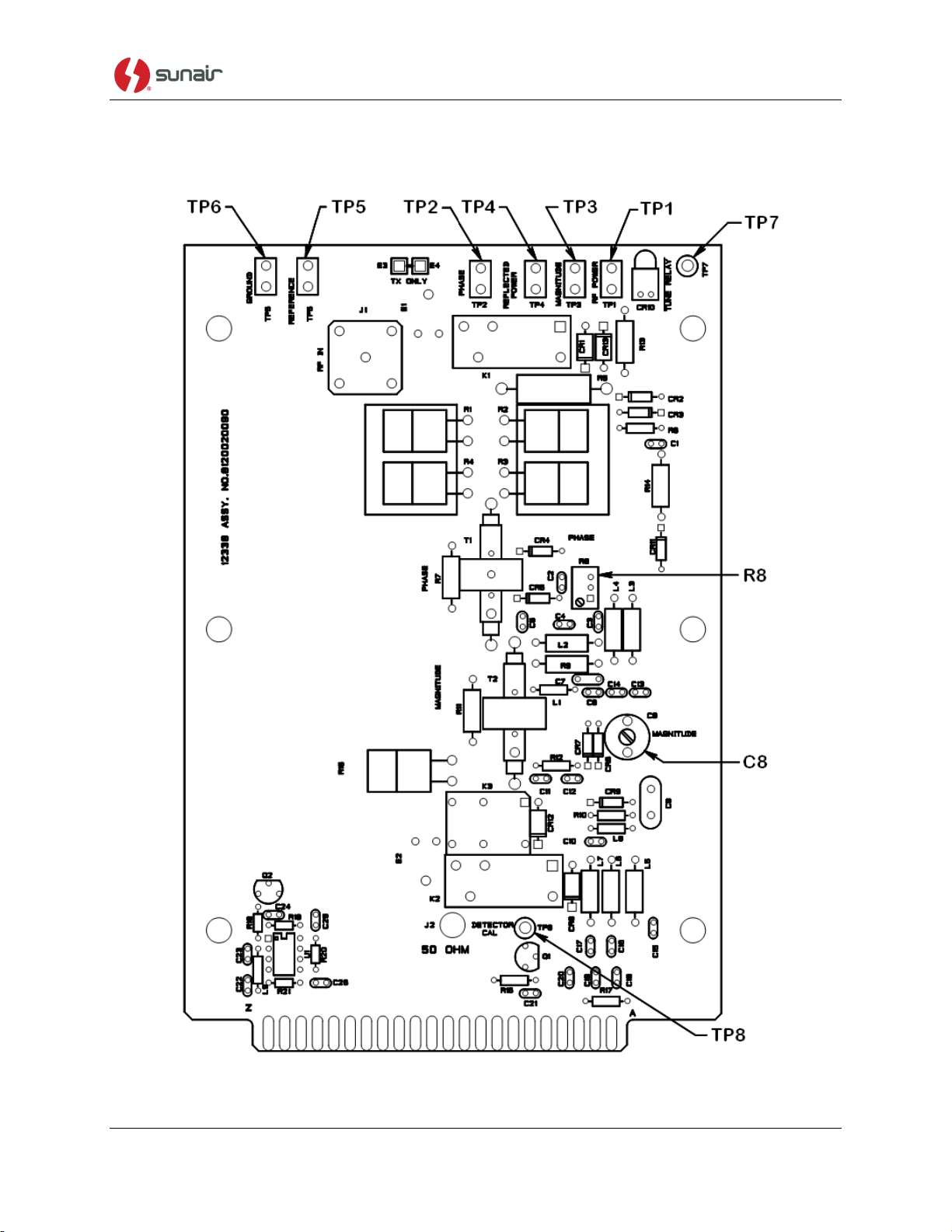
CU-9150
AM. Set the power level to 125W. If a linear amplifier such as a LPA-9600 or an LPA9500 is in the system, turn it off.
Figure 5.5-1. 1A1A4A1 RF Detector Alignment Adjustment Locations
Use or disclosure of information from this document is subject to the restrictions 5-7
indicated on the proprietary/confidentiality page of this document.
Page 56

CU-9150
CAUTION Applying more than tune power (AM carrier power in the 125w power
setting, which is about 40 watts) to the coupler during this alignment
procedure will destroy the pad and the calibration load on the RF detector
board.
6. Key the radio. The multimeter should read 4.0 to 5.5 volts DC.
7. Unkey the radio. Move the negative lead of the multimeter to the REFERENCE test
point (1A1A4A1TP5) and connect the positive lead to the REFLECTED POWER test
point (1A1A4A1TP4). Key the radio. The reading on the multimeter should not exceed
0.5 volts DC.
8. Unkey the radio. Move the positive lead of the multimeter to the PHASE test point
(1A1A4A1TP2). Key the radio. Adjust R8 on the RF Detector so that the reading on the
multimeter is between -.02 and .02 volts DC.
9. Unkey the radio. Move the positive lead of the multimeter to the MAGNITUDE test point
(1A1A4A1TP3). Key the radio. Adjust C8 on the RF Detector so the reading on the
multimeter is between -.02 and .02 volts DC.
10. Unkey the radio and turn it off. Remove the alligator clips and the multimeter. Put the
CPU back in the chassis.
5.6 Troubleshooting
5.6.1 Coupler Will Not Tune - No Relay Action - No Tuning Fault
1. Check for +28 volts DC at R1 on the 1A1A1 Motherboard Assembly. If the supply is not
present, check for +28 volts at L29 on the 1A1A2 Input Connector assembly. If +28
volts is not present at L29, the problem is probably due to the control cable between the
radio set and the CU-9150.
2. Check the voltage drop across R1 on the 1A1A1 Motherboard Assembly. A measured
drop greater than .1 volts indicates that the soft start relay K101 on the 1A1A1
Motherboard Assembly is not being engaged by the 1A1A3 CPU. This is generally the
result of the CPU not starting. Proceed to the next step for CPU troubleshooting.
3. Check for a green READY indicator on the 1A1A3 CPU after initial power-up. The lack
of a READY indicator indicates that the CPU is not executing its program correctly.
a. Check for +5V at U109 pin 20.
b. Check for +12V at U405 pin 16.
c. Check for a 14.7456 MHz signal with an amplitude of at least 4 volts peak to peak on
both sides of Y101.
d. If the three checks above look good, the CPU needs to be analyzed in its test fixture.
Refer to Section 6.1.2.1.
5-8 Use or disclosure of information from this document is subject to the restrictions
indicated on the proprietary/confidentiality page of this document.
Page 57

CU-9150
5.6.2 Coupler Will Not Tune - No Relay Action - Tuning Fault Indicated
Note the amount of time that elapses between pressing the CPLR TUNE button on the radio and
the coupler TUNING FAULT indicator lighting.
If this time is 10 seconds:
1. Using the oscilloscope, check for at least 20 volts peak to peak of RF at the RF INPUT to
the coupler during the tune cycle. If RF is not present at the input to the coupler, a
cabling problem probably exists between the radio set and the coupler.
2. If RF is present at the coupler input, check for the same signal at E1 of the 1A1A4A1 RF
Detector Assembly. If the RF signal did not make it this far, the cable between the RF
input and the RF Detector Assembly is probably bad.
3. Use the multimeter to check for 4.0 to 5.5 volts between TP1 (RF POWER) and TP6
(GROUND) during the tune cycle. The CPU waits for this signal to go high before
starting to look for a tune solution.
If this time is two seconds:
The software revision in the transceiver or exciter does not support the CU-9150. Contact Sunair
Product Support for software upgrade information.
5.6.3 Relays Operate But Tuning Fault Indicated
Run a BITE test. Refer to Section 6.1.2.4 for instructions and theory. If the BITE test fails, a
TS-9150 Diagnostic Test Set is required to display which components the coupler suspects to be
faulty.
If the BITE test is successful, the radio system is probably at a frequency where the coupler
cannot find an acceptable network solution. This situation can usually be alleviated by changing
the frequency. If changing frequency is not possible and a long-wire antenna is being used,
lengthening or shortening the antenna somewhat will often result in successful tunes.
5.6.4 Coupler Tunes but Memory Does Not Work
This situation is usually results when the coupler CPU does not receive the channel information
from the radio correctly.
1. Check that the control cable is correctly wired.
2. Turn the radio set off. Using the multimeter, check each of the inductors on the 1A1A2
Input Connector Assembly for continuity.
3. Check L601 through L608 on the 1A1A3 CPU Assembly for continuity.
4. If the above checks fail to find the problem, replace the 1A1A3 CPU Assembly.
5.7 DIP Switch Settings
All of the 1A1A3S201 CPU DIP switches should normally be in the down position. Table 5.7-1
explains the function of the switch settings.
Use or disclosure of information from this document is subject to the restrictions 5-9
indicated on the proprietary/confidentiality page of this document.
Page 58
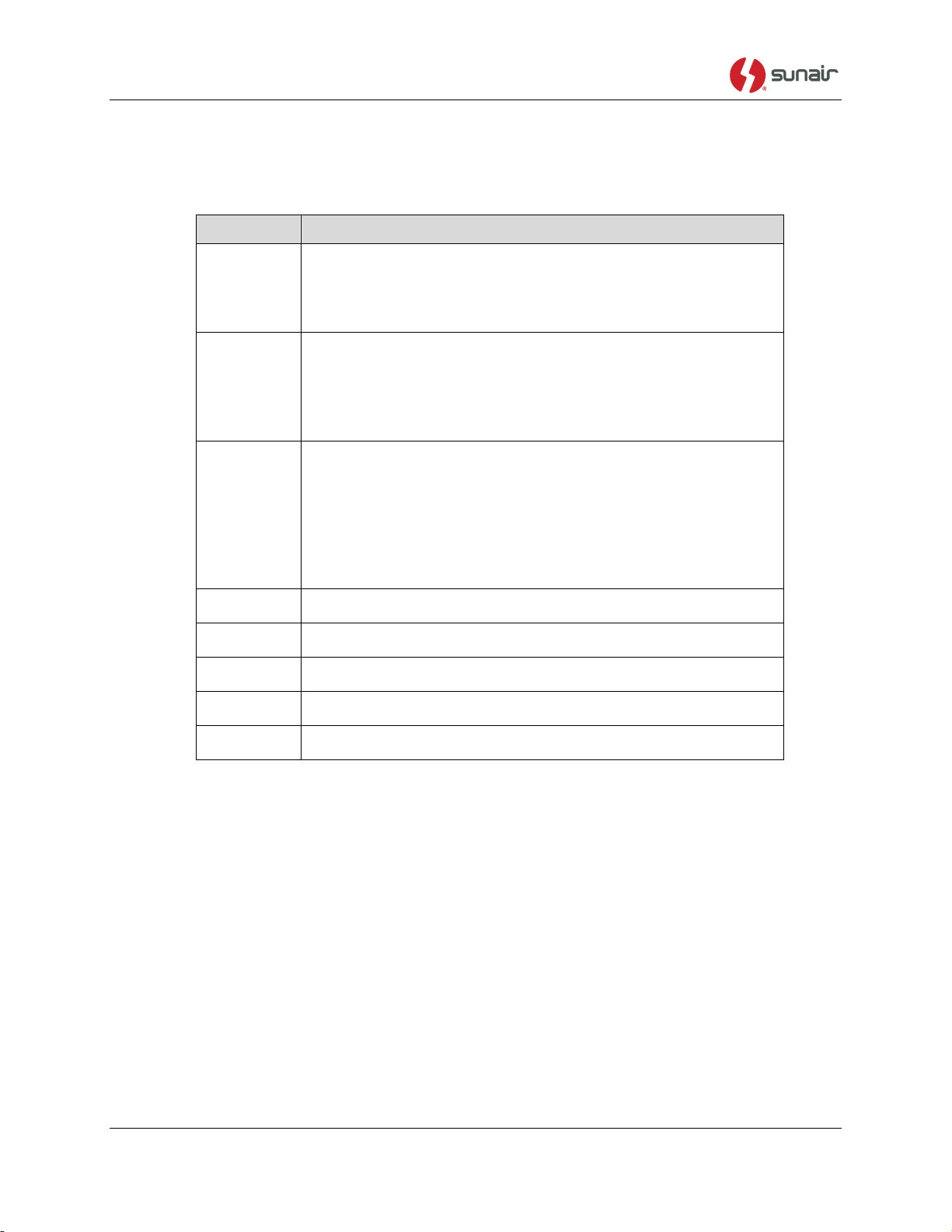
CU-9150
Switch
Function
8
Setting this switch to the UP position enables the keyline
detector circuitry. This function is currently unsupported by
the CPU software, so this switch should always be set to the
DOWN position.
7
Setting this switch to the UP position stops the CPU from
going into powerdown mode after tuning or changing
channels. This switch should be in the up position when
using the Display Board in the TS-9150 Diagnostic Test Set,
but should be set to the DOWN position for normal operation.
6
Setting this switch to the UP position causes the coupler to
allow more time for the relays to change state. As the relays
age, they take longer to change state. Try setting this switch
to the UP position on couplers which start to indicate tune
failures intermittently and which have been in service for
several years. The tune timeout changes from 10 seconds to
17 seconds when this switch is set.
5
Not used.
4
Not used.
3
Not used.
2
Not used.
1
Not used.
After making a change to the DIP switch settings, a CPU reset is required to make the change
effective. This can be done by pressing S101 on the CPU board or by powering the system down
and then up again.
Table 5.7-1 S201 DIP Switch Settings
5-10 Use or disclosure of information from this document is subject to the restrictions
indicated on the proprietary/confidentiality page of this document.
Page 59
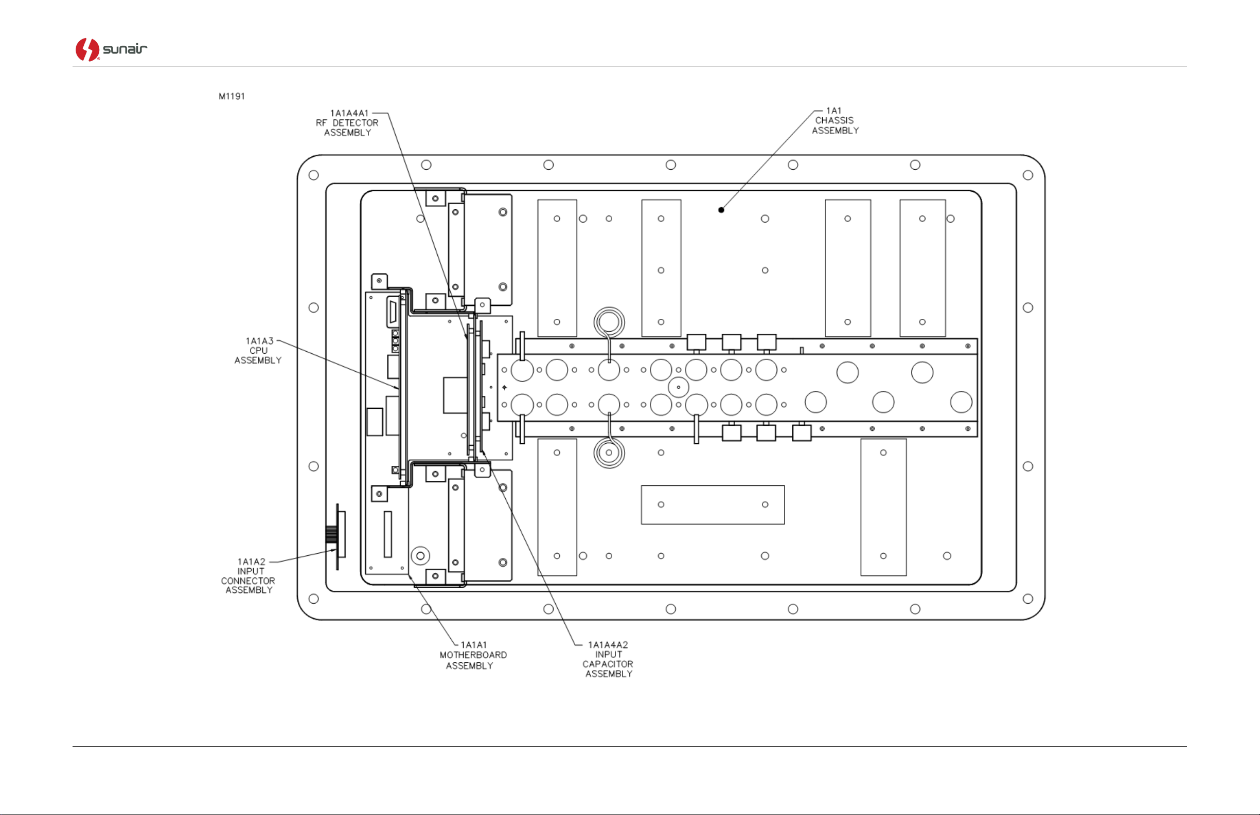
CU-9150
Figure 5.7-1 CU-9150 Assembly Locations
Use or disclosure of information from this document is subject to the restrictions 5-11
indicated on the proprietary/confidentiality page of this document.
Page 60
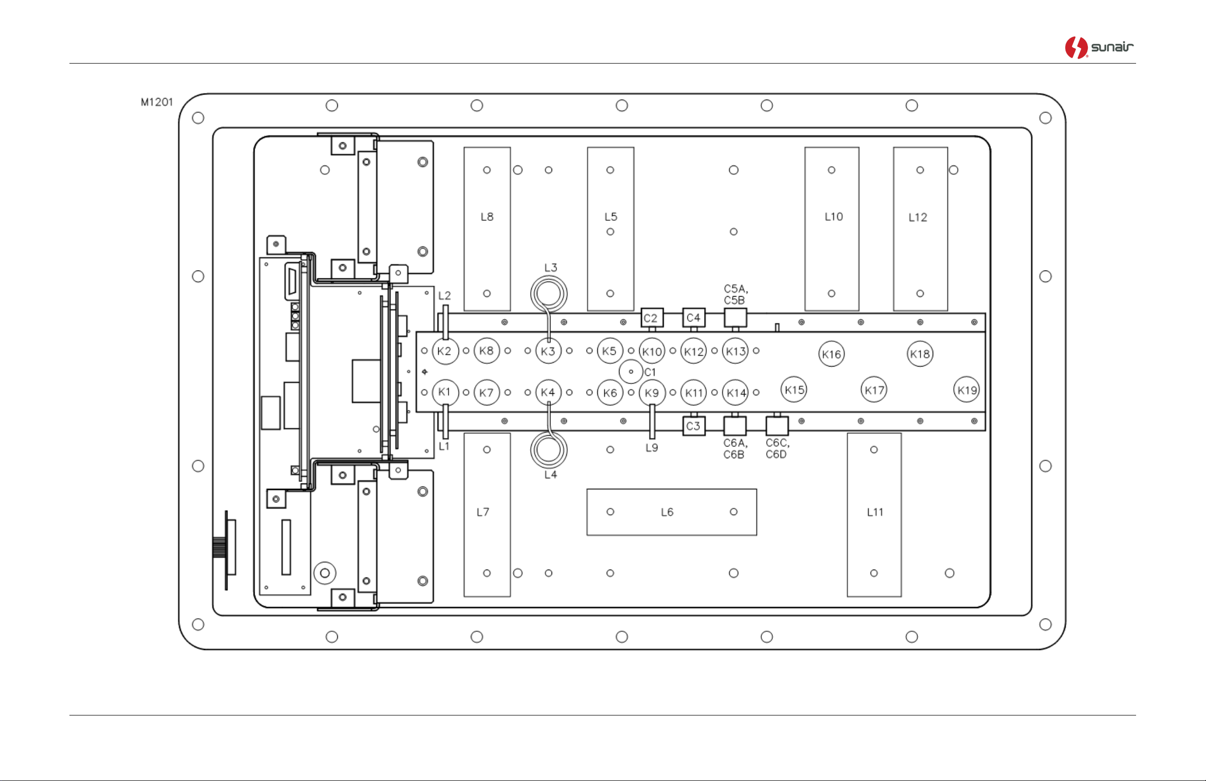
CU-9150
Figure 5.7-2 1A1 Chassis Component Locations
5-12 Use or disclosure of information from this document is subject to the restrictions
indicated on the proprietary/confidentiality page of this document.
Page 61
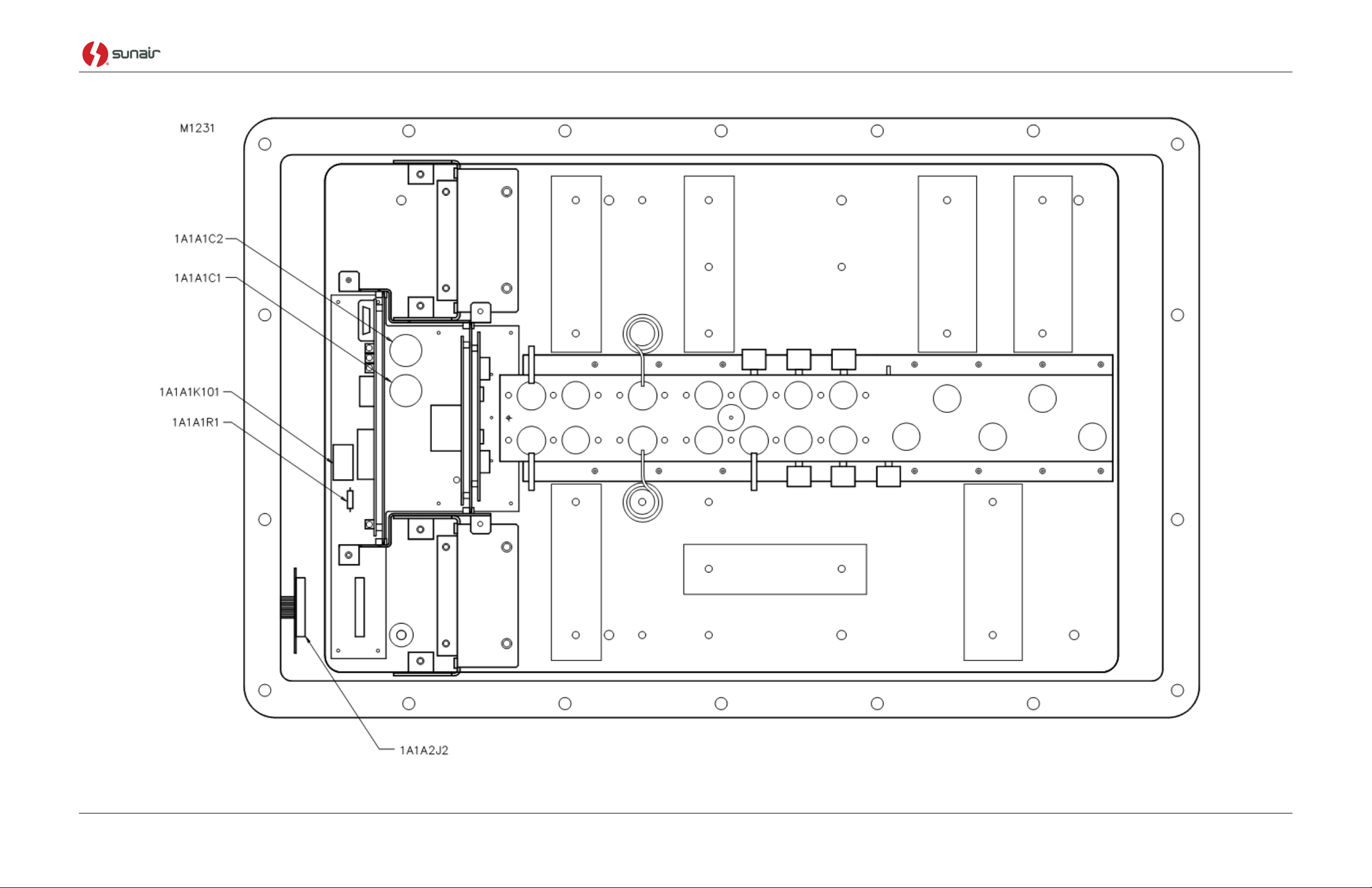
CU-9150
Figure 5.7-3. Non-Chassis Component Locations
Use or disclosure of information from this document is subject to the restrictions 5-13
indicated on the proprietary/confidentiality page of this document.
Page 62
CU-9150
FINAL ASSEMBLY TESTED CU-9150
FINAL ASSY,TESTED,GRAY CU-9150
8120001257
WASHER, SPLIT #6
0500040001
WASHER, SPLIT #10
0500070008
WASHER, FLAT #10 .500 OD
0500220000
WASHER, FLAT .250 ID .500 OD
0500330000
SCREW, PH 6-32 X 5/16 LG.
0500890056
SCREW, PH 10-32 X 1 LG.
0500940169
CAPLUG NO. EC-10
0508270006
CAPLUG NO. EC-28
0508740002
WASHER, SPLIT 1/4
0538370009
LABEL, WARNING, HI-VOLTAGE
1003030009
CORD, O-RING, .210 DIA NEOPR
1006990038
SCREW, 1/4-20 X 5/8, PHIL
1013400020
COVER, ANTENNA COUPLER, GRY
8104010514
GASKET, FLAT, WELDMENT, CASE
8120001265
FINAL ASSY, GRAY, CU-9150
8120001354
PROTECTIVE COVER, CLEAR
8120018109
INNER COVER
8120018206
1A1
CHASSIS ASSY, KW CPLR
8120010094
FINAL ASSEMBLY CU-9150
FINAL ASSY, GRAY, CU-9150
8120001354
LUG, SOLDER, PLAIN .625 ID
0501830006
VALVE, BREATHER
1000090035
SIGN, WARNING, RF RADIATION
1006240004
COAX, SHIELDED, RG-142 B/U
1008460010
CONNECTOR, RF, BNC, UG-913
1008460036
CLIP, 34 PIN SOCKET RETAINER
1013430026
INSULATOR, SLEEVE, RF
6029102303
RING, RETAINER
6029102401
WELDMENT, CASE, GRY
8092010412
NAMEPLATE, CU-9150
8120003004
1A1
CHASSIS ASSY, KW CPLR
8120010094
1A1A2
PC ASSY, INPUT CONNECTOR
8120019091
1A1A4A1
PC ASSY. RF DETECTOR
8120020090
1A1A3
PC ASSY, CPU
8120030095
1A1A3U
301
EPROM W/CU-9150 SOFTWARE U301
8120033299
1A1A4A2
PC ASSY, INPUT CAPACITOR
8120042093
CHASSIS ASSEMBLY 1A1
CHASSIS ASSY
8120010094
C1
CAPACITOR,15 PF
1013220021
C2
CAP. 25PF, 7.5KV, NPO
0290320003
C3
CAP. 50PF, 7.5KV, NPO
0290200008
C4
CAPACITOR,100 PF,7.5 KV NPO
1012740030
C5A
CAPACITOR,100 PF,7.5 KV NPO
1012740030
C5B
CAPACITOR,100 PF,7.5 KV NPO
1012740030
C6A
CAPACITOR,100 PF,7.5 KV NPO
1012740030
C6B
CAPACITOR,100 PF,7.5 KV NPO
1012740030
C6C
CAPACITOR,100 PF,7.5 KV NPO
1012740030
C6D
CAPACITOR,100 PF,7.5 KV NPO
1012740030
C7
CAP. 0.1 UF, 50V, X7R
1011180014
C8
CAP. 0.1 UF, 50V, X7R
1011180014
FAN1
FAN, 24VDC, MUFFIN XL-DC
1009130005
FAN2
FAN, 24VDC, MUFFIN XL-DC
1009130005
K1
RELAY, VACUUM, K44P334
1013210026
K2
RELAY, VACUUM, K44P334
1013210026
K3
RELAY, VACUUM, K44P334
1013210026
K4
RELAY, VACUUM, K44P334
1013210026
K5
RELAY, VACUUM, K44P334
1013210026
K6
RELAY, VACUUM, K44P334
1013210026
K7
RELAY, VACUUM, K44P334
1013210026
K8
RELAY, VACUUM, K44P334
1013210026
K9
RELAY, VACUUM, K44P334
1013210026
K10
RELAY, VACUUM, K44P334
1013210026
K11
RELAY, VACUUM, K44P334
1013210026
K12
RELAY, VACUUM, K44P334
1013210026
K13
RELAY, VACUUM, K44P334
1013210026
K14
RELAY, VACUUM, K44P334
1013210026
K15
RELAY, VACUUM, KC-12
1013200021
K16
RELAY, VACUUM, KC-12
1013200021
K17
RELAY, VACUUM, KC-12
1013200021
K18
RELAY, VACUUM, KC-12
1013200021
K19
RELAY, VACUUM, KC-12
1013200021
L1
INDUCTOR, 0.05 UHY
8120013204
L2
INDUCTOR, 0.1 UHY
8120013701
L3
INDUCTOR, 0.2 UHY
8120018095
L4
INDUCTOR, 0.4 UHY
8120017099
L5
INDUCTOR ASSY, 0.8 UHY
8120016092
L6
INDUCTOR ASSY, 1.6 UHY
8120015096
L7
INDUCTOR ASSY, 3.2 UHY
8120014090
CHASSIS ASSEMBLY 1A1 (Continued)
CHASSIS ASSY (Continued)
8120010094
L8
INDUCTOR ASSY, 6.4 UHY
8120013093
L9
INDUCTOR, 0.025 UHY
8120012704
L10
INDUCTOR ASSY, 12.6 UHY
8120012097
L11
INDUCTOR ASSY, 25.2 UHY
8120011091
L12
INDUCTOR ASSY, 25.2 UHY
8120011091
ROD, THD. 1/4-20,.875LG
1009280007
STRAP, COPPER, 1/2W, .030 THK
1012730034
TERMINAL, RING, FOR 1/4 STUD
1012790037
STANDOFF, F-F, 6-32 .690 L
6035142109
STANDOFF, F-F, 1/4-20, 3.19 L
8092016500
BRACKET FAN
8120012577
BRACKET, PC ASSY, LEFT
8120013506
BRACKET,PC ASSY, RIGHT
8120013603
PLATE, CHASSIS
8120015207
GROUND BAR, CHASSIS
8120015304
BRACKET, RELAY MOUNTING
8120015401
STANDOFF,COIL MOUNT
8120016505
RF DETECTOR/INPUT CAPACITOR ASSEMBLY 1A1A4
RF DETECTOR/ INPUT CAPACITOR
ASSY
8120920091
WASHER, SPLIT #4 SS DNP
0500020001
WASHER, FLAT #4 .81 OD DNP
0500180008
SCREW, PH 4-40 X 5/16 LG. DNP
0500850054
1A1A4A1
PC ASSY, RF DETECTOR.
8120020090
1A1A4A2
PC ASSY , INPUT CAPACITOR
8120042093
LONG WIRE ADAPTER KIT 1A1A5
ADAPTER KIT, LONG-WIRE
ANTENNA
8120909003
C1
CAP. 100PF, 15KV, N750
0275470008
C2
CAP. 100PF, 15KV, N750
0275470008
WASHER, SPLIT #10
0500070008
WASHER, FLAT #10 .500 OD
0500220000
SCREW, HEX HD 10-32 X 7/16 LG.
0526570075
BAG, PLASTIC 3 X 5 X 4MZ DNP
0841251011
PLATE, CAPACITOR MTG., ANT.
8092012806
PLATE, CAPACITOR MTG., NTWK.
8092012903
WHIP/LONG-WIRE ID PLATE
8120909011
Table 5.7-2 CU-9150 Detailed Assemblies List
5-14 Use or disclosure of information from this document is subject to the restrictions
indicated on the proprietary/confidentiality page of this document.
Page 63
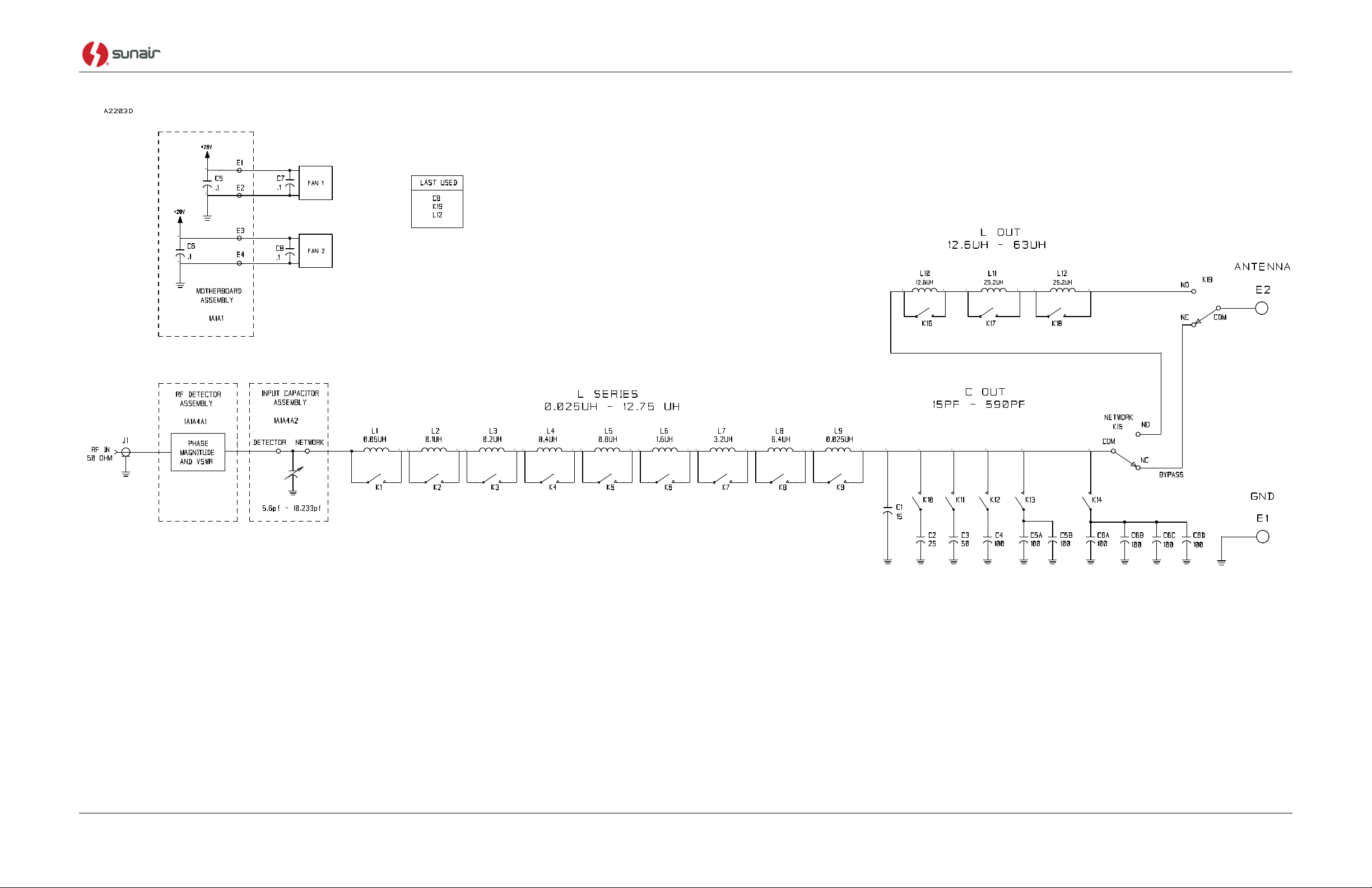
CU-9150
Figure 5.7-4. Final Assembly Tested CU-9150, Chassis Assembly 1A1 and Long Wire Adapter Kit 1A1A5
(Page 1 of 2)
Use or disclosure of information from this document is subject to the restrictions 5-15
indicated on the proprietary/confidentiality page of this document.
Page 64
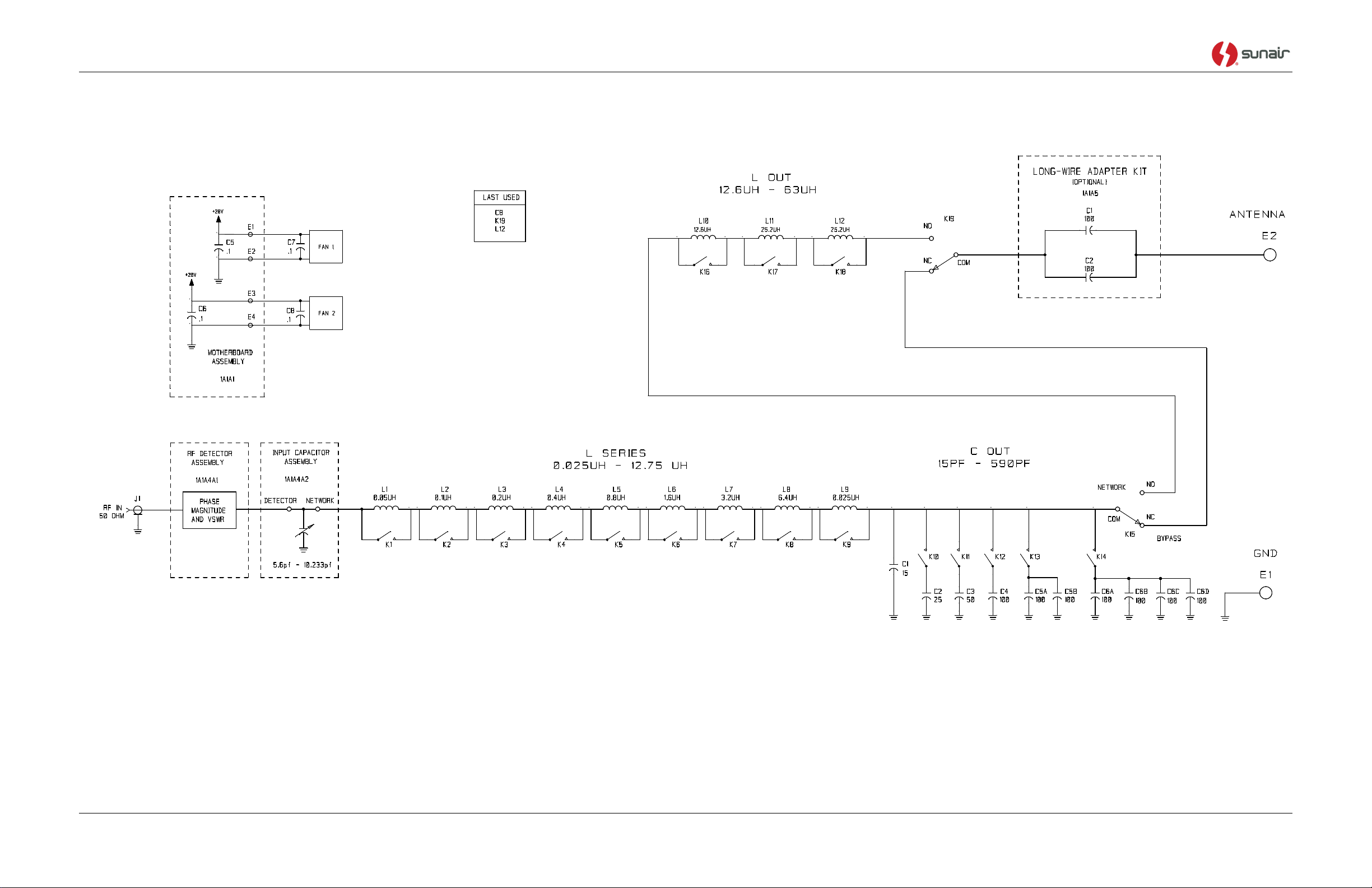
CU-9150
Figure 5.7-4. Final Assembly Tested CU-9150, Chassis Assembly 1A1 and Long Wire Adapter Kit 1A1A5
(Page 2 of 2)
5-16 Use or disclosure of information from this document is subject to the restrictions
indicated on the proprietary/confidentiality page of this document.
Page 65
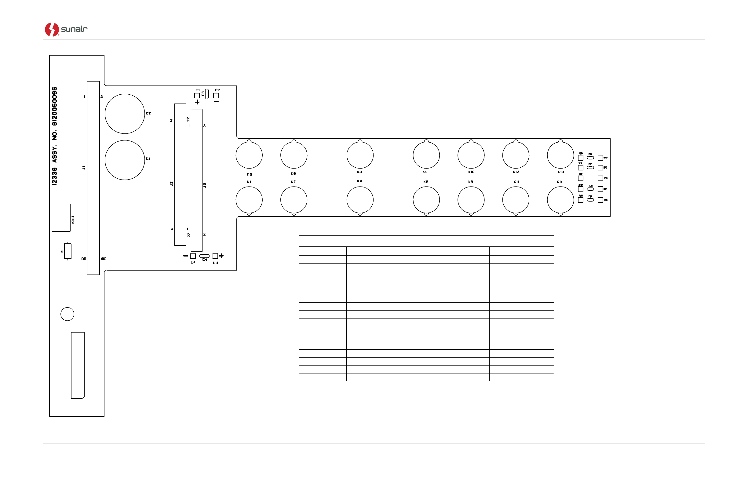
CU-9150
PC ASSEMBLY, CU-9150 MOTHERBOARD, 1A1A1
PC ASSY, MOTHER BOARD
8120050096
C1
CAP. 6800UF, 63V, 105C
1010800019
C2
CAP. 6800UF, 63V, 105C
1010800019
C3
CAP. 0.1UF, 50V, X7R
1011180014
C4
CAP. 0.1UF, 50V, X7R
1011180014
C5
CAP. 0.01UF, 50V, X7R, 20%
0281730008
C6
CAP. 0.01UF, 50V, X7R, 20%
0281730008
C7
CAP. 0.01UF, 50V, X7R, 20%
0281730008
C8
CAP. 0.01UF, 50V, X7R, 20%
0281730008
J1
CONNECTOR, PCB, 100 PIN
1013190025
J2
CONNECTOR, PC, 22PIN DUAL,FEM
1008830003
J3
CONNECTOR, PC, 22PIN DUAL,FEM
1008830003
K101
RELAY, SPST, 24VDC, PC MOUNT
1010310038
P1
CONNECTOR, RIBBON, 34 PIN, FEM
1012090035
R1
RESISTOR 3, 5%, 3W
1004600003
XP1
CONNECTOR, TRANSITION, 34PIN
1012040038
CABLE, RIBBON, 34 COND. 28AWG
1011900025
Use or disclosure of information from this document is subject to the restrictions 5-17
indicated on the proprietary/confidentiality page of this document.
Figure 5.7-5. PC Assembly, CU-9150 Motherboard, 1A1A1
(Page 1 of 3)
Page 66
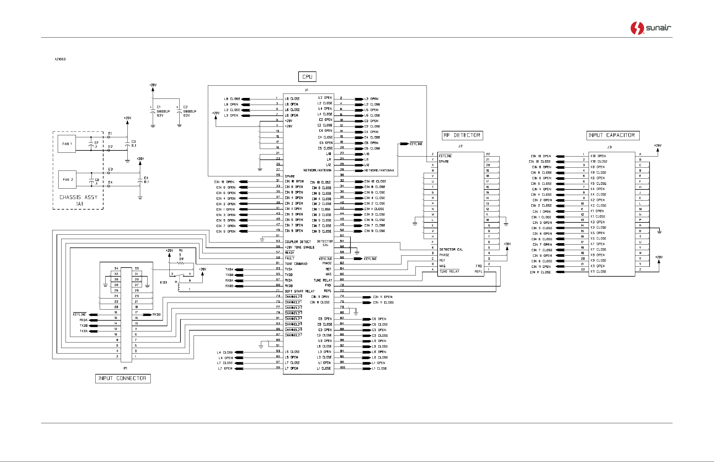
CU-9150
Figure 5.7-5. PC Assembly, CU-9150 Motherboard, 1A1A1
(Page 2 of 3)
5-18 Use or disclosure of information from this document is subject to the restrictions
indicated on the proprietary/confidentiality page of this document.
Page 67
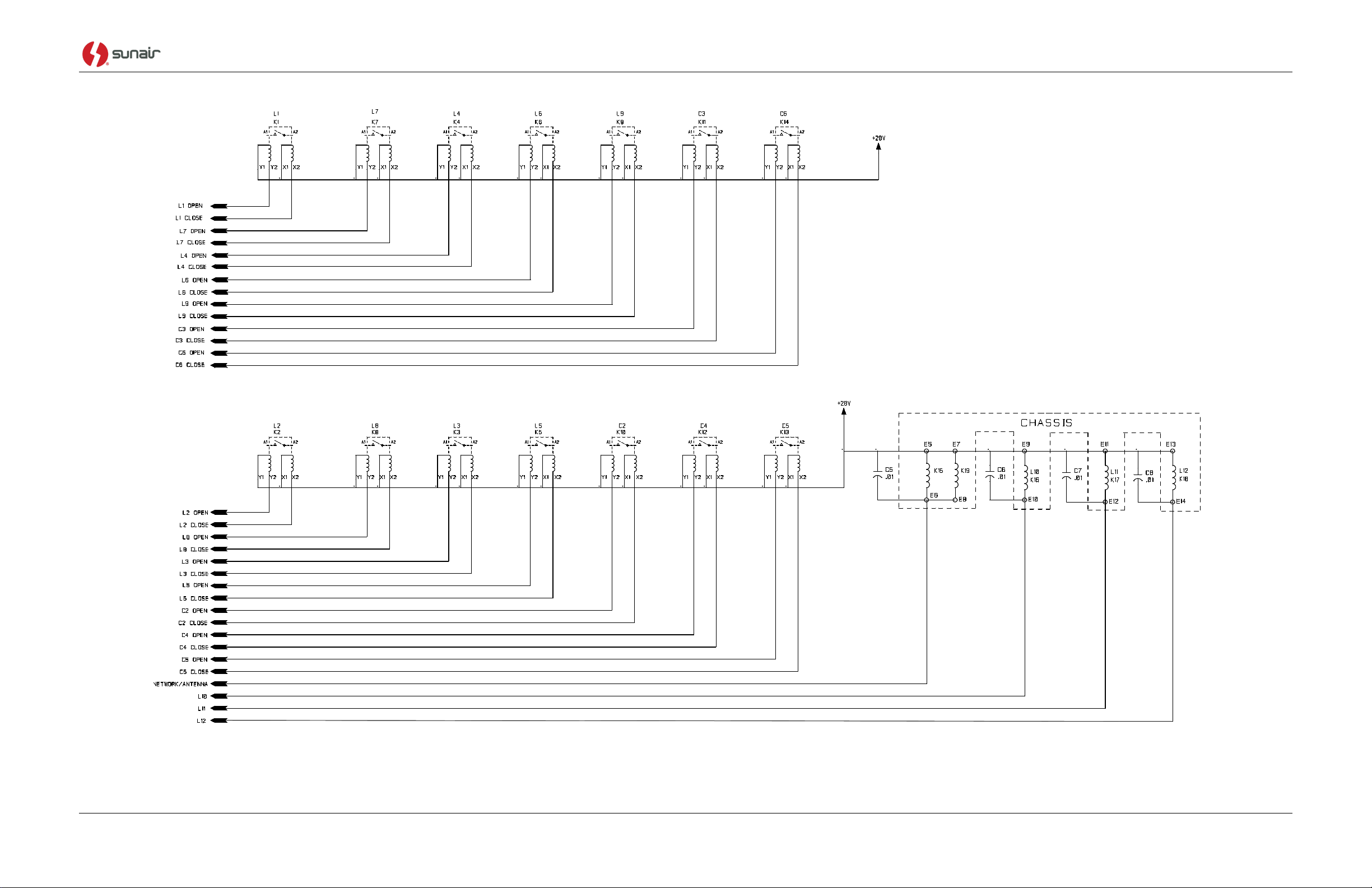
CU-9150
Figure 5.7-5. PC Assembly, CU-9150 Motherboard, 1A1A1
(Page 3 of 3)
Use or disclosure of information from this document is subject to the restrictions 5-19
indicated on the proprietary/confidentiality page of this document.
Page 68

CU-9150
THIS PAGE INTENTIONALLY LEFT BLANK
5-20 Use or disclosure of information from this document is subject to the restrictions
indicated on the proprietary/confidentiality page of this document.
Page 69
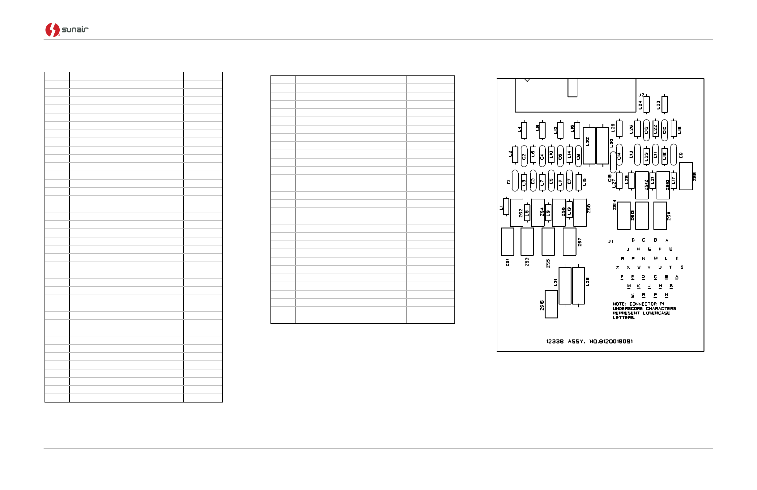
CU-9150
PC ASSEMBLY, INPUT CONNECTOR, 1A1A2
PC ASSY, INPUT CONNECTOR
8120019091
C1
CAP 0.1UF, 50V, X7R, 20%
0281610002
C2
CAP 0.1UF, 50V, X7R, 20%
0281610002
C3
CAP 0.1UF, 50V, X7R, 20%
0281610002
C4
CAP 0.1UF, 50V, X7R, 20%
0281610002
C5
CAP 0.1UF, 50V, X7R, 20%
0281610002
C6
CAP 0.1UF, 50V, X7R, 20%
0281610002
C7
CAP 0.1UF, 50V, X7R, 20%
0281610002
C8
CAP 0.1UF, 50V, X7R, 20%
0281610002
C9
CAP 0.1UF, 50V, X7R, 20%
0281610002
C10
CAP 0.1UF, 50V, X7R, 20%
0281610002
C11
CAP 0.1UF, 50V, X7R, 20%
0281610002
C12
CAP 0.1UF, 50V, X7R, 20%
0281610002
C13
CAP 0.1UF, 50V, X7R, 20%
0281610002
C14
CAP 0.1UF, 50V, X7R, 20%
0281610002
C15
CAP 0.1UF, 50V, X7R, 20%
0281610002
J1
CONNECTOR, POWER, 37 PIN ROUND
1009330004
J2
CONNECTOR, HEADER, 34 PIN MALE
1011880024
L1
INDUCTOR, MOLDED, 22UH, 10%
0664060005
L2
INDUCTOR, MOLDED, 22UH, 10%
0664060005
L3
INDUCTOR, MOLDED, 22UH, 10%
0664060005
L4
INDUCTOR, MOLDED, 22UH, 10%
0664060005
L5
INDUCTOR, MOLDED, 22UH, 10%
0664060005
L6
INDUCTOR, MOLDED, 22UH, 10%
0664060005
L7
INDUCTOR, MOLDED, 22UH, 10%
0664060005
L8
INDUCTOR, MOLDED, 22UH, 10%
0664060005
L9
INDUCTOR, MOLDED, 22UH, 10%
0664060005
L10
INDUCTOR, MOLDED, 22UH, 10%
0664060005
L11
INDUCTOR, MOLDED, 22UH, 10%
0664060005
L12
INDUCTOR, MOLDED, 22UH, 10%
0664060005
L13
INDUCTOR, MOLDED, 22UH, 10%
0664060005
L14
INDUCTOR, MOLDED, 22UH, 10%
0664060005
L15
INDUCTOR, MOLDED, 22UH, 10%
0664060005
L16
INDUCTOR, MOLDED, 22UH, 10%
0664060005
L17
INDUCTOR, MOLDED, 22UH, 10%
0664060005
L18
INDUCTOR, MOLDED, 22UH, 10%
0664060005
L19
INDUCTOR, MOLDED, 22UH, 10%
0664060005
L20
INDUCTOR, MOLDED, 22UH, 10%
0664060005
L21
INDUCTOR, MOLDED, 22UH, 10%
0664060005
L22
INDUCTOR, MOLDED, 22UH, 10%
0664060005
L23
INDUCTOR, MOLDED, 22UH, 10%
0664060005
L24
INDUCTOR, MOLDED, 22UH, 10%
0664060005
L25
INDUCTOR, MOLDED, 22UH, 10%
0664060005
L26
INDUCTOR, MOLDED, 22UH, 10%
0664060005
L27
INDUCTOR, MOLDED, 22UH, 10%
0664060005
L28
INDUCTOR, MOLDED, 22UH, 10%
0664060005
L29
INDUCTOR, MOLDED, 6.8UH, 10%
0652200001
L30
INDUCTOR, MOLDED, 6.8UH, 10%
0652200001
L31
INDUCTOR, MOLDED, 6.8UH, 10%
0652200001
L32
INDUCTOR, MOLDED, 6.8UH, 10%
0652200001
ZS1
VARISTOR, V56RA8
1013360028
ZS2
VARISTOR, V56RA8
1013360028
ZS3
VARISTOR, V56RA8
1013360028
ZS4
VARISTOR, V56RA8
1013360028
ZS5
VARISTOR, V56RA8
1013360028
ZS6
VARISTOR, V56RA8
1013360028
ZS7
VARISTOR, V56RA8
1013360028
ZS8
VARISTOR, V56RA8
1013360028
ZS9
VARISTOR, V56RA8
1013360028
ZS10
VARISTOR, V56RA8
1013360028
ZS11
VARISTOR, V56RA8
1013360028
ZS12
VARISTOR, V56RA8
1013360028
ZS13
VARISTOR, V56RA8
1013360028
ZS14
VARISTOR, V56RA8
1013360028
ZS15
VARISTOR, V56RA8
1013360028
WASHER, SPLIT #6
0500040001
WASHER, FLAT #6 .312 OD
0500200009
SCREW, PH 6-32 X 1/4 LG.
0500890048
SCREW, PH 6-32 X 3/8 LG.
0500890064
STANDOFF, M-F, 6-32 .375 L
0542930005
Use or disclosure of information from this document is subject to the restrictions 5-21
indicated on the proprietary/confidentiality page of this document.
Figure 5.7-6. PC Assembly, Input Connector, 1A1A2
(Page 1 of 2)
Page 70
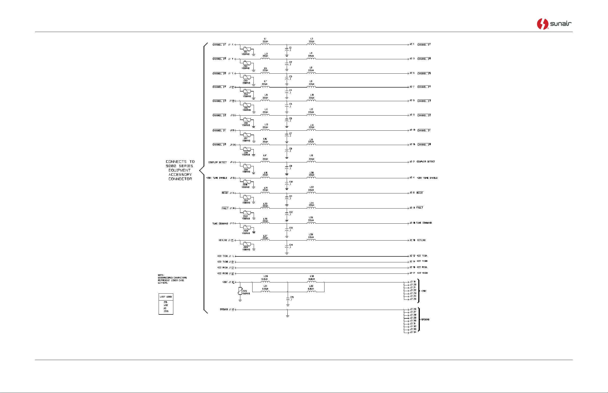
CU-9150
Figure 5.7-6. PC Assembly, Input Connector, 1A1A2
(Page 2 of 2)
5-22 Use or disclosure of information from this document is subject to the restrictions
indicated on the proprietary/confidentiality page of this document.
Page 71
CU-9150
PC ASSEMBLY, INPUT CONNECTOR, 1A1A2
PC ASSEMBLY, CPU
8120030095
C101
CAP. 10UF, 20V
1007290005
C102
CAP. 0.1UF, 50V, X7R
1011180014
C103
CAP. 1UF, 35V
0281660000
C104
CAP. 0.01UF, 50V, X7R, 20%
0281730008
C105
CAP. 0.01UF, 50V, X7R, 20%
0281730008
C106
CAP. 0.01UF, 50V, X7R, 20%
0281730008
C107
CAP. 0.01UF, 50V, X7R, 20%
0281730008
C108
CAP. 0.01UF, 50V, X7R, 20%
0281730008
C109
CAP. 0.01UF, 50V, X7R, 20%
0281730008
C110
CAP. 0.01UF, 50V, X7R, 20%
0281730008
C111
CAP. 0.01UF, 50V, X7R, 20%
0281730008
C112
CAP. 0.01UF, 50V, X7R, 20%
0281730008
C113
CAP. 0.01UF, 50V, X7R, 20%
0281730008
C114
CAP. 0.01UF, 50V, X7R, 20%
0281730008
C115
CAP. 0.01UF, 50V, X7R, 20%
0281730008
C116
CAP. 22PF, 200V, NPO, 5%
1012902200
C117
CAP. 22PF, 200V, NPO, 5%
1012902200
C118
CAP. 0.01UF, 50V, X7R, 20%
0281730008
C119
CAP. 0.01UF, 50V, X7R, 20%
0281730008
C120
CAP. 0.01UF, 50V, X7R, 20%
0281730008
C121
CAP. 0.01UF, 50V, X7R, 20%
0281730008
C122
CAP. 0.01UF, 50V, X7R, 20%
0281730008
C123
CAP. 1UF, 35V
0281660000
C124
CAP. 0.01UF, 50V, X7R, 20%
0281730008
C201
CAP. 0.1UF, 50V, X7R
1011180014
C205
CAP. 0.01UF, 50V, X7R, 20%
0281730008
C206
CAP. 0.01UF, 50V, X7R, 20%
0281730008
C207
CAP. 0.01UF, 50V, X7R, 20%
0281730008
C208
CAP. 0.01UF, 50V, X7R, 20%
0281730008
C209
CAP. 0.01UF, 50V, X7R, 20%
0281730008
C210
CAP. 0.01UF, 50V, X7R, 20%
0281730008
C211
CAP. 0.01UF, 50V, X7R, 20%
0281730008
C212
CAP. 0.01UF, 50V, X7R, 20%
0281730008
C213
CAP. 0.01UF, 50V, X7R, 20%
0281730008
C214
CAP. 6.8UF, 20V
0296780006
C215
CAP. 0.01UF, 50V, X7R, 20%
0281730008
C217
CAP. 0.1UF, 50V, X7R
1011180014
C218
CAP. 0.01UF, 50V, X7R, 20%
0281730008
C219
CAP. 22UF, 15V
0281690006
C220
CAP. 0.01UF, 50V, X7R, 20%
0281730008
C301
CAP. 0.01UF, 50V, X7R, 20%
0281730008
C302
CAP. 10UF, 20V
1007290005
C303
CAP. 0.01UF, 50V, X7R, 20%
0281730008
C304
CAP. 0.01UF, 50V, X7R, 20%
0281730008
C305
CAP. 0.01UF, 50V, X7R, 20%
0281730008
C306
CAP. 0.01UF, 50V, X7R, 20%
0281730008
C307
CAP. 0.01UF, 50V, X7R, 20%
0281730008
C308
CAP. 0.01UF, 50V, X7R, 20%
0281730008
C309
CAP. 0.01UF, 50V, X7R, 20%
0281730008
C310
CAP. 0.01UF, 50V, X7R, 20%
0281730008
C311
CAP. 0.01UF, 50V, X7R, 20%
0281730008
C312
CAP. 0.01UF, 50V, X7R, 20%
0281730008
C313
CAP. 0.1UF, 50V, X7R
1011180014
C401
CAP. 0.01UF, 50V, X7R, 20%
0281730008
C402
CAP. 0.01UF, 50V, X7R, 20%
0281730008
C403
CAP. 0.01UF, 50V, X7R, 20%
0281730008
C404
CAP. 0.01UF, 50V, X7R, 20%
0281730008
C405
CAP. 0.01UF, 50V, X7R, 20%
0281730008
C406
CAP. 0.01UF, 50V, X7R, 20%
0281730008
C407
CAP. 0.01UF, 50V, X7R, 20%
0281730008
C408
CAP. 0.01UF, 50V, X7R, 20%
0281730008
C409
CAP. 0.01UF, 50V, X7R, 20%
0281730008
C410
CAP. 0.01UF, 50V, X7R, 20%
0281730008
C411
CAP. 0.01UF, 50V, X7R, 20%
0281730008
C412
CAP. 0.01UF, 50V, X7R, 20%
0281730008
C413
CAP. 0.01UF, 50V, X7R, 20%
0281730008
C414
CAP. 0.01UF, 50V, X7R, 20%
0281730008
C415
CAP. 0.01UF, 50V, X7R, 20%
0281730008
C416
CAP. 0.01UF, 50V, X7R, 20%
0281730008
C417
CAP. 0.01UF, 50V, X7R, 20%
0281730008
C418
CAP. 0.01UF, 50V, X7R, 20%
0281730008
C419
CAP. 0.01UF, 50V, X7R, 20%
0281730008
C420
CAP. 0.01UF, 50V, X7R, 20%
0281730008
C421
CAP. 0.01UF, 50V, X7R, 20%
0281730008
C422
CAP. 0.01UF, 50V, X7R, 20%
0281730008
C423
CAP. 0.01UF, 50V, X7R, 20%
0281730008
C424
CAP. 0.01UF, 50V, X7R, 20%
0281730008
C425
CAP. 0.01UF, 50V, X7R, 20%
0281730008
C426
CAP. 0.01UF, 50V, X7R, 20%
0281730008
C427
CAP. 0.01UF, 50V, X7R, 20%
0281730008
C428
CAP. 0.01UF, 50V, X7R, 20%
0281730008
C429
CAP. 0.01UF, 50V, X7R, 20%
0281730008
C430
CAP. 0.01UF, 50V, X7R, 20%
0281730008
C431
CAP. 0.01UF, 50V, X7R, 20%
0281730008
C432
CAP. 0.01UF, 50V, X7R, 20%
0281730008
C433
CAP. 0.01UF, 50V, X7R, 20%
0281730008
C434
CAP. 0.01UF, 50V, X7R, 20%
0281730008
C435
CAP. 0.01UF, 50V, X7R, 20%
0281730008
C436
CAP. 0.01UF, 50V, X7R, 20%
0281730008
C437
CAP. 0.01UF, 50V, X7R, 20%
0281730008
C438
CAP. 0.01UF, 50V, X7R, 20%
0281730008
C439
CAP. 0.01UF, 50V, X7R, 20%
0281730008
C440
CAP. 0.01UF, 50V, X7R, 20%
0281730008
C441
CAP. 0.01UF, 50V, X7R, 20%
0281730008
C442
CAP. 0.01UF, 50V, X7R, 20%
0281730008
C443
CAP. 0.01UF, 50V, X7R, 20%
0281730008
C444
CAP. 0.01UF, 50V, X7R, 20%
0281730008
C445
CAP. 0.01UF, 50V, X7R, 20%
0281730008
C446
CAP. 0.01UF, 50V, X7R, 20%
0281730008
C447
CAP. 0.01UF, 50V, X7R, 20%
0281730008
C448
CAP. 0.01UF, 50V, X7R, 20%
0281730008
C449
CAP. 0.01UF, 50V, X7R, 20%
0281730008
C450
CAP. 0.01UF, 50V, X7R, 20%
0281730008
C451
CAP. 0.01UF, 50V, X7R, 20%
0281730008
C452
CAP. 0.01UF, 50V, X7R, 20%
0281730008
C453
CAP. 0.01UF, 50V, X7R, 20%
0281730008
C454
CAP. 0.01UF, 50V, X7R, 20%
0281730008
C455
CAP. 0.01UF, 50V, X7R, 20%
0281730008
C456
CAP. 0.01UF, 50V, X7R, 20%
0281730008
C457
CAP. 0.01UF, 50V, X7R, 20%
0281730008
C458
CAP. 0.01UF, 50V, X7R, 20%
0281730008
C459
CAP. 0.01UF, 50V, X7R, 20%
0281730008
C501
CAP. 0.01UF, 50V, X7R, 20%
0281730008
C502
CAP. 0.01UF, 50V, X7R, 20%
0281730008
C503
CAP. 0.01UF, 50V, X7R, 20%
0281730008
C504
CAP. 0.01UF, 50V, X7R, 20%
0281730008
C505
CAP. 0.01UF, 50V, X7R, 20%
0281730008
C506
CAP. 0.01UF, 50V, X7R, 20%
0281730008
C507
CAP. 0.01UF, 50V, X7R, 20%
0281730008
C508
CAP. 0.01UF, 50V, X7R, 20%
0281730008
C509
CAP. 0.01UF, 50V, X7R, 20%
0281730008
C510
CAP. 0.01UF, 50V, X7R, 20%
0281730008
C511
CAP. 0.01UF, 50V, X7R, 20%
0281730008
C512
CAP. 0.01UF, 50V, X7R, 20%
0281730008
C513
CAP. 0.01UF, 50V, X7R, 20%
0281730008
C514
CAP. 0.01UF, 50V, X7R, 20%
0281730008
C515
CAP. 0.01UF, 50V, X7R, 20%
0281730008
C516
CAP. 0.01UF, 50V, X7R, 20%
0281730008
C517
CAP. 0.01UF, 50V, X7R, 20%
0281730008
C518
CAP. 0.01UF, 50V, X7R, 20%
0281730008
C519
CAP. 0.01UF, 50V, X7R, 20%
0281730008
C520
CAP. 0.01UF, 50V, X7R, 20%
0281730008
C521
CAP. 0.01UF, 50V, X7R, 20%
0281730008
Use or disclosure of information from this document is subject to the restrictions 5-23
indicated on the proprietary/confidentiality page of this document.
Figure 5.7-7. PC Assembly, CPU, 1A1A3
(Page 1 of 10)
Page 72
CU-9150
PC ASSEMBLY, INPUT CONNECTOR, 1A1A2 (Continued)
C522
CAP. 0.01UF, 50V, X7R, 20%
0281730008
C523
CAP. 0.01UF, 50V, X7R, 20%
0281730008
C524
CAP. 0.01UF, 50V, X7R, 20%
0281730008
C525
CAP. 0.01UF, 50V, X7R, 20%
0281730008
C526
CAP. 0.01UF, 50V, X7R, 20%
0281730008
C527
CAP. 0.01UF, 50V, X7R, 20%
0281730008
C528
CAP. 0.01UF, 50V, X7R, 20%
0281730008
C529
CAP. 0.01UF, 50V, X7R, 20%
0281730008
C530
CAP. 0.01UF, 50V, X7R, 20%
0281730008
C531
CAP. 0.01UF, 50V, X7R, 20%
0281730008
C532
CAP. 0.01UF, 50V, X7R, 20%
0281730008
C533
CAP. 0.01UF, 50V, X7R, 20%
0281730008
C534
CAP. 0.01UF, 50V, X7R, 20%
0281730008
C535
CAP. 0.01UF, 50V, X7R, 20%
0281730008
C536
CAP. 0.01UF, 50V, X7R, 20%
0281730008
C537
CAP. 0.01UF, 50V, X7R, 20%
0281730008
C538
CAP. 0.01UF, 50V, X7R, 20%
0281730008
C539
CAP. 0.01UF, 50V, X7R, 20%
0281730008
C540
CAP. 0.01UF, 50V, X7R, 20%
0281730008
C541
CAP. 0.1UF, 50V, X7R
1011180014
C542
CAP. 0.1UF, 50V, X7R
1011180014
C543
CAP. 0.1UF, 50V, X7R
1011180014
C544
CAP. 0.1UF, 50V, X7R
1011180014
C545
CAP. 0.01UF, 50V, X7R, 20%
0281730008
C546
CAP. 0.01UF, 50V, X7R, 20%
0281730008
C547
CAP. 0.01UF, 50V, X7R, 20%
0281730008
C548
CAP. 0.01UF, 50V, X7R, 20%
0281730008
C549
CAP. 0.01UF, 50V, X7R, 20%
0281730008
C550
CAP. 0.01UF, 50V, X7R, 20%
0281730008
C551
CAP. 0.01UF, 50V, X7R, 20%
0281730008
C552
CAP. 0.01UF, 50V, X7R, 20%
0281730008
C553
CAP. 0.01UF, 50V, X7R, 20%
0281730008
C554
CAP. 0.01UF, 50V, X7R, 20%
0281730008
C557
CAP. 0.01UF, 50V, X7R, 20%
0281730008
C558
CAP. 0.01UF, 50V, X7R, 20%
0281730008
C559
CAP. 0.01UF, 50V, X7R, 20%
0281730008
C560
CAP. 0.01UF, 50V, X7R, 20%
0281730008
C561
CAP. 0.01UF, 50V, X7R, 20%
0281730008
C562
CAP. 0.01UF, 50V, X7R, 20%
0281730008
C563
CAP. 0.01UF, 50V, X7R, 20%
0281730008
C564
CAP. 0.01UF, 50V, X7R, 20%
0281730008
C565
CAP. 0.01UF, 50V, X7R, 20%
0281730008
C566
CAP. 0.01UF, 50V, X7R, 20%
0281730008
C601
CAP. 1UF, 35V
0281660000
C602
CAP. 0.1UF, 50V, X7R
1011180014
C603
CAP. 0.01UF, 50V, X7R, 20%
0281730008
C604
CAP. 0.1UF, 50V, X7R
1011180014
C605
CAP. 6.8UF, 20V
0296780006
C606
CAP. 0.1UF, 50V, X7R
1011180014
C607
CAP. 0.01UF, 50V, X7R, 20%
0281730008
C608
CAP. 0.1UF, 50V, X7R
1011180014
C609
CAP. 0.01UF, 50V, X7R, 20%
0281730008
C610
CAP. 68UF, 15V
0296540005
C611
CAP. 0.01UF, 50V, X7R, 20%
0281730008
C612
CAP. 1000UF, 35V, 105C
1011420031
C613
CAP. 0.01UF, 50V, X7R, 20%
0281730008
C614
CAP. 0.01UF, 50V, X7R, 20%
0281730008
C616
CAP. 0.01UF, 50V, X7R, 20%
0281730008
C617
CAP. 0.01UF, 50V, X7R, 20%
0281730008
C618
CAP. 0.01UF, 50V, X7R, 20%
0281730008
C619
CAP. 0.01UF, 50V, X7R, 20%
0281730008
C620
CAP. 0.01UF, 50V, X7R, 20%
0281730008
C621
CAP. 0.01UF, 50V, X7R, 20%
0281730008
C622
CAP. 0.01UF, 50V, X7R, 20%
0281730008
C623
CAP. 0.01UF, 50V, X7R, 20%
0281730008
C624
CAP. 0.01UF, 50V, X7R, 20%
0281730008
C625
CAP. 0.01UF, 50V, X7R, 20%
0281730008
C626
CAP. 0.01UF, 50V, X7R, 20%
0281730008
C628
CAP. 0.01UF, 50V, X7R, 20%
0281730008
C629
CAP. 0.01UF, 50V, X7R, 20%
0281730008
C630
CAP. 0.01UF, 50V, X7R, 20%
0281730008
C631
CAP. 0.01UF, 50V, X7R, 20%
0281730008
C632
CAP. 0.01UF, 50V, X7R, 20%
0281730008
CP601
CAP. NTWK. 0.1UF, 10 PIN
1006580018
CP602
CAP. NTWK. 0.1UF, 10 PIN
1006580018
CR101
DIODE, SIGNAL, SIL. 1N4454
0405270003
CR201
DIODE, SIGNAL, SIL. 1N4454
0405270003
CR301
DIODE, LED, AMBER 550-2305
1011480000
CR302
DIODE, LED, GREEN 550-2205
1011030012
CR303
DIODE, LED, RED 550-2405
1008480029
CR304
DIODE, LED, RED 550-2405
1008480029
CR305
DIODE, SIGNAL, SIL. 1N4454
0405270003
CR401
DIODE, RECTIFIER 1N4004
0405180004
CR402
DIODE, RECTIFIER 1N4004
0405180004
CR403
DIODE, RECTIFIER 1N4004
0405180004
CR404
DIODE, RECTIFIER 1N4004
0405180004
CR501
DIODE, TRANSIENT SUP. 1.5KA18A
1010960032
CR502
DIODE, TRANSIENT SUP. 1.5KA18A
1010960032
CR503
DIODE, TRANSIENT SUP. 1.5KA18A
1010960032
CR504
DIODE, TRANSIENT SUP. 1.5KA18A
1010960032
CR601
DIODE, ZENER 1N5245B
0405210001
CR602
DIODE, ZENER 1N5343B
1003060005
J1
CONNECTOR, DB-9, FEMALE RT ANG
1012550028
L103
INDUCTOR, MOLDED, 8.2UH, 5%
0652060005
L104
INDUCTOR, MOLDED, 8.2UH, 5%
0652060005
L106
INDUCTOR, MOLDED, 47UH, 5%
0652680003
L201
INDUCTOR, MOLDED, 47UH, 5%
0652680003
L202
INDUCTOR, MOLDED, 47UH, 5%
0652680003
L203
INDUCTOR, MOLDED, 47UH, 5%
0652680003
L204
INDUCTOR, MOLDED, 47UH, 5%
0652680003
L301
INDUCTOR, MOLDED, 47UH, 5%
0652680003
L302
INDUCTOR, MOLDED, 47UH, 5%
0652680003
L303
INDUCTOR, MOLDED, 47UH, 5%
0652680003
L304
INDUCTOR, MOLDED, 47UH, 5%
0652680003
L305
INDUCTOR, MOLDED, 47UH, 5%
0652680003
L401
INDUCTOR, MOLDED, 2.7UH, 5%
0652180001
L402
INDUCTOR, MOLDED, 2.7UH, 5%
0652180001
L403
INDUCTOR, MOLDED, 2.7UH, 5%
0652180001
L404
INDUCTOR, MOLDED, 2.7UH, 5%
0652180001
L405
INDUCTOR, MOLDED, 2.7UH, 5%
0652180001
L406
INDUCTOR, MOLDED, 2.7UH, 5%
0652180001
L407
INDUCTOR, MOLDED, 2.7UH, 5%
0652180001
L408
INDUCTOR, MOLDED, 2.7UH, 5%
0652180001
L409
INDUCTOR, MOLDED, 2.7UH, 5%
0652180001
L410
INDUCTOR, MOLDED, 2.7UH, 5%
0652180001
L411
INDUCTOR, MOLDED, 2.7UH, 5%
0652180001
L412
INDUCTOR, MOLDED, 2.7UH, 5%
0652180001
L413
INDUCTOR, MOLDED, 2.7UH, 5%
0652180001
L414
INDUCTOR, MOLDED, 2.7UH, 5%
0652180001
L415
INDUCTOR, MOLDED, 2.7UH, 5%
0652180001
L416
INDUCTOR, MOLDED, 2.7UH, 5%
0652180001
L417
INDUCTOR, MOLDED, 2.7UH, 5%
0652180001
L418
INDUCTOR, MOLDED, 2.7UH, 5%
0652180001
L419
INDUCTOR, MOLDED, 2.7UH, 5%
0652180001
L420
INDUCTOR, MOLDED, 2.7UH, 5%
0652180001
L421
INDUCTOR, MOLDED, 2.7UH, 5%
0652180001
L422
INDUCTOR, MOLDED, 2.7UH, 5%
0652180001
L423
INDUCTOR, MOLDED, 10UH, 5%
0650240006
L424
INDUCTOR, MOLDED, 10UH, 5%
0650240006
L425
INDUCTOR, MOLDED, 10UH, 5%
0650240006
L426
INDUCTOR, MOLDED, 10UH, 5%
0650240006
L601
INDUCTOR, MOLDED, 47UH, 5%
0652680003
L602
INDUCTOR, MOLDED, 47UH, 5%
0652680003
L603
INDUCTOR, MOLDED, 47UH, 5%
0652680003
Figure 5.7-7. PC Assembly, CPU, 1A1A3
(Page 2 of 10)
5-24 Use or disclosure of information from this document is subject to the restrictions
indicated on the proprietary/confidentiality page of this document.
Page 73
CU-9150
PC ASSEMBLY, INPUT CONNECTOR, 1A1A2 (Continued)
L604
INDUCTOR, MOLDED, 47UH, 5%
0652680003
L605
INDUCTOR, MOLDED, 47UH, 5%
0652680003
L606
INDUCTOR, MOLDED, 47UH, 5%
0652680003
L607
INDUCTOR, MOLDED, 47UH, 5%
0652680003
L608
INDUCTOR, MOLDED, 47UH, 5%
0652680003
L609
INDUCTOR, MOLDED, 10UH, 5%
0650240006
Q101
TRANSISTOR, N-CH, FET 2N7000
1011050013
Q201
TRANSISTOR, N-CH, FET 2N7000
1011050013
Q301
TRANSISTOR, PNP, SI. 2N2907A
0448390001
Q302
TRANSISTOR, N-CH, FET 2N7000
1011050013
Q401
TRANSISTOR, N-CH, FET MTP3055E
1010750011
Q402
TRANSISTOR, N-CH, FET MTP3055E
1010750011
Q403
TRANSISTOR, N-CH, FET MTP3055E
1010750011
Q404
TRANSISTOR, N-CH, FET MTP3055E
1010750011
R101
RESISTOR 2.7K, 5%, 1/8W
1010802721
R102
RESISTOR 10K, 5%, 1/8W
1010801031
R103
RESISTOR 470, 5%, 1/8W
1010804715
R104
RESISTOR 47K, 5%, 1/8W
1010804731
R105
RESISTOR 4.7K, 5%, 1/8W
1010804723
R106
RESISTOR 0.0, 0%, 1/4W
1011600021
R107
RESISTOR 10K, 5%, 1/8W
1010801031
R108
RESISTOR 10K, 5%, 1/8W
1010801031
R109
RESISTOR 47K, 5%, 1/8W
1010804731
R110
RESISTOR 10K, 5%, 1/8W
1010801031
R112
RESISTOR 0.0, 0%, 1/4W
1011600021
R202
RESISTOR 10K, 5%, 1/8W
1010801031
R203
RESISTOR 10K, 5%, 1/8W
1010801031
R204
RESISTOR 47K, 5%, 1/8W
1010804731
R205
RESISTOR 4.7K, 5%, 1/8W
1010804723
R206
RESISTOR 47K, 5%, 1/8W
1010804731
R207
RESISTOR 10K, 5%, 1/8W
1010801031
R208
RESISTOR 47K, 5%, 1/8W
1010804731
R209
RESISTOR 10K, 5%, 1/8W
1010801031
R210
RESISTOR 10, 5%, 1/8W
1010801007
R211
RESISTOR 0.0, 0%, 1/4W
1011600021
R213
RESISTOR 22, 5%, 1/8W
1010802208
R214
RESISTOR 10, 5%, 1/8W
1010801007
R302
RESISTOR 0.0, 0%, 1/4W
1011600021
R304
RESISTOR 2.7K, 10%, 1/2W
0165780002
R305
RESISTOR PTC
1012680011
R306
RESISTOR 47K, 5%, 1/8W
1010804731
R307
RESISTOR PTC
1012680011
R308
RESISTOR 10K, 5%, 1/8W
1010801031
R309
RESISTOR 47K, 5%, 1/8W
1010804731
R401
RESISTOR 47K, 5%, 1/8W
1010804731
R402
RESISTOR 47K, 5%, 1/8W
1010804731
R403
RESISTOR 47K, 5%, 1/8W
1010804731
R404
RESISTOR 47K, 5%, 1/8W
1010804731
R501
RESISTOR 4.7, 5%, 1/4W
1001060024
R502
RESISTOR 4.7, 5%, 1/4W
1001060024
R503
RESISTOR 4.7, 5%, 1/4W
1001060024
R504
RESISTOR 4.7, 5%, 1/4W
1001060024
R505
RESISTOR 4.7, 5%, 1/4W
1001060024
R506
RESISTOR 4.7, 5%, 1/4W
1001060024
R507
RESISTOR 4.7, 5%, 1/4W
1001060024
R508
RESISTOR 4.7, 5%, 1/4W
1001060024
R509
RESISTOR 4.7, 5%, 1/4W
1001060024
R510
RESISTOR 4.7, 5%, 1/4W
1001060024
R511
RESISTOR 4.7, 5%, 1/4W
1001060024
R512
RESISTOR 4.7, 5%, 1/4W
1001060024
R513
RESISTOR 4.7, 5%, 1/4W
1001060024
R514
RESISTOR 4.7, 5%, 1/4W
1001060024
R515
RESISTOR 4.7, 5%, 1/4W
1001060024
R516
RESISTOR 4.7, 5%, 1/4W
1001060024
R517
RESISTOR 4.7, 5%, 1/4W
1001060024
R518
RESISTOR 4.7, 5%, 1/4W
1001060024
R519
RESISTOR 4.7, 5%, 1/4W
1001060024
R520
RESISTOR 4.7, 5%, 1/4W
1001060024
R521
RESISTOR 4.7, 5%, 1/4W
1001060024
R522
RESISTOR 4.7, 5%, 1/4W
1001060024
R523
RESISTOR 4.7, 5%, 1/4W
1001060024
R524
RESISTOR 4.7, 5%, 1/4W
1001060024
R525
RESISTOR 4.7, 5%, 1/4W
1001060024
R526
RESISTOR 4.7, 5%, 1/4W
1001060024
R527
RESISTOR 4.7, 5%, 1/4W
1001060024
R528
RESISTOR 4.7, 5%, 1/4W
1001060024
R601
RESISTOR 0.0, 0%, 1/4W
1011600021
RP101
RES NTWK 10 PIN SIP 10K COM
1006130021
RP201
RES NTWK 10 PIN SIP 10K COM
1006130021
RP601
RES NTWK 10 PIN SIP 10K COM
1006130021
S101
SWITCH, PUSHBUTTON,SPST
1010710001
S201
SWITCH, SPST, DIP, 8 POSITION
1012930033
U101
IC DIGITAL, MAX 490
1013240022
U102
IC. DIGITAL TL7705B
1012210006
U103
IC. DIGITAL, CPU 80C188EB-8
1012580008
U104
IC. LINEAR LM2903
1011410036
U105
PAL W/CU-9150 PAL SFTWRE U105
8120033698
U107
IC. DIGITAL 74HC373
1006480030
U108
IC. DIGITAL 74HC373
1006480030
U109
IC. DIGITAL 74HC245
1006470034
U202
IC. DIGITAL 74HC138
1006480013
U203
IC. DIGITAL 74HC138
1006480013
U204
IC. DIGITAL 74HC04
1010280023
U205
IC. DIGITAL 74HC74
1008000019
U206
IC. DIGITAL 74HC244
1006460039
U207
IC. LINEAR MC34072
1011440032
U208
IC. DIGITAL, 12 BIT A/D W/MUX
1013380029
U302
IC. DIGITAL, RAM 551001
1012600009
U303
IC. DIGITAL 28C64
1010660004
U304
IC,DIGITAL, UCN5842A
1012530035
U401
IC. DIGITAL UCN-5801A
1011800021
U402
IC. DIGITAL UCN-5801A
1011800021
U403
IC. DIGITAL UCN-5801A
1011800021
U404
IC. DIGITAL 74HC374
1006450033
U405
IC. DIGITAL MC14504
1006090037
U501
IC,DIGITAL, UCN5842A
1012530035
U502
IC,DIGITAL, UCN5842A
1012530035
U503
IC,DIGITAL, UCN5842A
1012530035
U504
IC,DIGITAL, UCN5842A
1012530035
U601
IC. DIGITAL 74HC688
1009050001
U602
IC. DIGITAL 74HC14
1006490027
U603
IC. DIGITAL 74HC14
1006490027
U604
IC. DIGITAL 74HC374
1006450033
U605
IC. DIGITAL 74HC244
1006460039
U606
IC. LINEAR LM340T5
0448600005
U607
IC. LINEAR LM340/7812
1003410022
XQ401
MOLDED TRANSIST0R MOUNT,TO-220
1013410025
XQ402
MOLDED TRANSIST0R MOUNT,TO-220
1013410025
XQ403
MOLDED TRANSIST0R MOUNT,TO-220
1013410025
XQ404
MOLDED TRANSIST0R MOUNT,TO-220
1013410025
XU103
SOCKET, IC, 84 PIN PLCC
1012640001
XU105
SOCKET, IC. 24 PIN SKINNY DIP
1013390024
XU301
SOCKET, IC, 32 PIN TAILLESS
1012530001
XU303
SOCKET, IC, 28 PIN TAILLESS
1006620001
Y101
CRYSTAL, 14.7456MHZ 50PPM
1013480015
WASHER, SPLIT #4
0500020001
SCREW, PH 4-40 X 1/4 LG.
0500850046
SCREW, PH 4-40 X 5/16 LG.
0500850054
WASHER, FLAT #4 .219 OD
0502560002
BACKPLANE, CPU
8120031601
Use or disclosure of information from this document is subject to the restrictions 5-25
indicated on the proprietary/confidentiality page of this document.
Figure 5.7-7. PC Assembly, CPU, 1A1A3
(Page 3 of 10)
Page 74
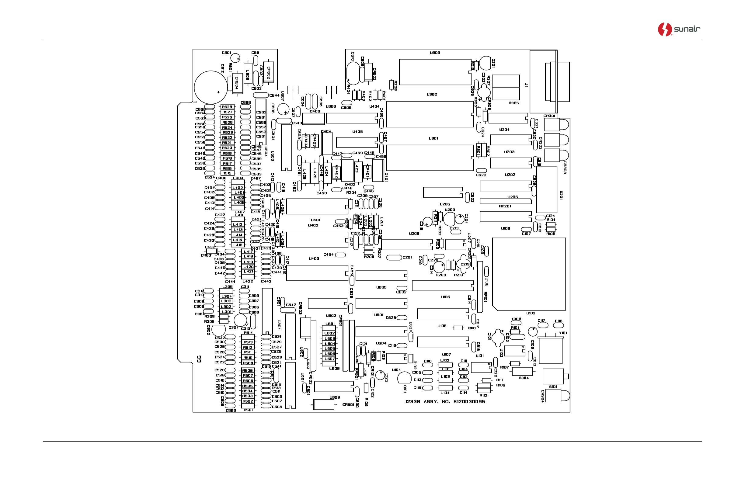
CU-9150
Figure 5.7-7. PC Assembly, CPU, 1A1A3
(Page 4 of 10)
5-26 Use or disclosure of information from this document is subject to the restrictions
indicated on the proprietary/confidentiality page of this document.
Page 75
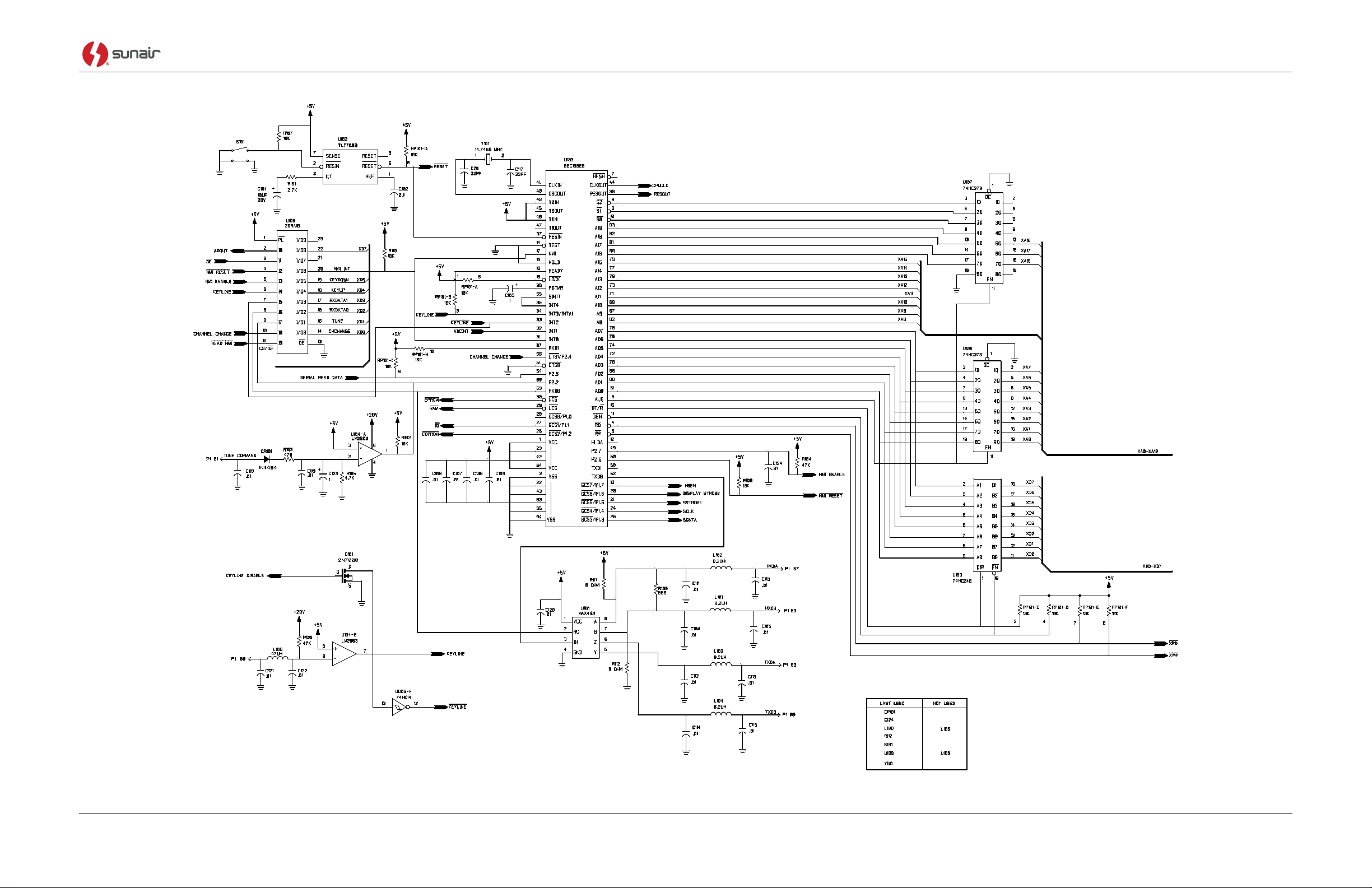
CU-9150
Figure 5.7-7. PC Assembly, CPU, 1A1A3
(Page 5 of 10)
Use or disclosure of information from this document is subject to the restrictions 5-27
indicated on the proprietary/confidentiality page of this document.
Page 76
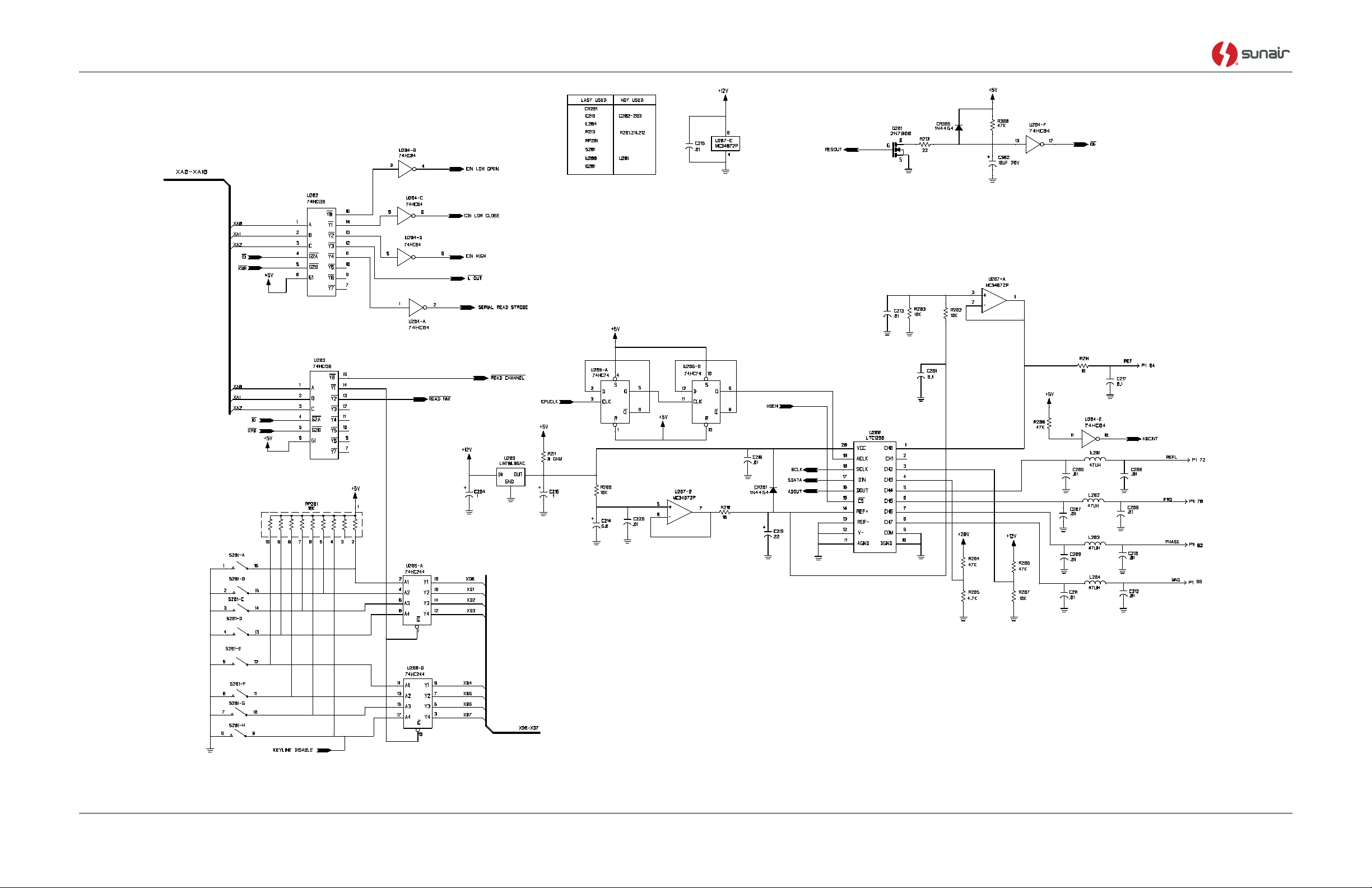
CU-9150
Figure 5.7-7. PC Assembly, CPU, 1A1A3
(Page 6 of 10)
5-28 Use or disclosure of information from this document is subject to the restrictions
indicated on the proprietary/confidentiality page of this document.
Page 77
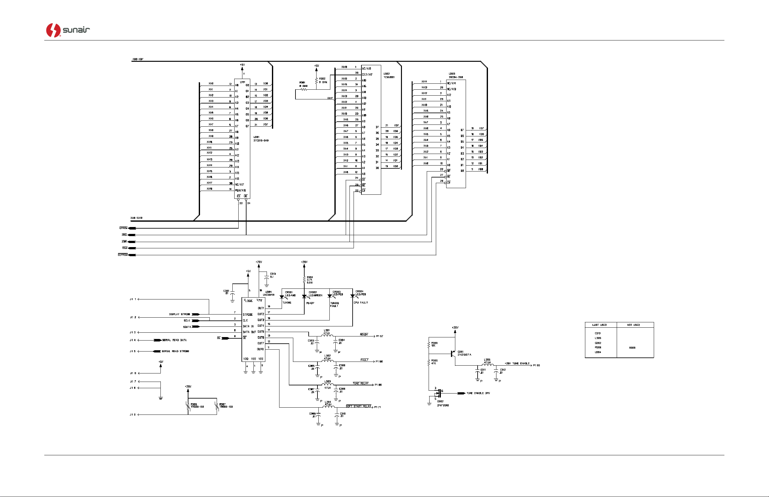
CU-9150
Figure 5.7-7. PC Assembly, CPU, 1A1A3
(Page 7 of 10)
Use or disclosure of information from this document is subject to the restrictions 5-29
indicated on the proprietary/confidentiality page of this document.
Page 78
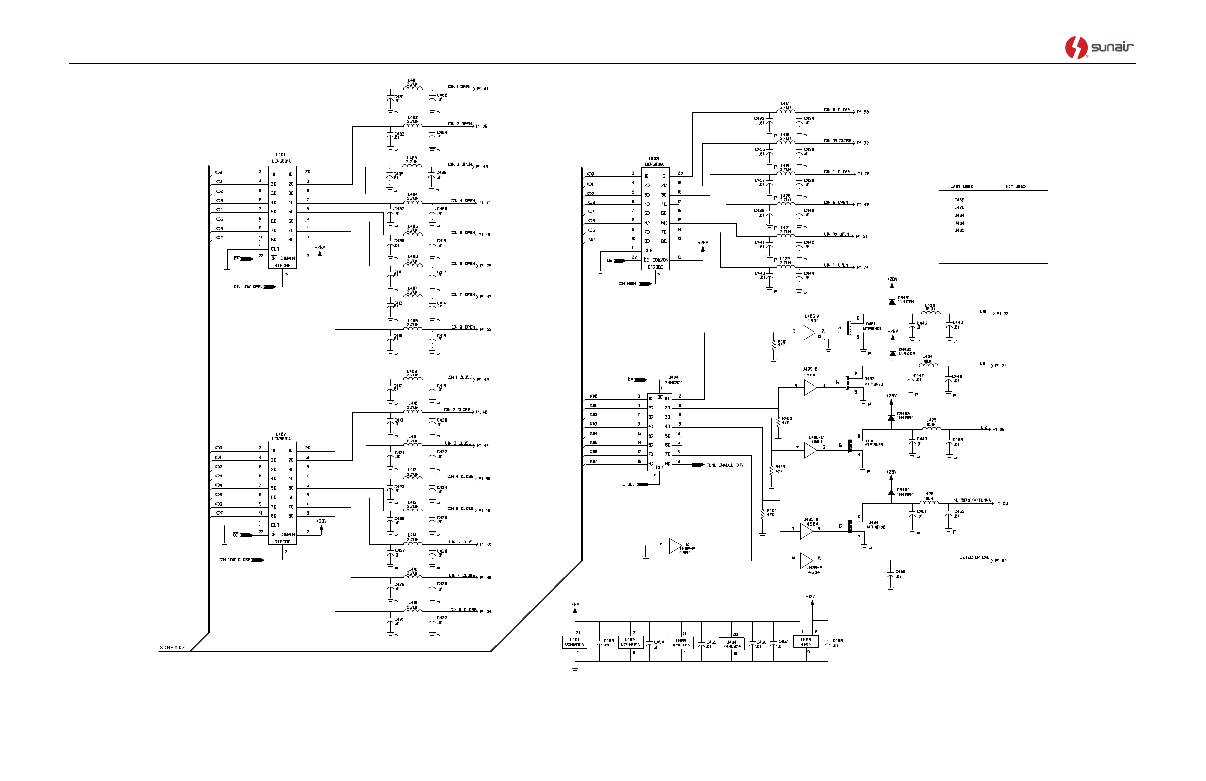
CU-9150
Figure 5.7-7. PC Assembly, CPU, 1A1A3
(Page 8 of 10)
5-30 Use or disclosure of information from this document is subject to the restrictions
indicated on the proprietary/confidentiality page of this document.
Page 79
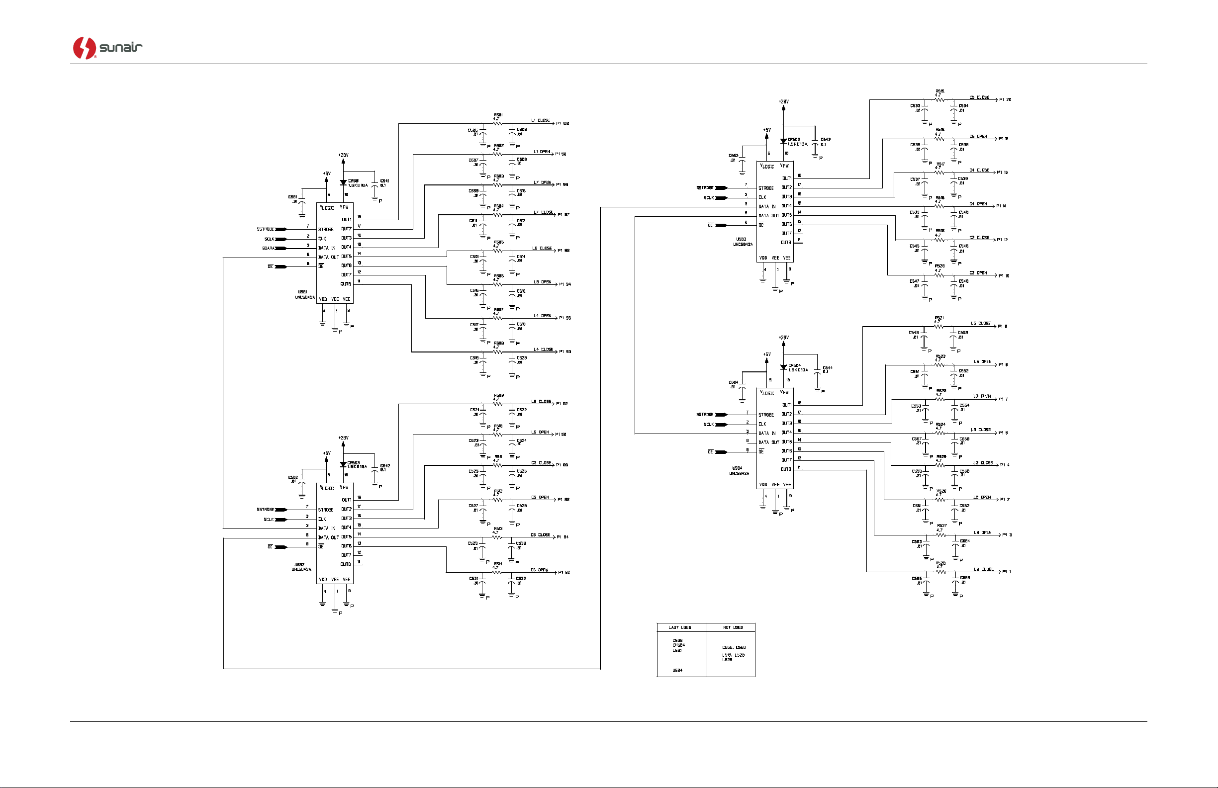
CU-9150
Figure 5.7-7. PC Assembly, CPU, 1A1A3
(Page 9 of 10)
Use or disclosure of information from this document is subject to the restrictions 5-31
indicated on the proprietary/confidentiality page of this document.
Page 80
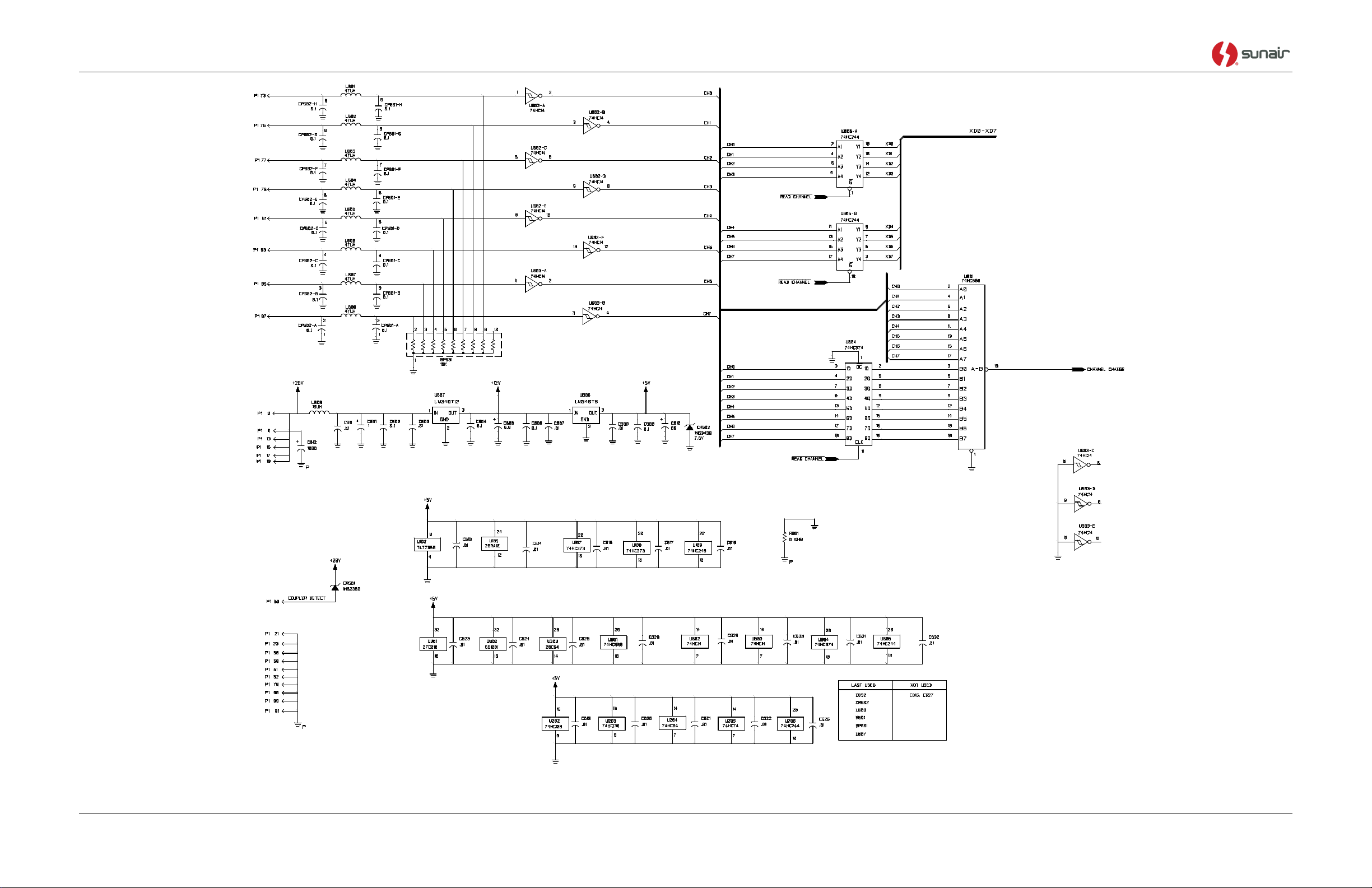
CU-9150
Figure 5.7-7. PC Assembly, CPU, 1A1A3
(Page 10 of 10)
5-32 Use or disclosure of information from this document is subject to the restrictions
indicated on the proprietary/confidentiality page of this document.
Page 81
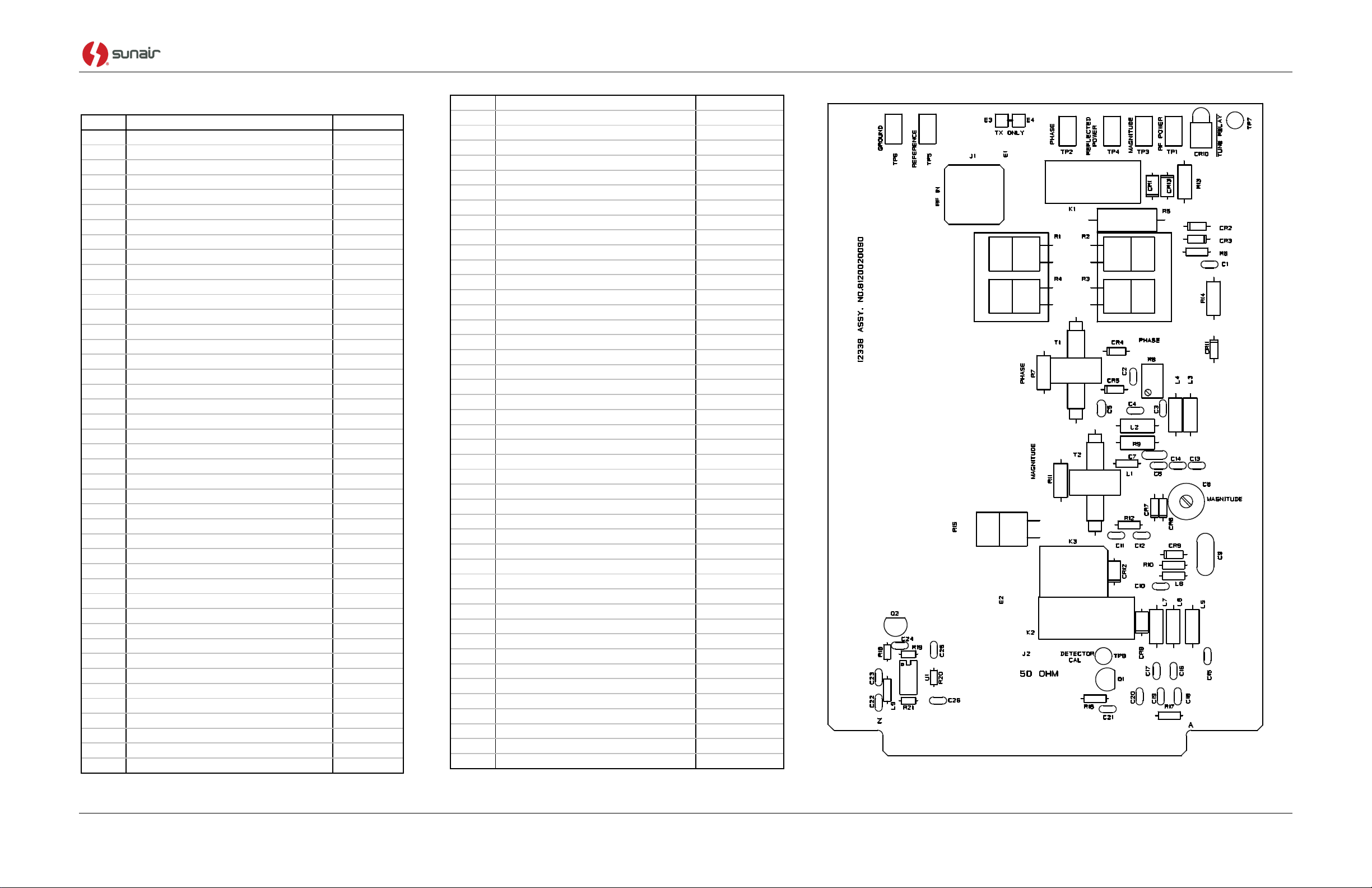
CU-9150
PC ASSEMBLY, RF DETECTOR, 1A1A4A1
PC ASSY, RF DETECTOR
8120020090
C1
CAP. 0.01UF, 50V, X7R, 20%
0281730008
C2
CAP. 0.01UF, 50V, X7R, 20%
0281730008
C3
CAP. 0.01UF, 50V, X7R, 20%
0281730008
C4
CAP. 0.01UF, 50V, X7R, 20%
0281730008
C5
CAP. 12PF, 200V NPO 5%
1012901203
C6
CAP. 0.01UF, 50V, X7R, 20%
0281730008
C7
CAP. 0.47UF, 50V, X7R, 20%
0283377771
C8
CAP. 5.5-18PF, 500V
1010020021
C9
CAP. 300PF, 500V, DM15, 2%
0282330003
C10
CAP. 0.01UF, 50V, X7R, 20%
0281730008
C11
CAP. 0.01UF, 50V, X7R, 20%
0281730008
C12
CAP. 0.01UF, 50V, X7R, 20%
0281730008
C13
CAP. 0.01UF, 50V, X7R, 20%
0281730008
C14
CAP. 0.01UF, 50V, X7R, 20%
0281730008
C15
CAP. 0.01UF, 50V, X7R, 20%
0281730008
C16
CAP. 0.01UF, 50V, X7R, 20%
0281730008
C17
CAP. 0.01UF, 50V, X7R, 20%
0281730008
C18
CAP. 0.01UF, 50V, X7R, 20%
0281730008
C19
CAP. 0.01UF, 50V, X7R, 20%
0281730008
C20
CAP. 0.01UF, 50V, X7R, 20%
0281730008
C21
CAP. 0.01UF, 50V, X7R, 20%
0281730008
C22
CAP. 0.01UF, 50V, X7R, 20%
0281730008
C23
CAP. 0.01UF, 50V, X7R, 20%
0281730008
C24
CAP. 0.001UF, 100V, X7R, 20%
0281630003
C25
CAP. 0.01UF, 50V, X7R, 20%
0281730008
C26
CAP. 0.01UF, 50V, X7R, 20%
0281730008
CR1
DIODE, RECTIFIER 1N4004
0405180004
CR2
DIODE, SIGNAL, SIL. 1N4454
0405270003
CR3
DIODE, SIGNAL, SIL. 1N4454
0405270003
CR4
DIODE, HOT CARRIER 1N6263
0405610009
CR5
DIODE, HOT CARRIER 1N6263
0405610009
CR6
DIODE, HOT CARRIER 1N6263
0405610009
CR7
DIODE, HOT CARRIER 1N6263
0405610009
CR8
DIODE, RECTIFIER 1N4004
0405180004
CR9
DIODE, HOT CARRIER 1N6263
0405610009
CR10
DIODE, LED, AMBER 550-2305
1011480000
CR11
DIODE, ZENER 1N5231B
0405390009
CR12
DIODE, RECTIFIER 1N4004
0405180004
CR13
DIODE, RECTIFIER 1N4004
0405180004
J1
CONNECTOR, RF, BNC
0753490005
K1
RELAY, SPDT, 24VDC, 10 AMP
1008290009
K2
RELAY, SPDT, 24VDC, 10 AMP
1008290009
K3
RELAY 1 FORM A 1 FORM B 24V
1012540022
L1
INDUCTOR, MOLDED, 0.47UH, 5%
0649410009
L2
INDUCTOR, MOLDED, 1000UH, 5%
0643310002
L3
INDUCTOR, MOLDED, 1000UH, 5%
0643310002
L4
INDUCTOR, MOLDED, 1000UH, 5%
0643310002
L5
INDUCTOR, MOLDED, 1000UH, 5%
0643310002
L6
INDUCTOR, MOLDED, 1000UH, 5%
0643310002
L7
INDUCTOR, MOLDED, 1000UH, 5%
0643310002
L8
INDUCTOR, MOLDED, 0.22UH, 10%
0650740009
L9
INDUCTOR, MOLDED, 47UH, 5%
0652680003
Q1
TRANSISTOR, N-CH, FET 2N7000
1011050013
Q2
TRANSISTOR, N-CH, FET 2N7000
1011050013
R1
RESISTOR, 300, 1%, 50W
1012530027
R2
RESISTOR, 9, 1%, 50W
1012520021
R3
RESISTOR, 9, 1%, 50W
1012520021
R4
RESISTOR, 300, 1%, 50W
1012530027
R5
RESISTOR 10K, 10%, 2W
0176010009
R6
RESISTOR 10K, 10%, 1/4W
0170410005
R7
RESISTOR 33, 10%, 1/2W
0171700007
R8
POT. 10K, 10%, 1/2W, 25 TURNS
1004880014
R9
RESISTOR 33, 10%, 1/2W
0171700007
R10
RESISTOR 12K, 10%, 1/4W
0183180003
R11
RESISTOR 18, 5%, 1/2W
0184730007
R12
RESISTOR 12K, 10%, 1/4W
0183180003
R13
RESISTOR 2.7K, 10%, 1/2W
0165780002
R14
RESISTOR 1K, 10%, 1/2W
0167480006
R15
RESISTOR, 50, 1%, 50W
1013420021
R16
RESISTOR 10K, 10%, 1/4W
0170410005
R17
RESISTOR 10K, 10%, 1/4W
0170410005
R18
RESISTOR 47K, 5%, 1/8W
1010804731
R19
RESISTOR 10K, 5%, 1/8W
1010801031
R20
RESISTOR 4.7K, 5%, 1/8W
1010804723
R21
RESISTOR 4.7K, 5%, 1/8W
1010804723
T1
TRANSFORMER, PHASE DETECTOR
6035040900
T2
TRANSFORMER, AMPL. DETECTOR
6035040802
TP1
TEST POINT, WHITE
0753640007
TP2
TEST POINT, WHITE
0753640007
TP3
TEST POINT, WHITE
0753640007
TP4
TEST POINT, WHITE
0753640007
TP5
TEST POINT, WHITE
0753640007
TP6
TEST POINT, WHITE
0753640007
U1
IC. LINEAR LM2903
1011410036
WASHER, SPLIT #4
0500020001
WASHER, FLAT #4 .281 OD
0500180008
SCREW, PH 4-40 X 5/16 LG.
0500850054
BACKPLANE,RF DETECTOR
8120021606
Use or disclosure of information from this document is subject to the restrictions 5-33
indicated on the proprietary/confidentiality page of this document.
Figure 5.7-8. PC Assembly, RF Detector, 1A1A4A1
(Page 1 of 2)
Page 82
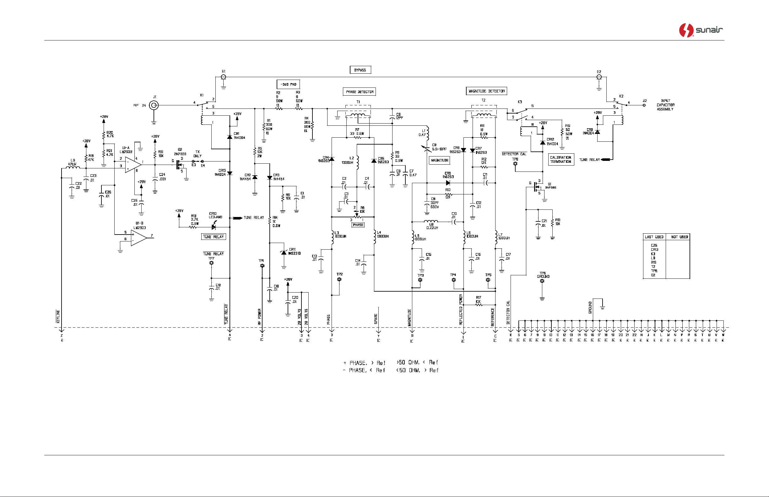
CU-9150
Figure 5.7-8. PC Assembly, RF Detector, 1A1A4A1
(Page 2 of 2)
5-34 Use or disclosure of information from this document is subject to the restrictions
indicated on the proprietary/confidentiality page of this document.
Page 83
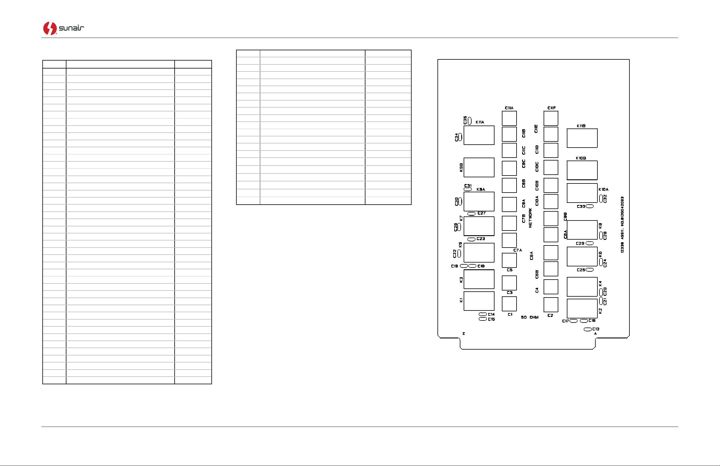
CU-9150
PC ASSEMBLY, INPUT CAPACITOR, 1A1A4A2
PC ASSY, INPUT CAPACITOR
8120042093
C1
5.6 PF 3.6 KV
1013010027
C2
10 PF 3.6 KV
1013020022
C3
22PF 3.6 KV
1013030028
C4
39 PF 3.6 KV
1013050029
C5
82 PF 3.6 KV
1013070020
C6A
10 PF 3.6 KV
1013020022
C6B
150 PF 3.6 KV
1013090021
C7A
100 PF 3.6 KV
1013080025
C7B
220 PF 3.6 KV
1013100026
C8A
560 PF 2.5 KV
1013120027
C8B
82 PF 3.6 KV
1013070020
C9A
680 PF 2.5 KV
1013130022
C9B
560 PF 2.5 KV
1013120027
C9C
39 PF 3.6 KV
1013050029
C10A
1000 PF 1.0 KV
1013140028
C10B
56 PF 3.6 KV
1013060024
C10C
1500 PF 1.0 KV
1013150023
C11A
2200 PF 1.0 KV
1013160029
C11B
330 PF 3.6 KV
1013110021
C11C
27 PF 3.6 KV
1013180020
C11D
2200 PF 1.0 KV
1013160029
C11E
330 PF 3.6 KV
1013110021
C11F
33PF 3.6 KV
1013040023
C13
CAP. 0.01UF, 50V, X7R, 20%
0281730008
C14
CAP. 0.01UF, 50V, X7R, 20%
0281730008
C15
CAP. 0.01UF, 50V, X7R, 20%
0281730008
C16
CAP. 0.01UF, 50V, X7R, 20%
0281730008
C17
CAP. 0.01UF, 50V, X7R, 20%
0281730008
C18
CAP. 0.01UF, 50V, X7R, 20%
0281730008
C19
CAP. 0.01UF, 50V, X7R, 20%
0281730008
C20
CAP. 0.01UF, 50V, X7R, 20%
0281730008
C21
CAP. 0.01UF, 50V, X7R, 20%
0281730008
C22
CAP. 0.01UF, 50V, X7R, 20%
0281730008
C23
CAP. 0.01UF, 50V, X7R, 20%
0281730008
C24
CAP. 0.01UF, 50V, X7R, 20%
0281730008
C25
CAP. 0.01UF, 50V, X7R, 20%
0281730008
C26
CAP. 0.01UF, 50V, X7R, 20%
0281730008
C27
CAP. 0.01UF, 50V, X7R, 20%
0281730008
C28
CAP. 0.01UF, 50V, X7R, 20%
0281730008
C29
CAP. 0.01UF, 50V, X7R, 20%
0281730008
C30
CAP. 0.01UF, 50V, X7R, 20%
0281730008
C31
CAP. 0.01UF, 50V, X7R, 20%
0281730008
C32
CAP. 0.01UF, 50V, X7R, 20%
0281730008
C33
CAP. 0.01UF, 50V, X7R, 20%
0281730008
C34
CAP. 0.01UF, 50V, X7R, 20%
0281730008
C35
CAP. 0.01UF, 50V, X7R, 20%
0281730008
K1
RELAY,DK 1AE L2 24V
1013170024
K2
RELAY,DK 1AE L2 24V
1013170024
K3
RELAY,DK 1AE L2 24V
1013170024
K4
RELAY,DK 1AE L2 24V
1013170024
K5
RELAY,DK 1AE L2 24V
1013170024
K6
RELAY,DK 1AE L2 24V
1013170024
K7
RELAY,DK 1AE L2 24V
1013170024
K8
RELAY,DK 1AE L2 24V
1013170024
K9A
RELAY,DK 1AE L2 24V
1013170024
K9B
RELAY,DK 1AE L2 24V
1013170024
K10A
RELAY,DK 1AE L2 24V
1013170024
K10B
RELAY,DK 1AE L2 24V
1013170024
K11A
RELAY,DK 1AE L2 24V
1013170024
K11B
RELAY,DK 1AE L2 24V
1013170024
ZS1
SPARK GAP, 1-2KV
1012520030
WASHER, SPLIT #6
0500040001
WASHER, FLAT #6 .312 OD
0500200009
NUT, HEX 6-32 X 5/16 AF
0501900004
L BRACKET, CIN ASSY, CU-9150
8120042301
Figure 5.7-9. PC Assembly, PC Assembly, Input Capacitor, 1A1A4A2
(Page 1 of 2)
Use or disclosure of information from this document is subject to the restrictions 5-35
indicated on the proprietary/confidentiality page of this document.
Page 84
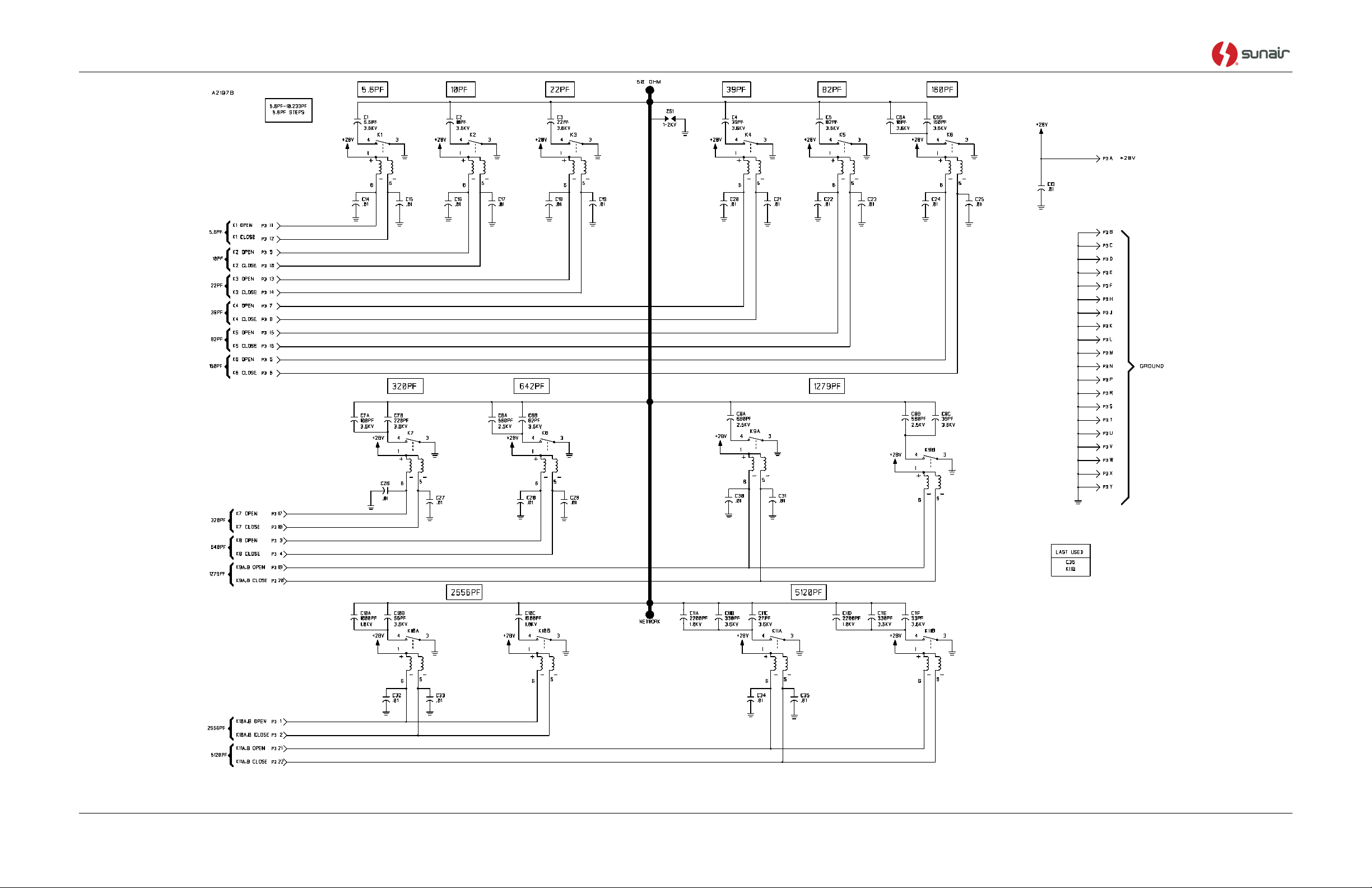
CU-9150
Figure 5.7-8. PC Assembly, Input Capacitor, 1A1A4A2
(Page 2 of 2)
5-36 Use or disclosure of information from this document is subject to the restrictions
indicated on the proprietary/confidentiality page of this document.
Page 85
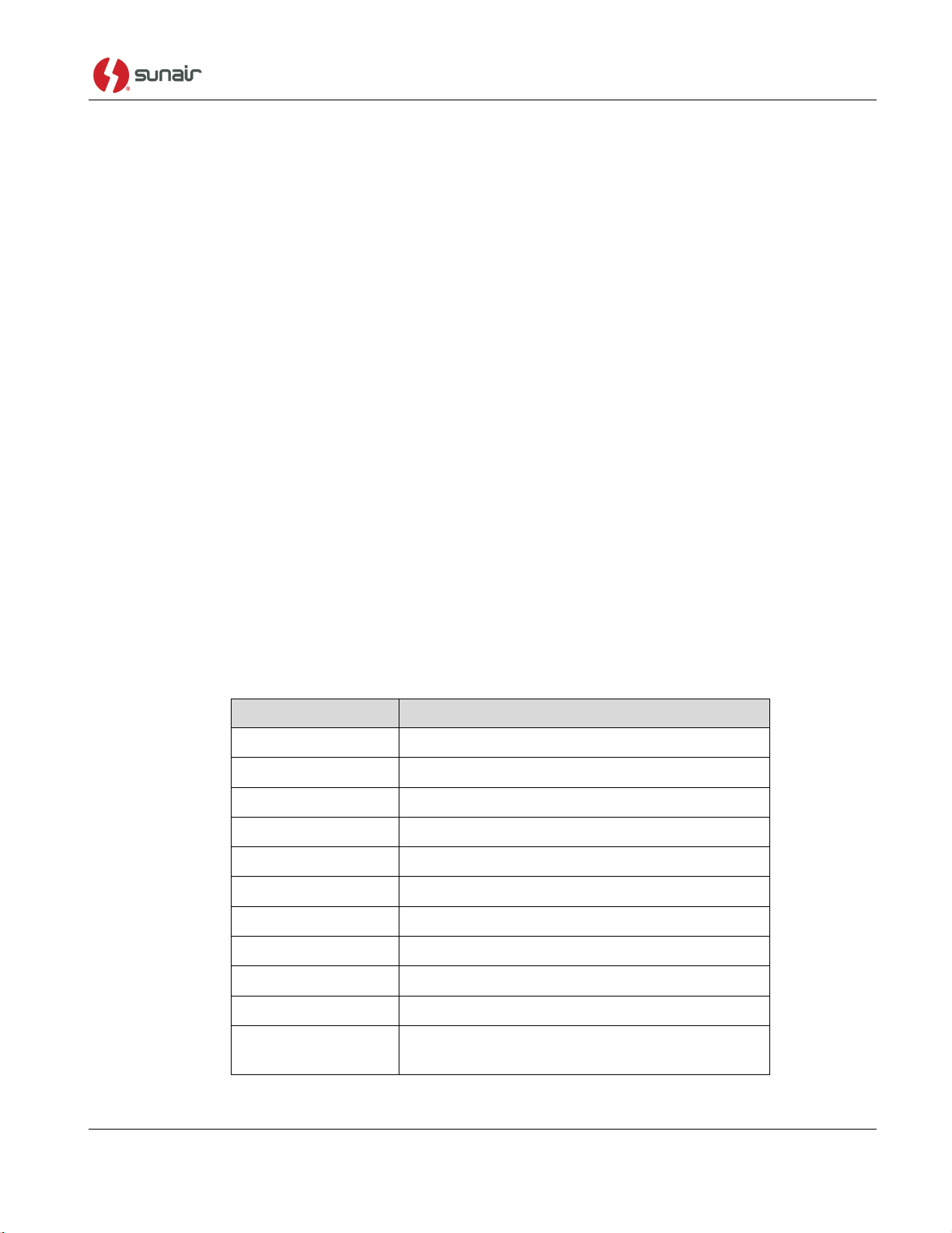
CU-9150
Sunair Part No.
Description
1012890031
Cable Assembly, DB-9 Male to DB-9 Female
1012900037
Cable Assembly, DB-25 Male to DB-9 Female
8092500096
Cable Assembly, LPA-9600 to Coupler
8120030036
Kilowatt Coupler CPU Test Fixture
8120034091
EPROM with Test Fixture Software
8120037189
Software, TuneView, on disk
8120037391
Tested Serial Breakout Board
8120039394
Tested Display Board
8120907604
Carrying Case, Black Plastic
8120907701
Bracket, Panel Support
8120907892
Cable Assembly, CU-9150 to DTS (DB9 Male
to Male)
SECTION VI – Options
6.0 Options
6.1 Diagnostic Test Set
6.1.1 General Information
6.1.1.1 Scope of Option Section
This section contains information necessary to utilize the TS-9150 Diagnostic Test Set to isolate faults
in a CU-9150/CU-9100A Kilowatt Antenna Coupler.
6.1.1.2 Purpose of Equipment
The TS-9150 Diagnostic Test Set provides the tools required to diagnose and isolate faults in a
CU-9150/CU-9100A Kilowatt Antenna Coupler. Three separate functions are provided:
Coupler CPU board level test capability
Display of coupler state and the ability to modify that state
Display of coupler tuning history
6.1.1.3 Equipment Supplied
Table 6.1-1 provides a list of equipment, with appropriate Sunair part numbers, supplied as the TS-9150
Diagnostic Test Set.
Table 6.1-1 Equipment Supplied
Use or disclosure of information from this document is subject to the restrictions 6-1
indicated on the proprietary/confidentiality page of this document.
Page 86
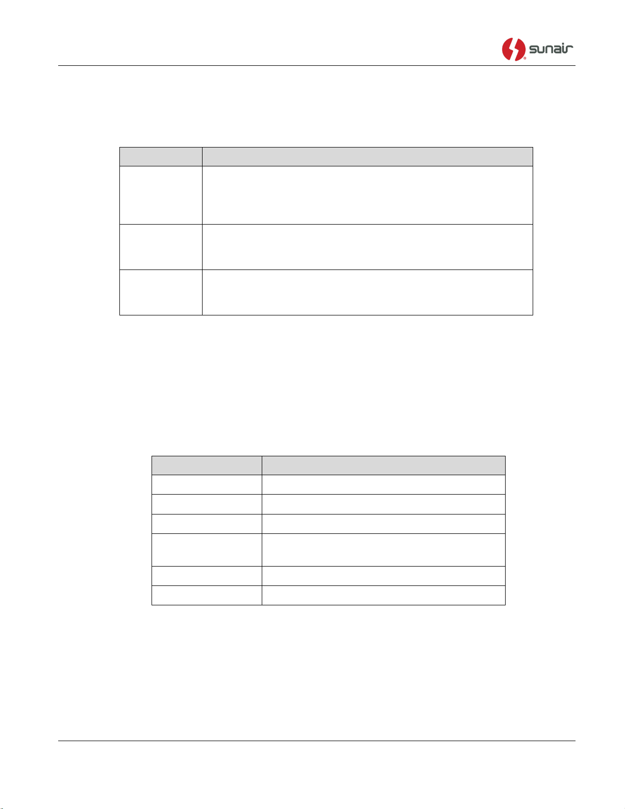
CU-9150
Term
Definition
Network
A combination of input capacitance (Cin), series inductance
(Lseries), output capacitance (Cout), and output inductance
(Lout) which comprise a matching circuit between the antenna
terminal and the RF input connector.
Network
Element
One of the four reactive matching elements. These elements
are Cin, Lseries, Cout, and Lout. Each network element is
made up of many network components.
Network
Component
One of the discrete reactive components in the coupler. For
example, C1 on the Input Capacitor board is a network
component
Sunair Part No.
Description
1012890031
Cable Assy, DB-9 Male to DB-9 Female
8120030036
Kilowatt Coupler CPU Test Fixture
8120034091
EPROM with Test Fixture Software
8120907892
Cable Assy, CU-9150 to DTS (DB9 Male to
Male)
CFE
DC Power Supply, 28V at 2A
CFE
PC or Terminal
The following sections detail the operation of the different functions of the TS-9150. Table 6.1-2
explains the terms as they are used to describe coupler operation.
Table 6.1-2 Coupler Operation Terms
6.1.2 Test Set Operation
6.1.2.1 CPU Test Fixture Operation
In order to perform a board level test of the 8120030095 Coupler CPU assembly, the components listed
in Table 6.1-3 are required. All of the items that have Sunair part numbers are included with the
8120907591 Diagnostic Test Set.
Table 6.1-3. Board Level Test Components Required
To perform a board level test:
1. Remove the EPROM from the U301 position of the board under test.
2. Install the Test EPROM PN 8120034091 in the U301 position.
3. Remove PAL W/CU-9150-H software from U105 position.
4. Install PN 8120033698 PAL W/CU-9150 software in U105 position.
6-2 Use or disclosure of information from this document is subject to the restrictions
indicated on the proprietary/confidentiality page of this document.
Page 87

CU-9150
5. Set S1 on the test fixture to its OFF (down) position.
6. Set all of the switches on S201 of the board under test to the OFF (down) position.
7. Set S601 on the test fixture to RUN EEPROM TEST.
Configure the PC or terminal serial communications parameters for 8 bits, no parity, one stop bit, at
9600 bps. Choose ASCII if more than one character set is supported by the terminal or program. No
special escape codes are utilized by the test software, so most terminal emulation modes will work fine.
VT-100 terminal emulation works well and is supported by most PC terminal programs.
If Hyperterminal is being used in a Windows 95 environment, the communications setup can be
accomplished as follows:
1. Open the Hyperterminal folder by clicking Start in the lower left hand corner, clicking
Accessories, and Hyperterminal.
2. Start Hyperterminal by clicking on the Hypertrm.exe icon.
3. Choose a name for the new “connection” being created. The “connection” is really just a
collection of serial communications parameters which can be stored for later use.
4. Choose an icon for the connection and click OK.
5. On the next dialog box, select the desired COM port under the “Connect using”. Most users will
need to select either Direct to Com 1 or Direct to Com 2. Click OK.
The next dialog box is where the actual communication parameter setup takes place.
6. Set the Bits per second list box to 9600.
7. Set the Data bits list box to 8.
8. Set the Parity list box to None.
9. Set the Stop bits list box to 1.
10. Set the Flow control list box to None.
11. Click OK.
The Hyperterminal main screen now appears, and is ready to display the test fixture output. When the
test session is complete and Hyperterminal is closed, it will ask if the session should be saved. Answer
Yes to this question so that Hyperterminal will save the connection, and create a new icon in the
Hyperterminal folder. In the future, Hyperterminal should be started by clicking on this new icon so that
the communications parameters do not have to be set up for every test session.
1. Connect P1 (TO PC) on the test fixture to the PC or terminal serial port. Plug the CPU to be
tested into the fixture. Note that the component side the board should be facing the front of the
fixture. The front of the fixture is labeled FRONT OF BOARD. This is important, as it is
possible to plug the CPU into the fixture backwards.
CAUTION Carefully observe the orientation of the board under test with respect to the test
fixture. Make sure that the component side of the board under test faces toward
the front of the test fixture (labeled FRONT OF BOARD). Failure to do so can
result in damage to the fixture and the board under test.
Use or disclosure of information from this document is subject to the restrictions 6-3
indicated on the proprietary/confidentiality page of this document.
Page 88

CU-9150
2. Connect P2 (TO BOARD UNDER TEST) to J1 of the CPU assembly being tested using cable
PN 8120907892.
3. Set the power supply output voltage to 28V. Turn the power supply off and connect it to J3 on
the test fixture.
4. Turn on the power supply.
5. Turn on the fixture power supply using S1.
6. Follow the instructions that appear on the terminal screen.
If the board under test is good, the last line displayed on the terminal at the completion of the test will be
PASSED. Otherwise FAILED will be displayed.
When a test fails, a message describing the failure will be displayed on the terminal and the program
will not continue until the CONTINUE button is pressed on the test fixture.
To restart the test, press the reset switch (S101) on the board under test.
Since the EEPROM test takes quite a while to complete, it can be bypassed during troubleshooting by
setting S602 on the test fixture to BYPASS EEPROM TEST and pressing the reset switch (S101 on the
board under test). In this case, the program will always display *** TEST FAILED *** at the end of the
test.
At the end of the test, all four LEDs at the top of the board under test should be lighting in sequence.
Before installing the CPU board back in a coupler, remove the test EPROM and put the standard
EPROM PN 8120033299 back into the U301 position.
Remove PN 8120033698 from U105 position and reinstall PN 8120810198 into position U105.
6.1.2.2 Display Board Operation
The display board allows the user to view and modify the state of the relays in the coupler. The display
board is little more than a collection of displays and switches that can be addressed serially by the
coupler CPU. The display board occupies the right side of the Diagnostic Test Set case.
In order for the display board to be utilized, DIP switch number 7 of S201 on the coupler CPU must be
in the UP (ON) position. However, with the switch in this position, the CPU clock is active at all times,
and is easily heard by the radio receiver. For this reason, DIP switch number 7 of S201 should only be
in the UP position during coupler diagnostics, and should be in the DOWN position during normal
operation.
Turn the radio set off. Remove the coupler cover. Remove the inner cover. Set DIP switch number 7 of
S201 on the coupler CPU to its UP position. Connect cable PN 8120907892 (DB9 Male to Male)
between J1 of the CPU board (labeled DISPLAY on the inner cover) and J1 on the display board (labeled
TO COUPLER CPU). Set the ON/OFF switch on the display board to ON. Turn the radio set on.
The display board now indicates the state of each relay in the coupler. It also shows the sum total
capacitance or inductance values for each of the network elements.
6-4 Use or disclosure of information from this document is subject to the restrictions
indicated on the proprietary/confidentiality page of this document.
Page 89

CU-9150
At this point, the value of any network element can be modified by pressing the up or down buttons for
that element. For instance, pressing C IN UP will add one increment of capacitance (about 5 pF) to the
amount of Cin that is already active. Pressing the C IN UP button and holding it down will cause
capacitance to be added to Cin continuously. The buttons for Lseries, Cout, and Lout work in a similar
manner.
The red LEDs for each network component correspond to a relay. When a LED is lit, it indicates that
the component associated with that relay is in use in the network. If the component is a capacitor, then
the relay is closed. If the component is an inductor, then the relay is open unless it is the Lout bypass
relay. The Lout bypass relays (K15 and K19 on the chassis) are in the bypass state (connected to the
Normally Closed contact) when the LOUT BYPASS LED is illuminated.
The HOME button causes the coupler to go to a state in which all network elements are 0 pf or 0 µH.
The TUNE/KW button causes the coupler to switch the state of the RF detector. When the red TUNE
LED is lit, the detector is switched into the RF path and the readings from the magnitude and phase
detectors are displayed on the display board.
CAUTION Never apply more than tune power to the coupler when the red
TUNE LED is lit on the display board. Tune power is AM carrier
power and is roughly 40 watts. Higher power levels will destroy
the RF detector components.
A network solution can be arrived at by hand when the red TUNE LED is lit, and AM carrier power is
applied by keying the radio in AM mode (with the LPA-9600 kilowatt amplifier turned off). When the
magnitude and phase displays are as close to zero as possible, then the coupler is tuned.
The magnitude and phase displays show the magnitude and phase detector output values in millivolts.
When the green KW LED is lit, the RF detector is switched out of the RF path. The magnitude and
phase detectors are no longer active, so the display board simply indicates “-----” on the magnitude and
phase displays. It is safe to transmit at the 1000 watt power level in this state.
The SAVE and RECALL keys work in conjunction with the CHANNEL indicator on the display board.
Note that the channel indicator does not indicate the channel the radio is on. The channel indicator
provides access to the coupler channel memory. To save a network solution for later use, dial in a
channel number using the knobs below the channel indicator and press the SAVE button. This will save
the network in that channel location in the coupler’s memory. The network solution can be recalled at a
later time in two ways. The first method is to set the radio to the desired channel number. The other
method is to use the knobs below the channel indicator to dial in the desired channel, and then press the
RECALL button.
The CPU TUNE START and CPU TUNE STEP keys are reserved for future use and are disabled.
6.1.2.3 Serial Breakout Board Operation
The Serial Breakout Board provides the user with the ability to see the steps the coupler took in arriving
at a network solution. The Serial Breakout Board is installed on the left side of the Diagnostic Test Set
case.
Table 6.1-4 lists the equipment to use the Serial Breakout section of the test set.
Use or disclosure of information from this document is subject to the restrictions 6-5
indicated on the proprietary/confidentiality page of this document.
Page 90
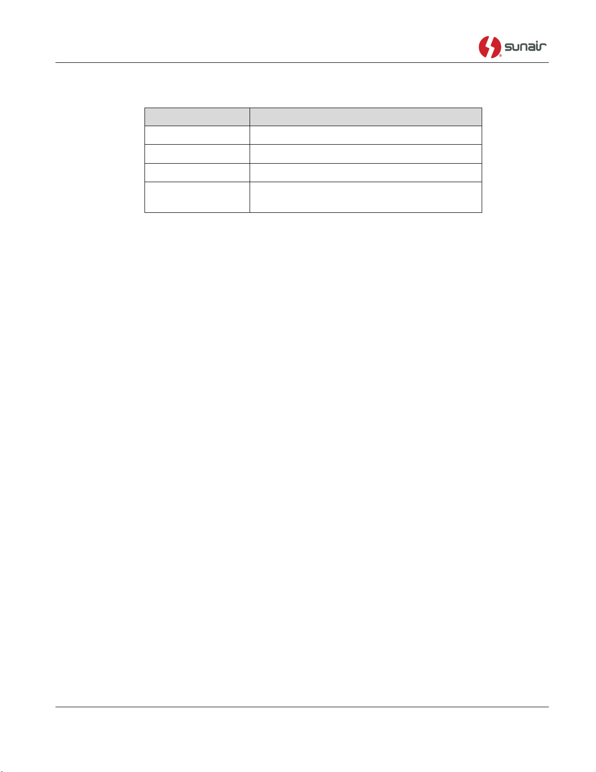
CU-9150
Sunair Part No.
Description
1012900037
Cable Assy, DB25 Male to DB9 Female
8092500096
Cable Assy, LPA-9600 to Coupler
8120037189
Software, TuneView
CFE
PC running Windows 3.1 or later with an
available serial port
Table 6.1-4 Serial Breakout Equipment Required
This list assumes that there is an existing cable between the LPA-9600/LPA-9500 and the antenna
coupler.
The TuneView software can be run directly from the distribution floppy, but it is preferable to have it
resident on the hard drive. To install TuneView:
1. Insert the TuneView diskette into the floppy drive
2. Open a DOS window
3. Create a new directory ( md\TuneView )
4. Change to that directory ( cd\TuneView )
5. Copy the TuneView executable ( copy a:TuneView.exe . )
6. Close the DOS window ( exit )
7. Create a shortcut to the TuneView executable on the desktop.
Disconnect the control cable between the linear amplifier and the coupler at the amplifier end (J4 on the
amplifier rear panel). Connect this cable to J2 on the Diagnostic Test Set (labeled TO KILOWATT
COUPLER). Connect the other control cable (PN 8092500096) between J1 of the Diagnostic Test Set
and J4 of the amplifier. Using the DB25 to DB9 cable PN 1012900037, connect the 25-pin end to J5 of
the Diagnostic Test Set Serial Breakout Board. Connect the other end to the serial port of the PC
running TuneView.
Start TuneView. The first time TuneView is run, it must be configured to use the COM port connected
to the Serial Breakout Board. On the menu, click on Settings, and then on Com Port. This will bring
up a dialog box that allows selection of the desired COM port. This information is stored on disk so that
the correct COM port is selected the next time TuneView is run.
The TuneView main screen displays several parameters describing the most recent tune. These are listed
in Table 6.1-5.
The magnitude and phase values for each network are plotted on the chart as a small red square. The
center of the chart is magnitude=0 mV, phase=0 mV. This corresponds to a network input impedance of
50 ohms at 0 degrees. Positive phase values are plotted in the top half of the chart. Negative magnitude
values are plotted on the right hand side of the chart. This is because the magnitude detector output is
negative for impedances which have a magnitude greater than 50 ohms, and positive for impedances
6-6 Use or disclosure of information from this document is subject to the restrictions
indicated on the proprietary/confidentiality page of this document.
Page 91
CU-9150
Term
Definition
Channel
The radio channel that was tuned.
Freq
The radio frequency that was tuned. This frequency is truncated to display
megahertz only. For example, if the radio frequency was 6.99999 MHz,
TuneView would show 6 under Freq.
Magoffset
The output of the magnitude detector in millivolts when the 50 ohm calibration
load is switched in. This number is subtracted from all future readings of the
detector, so minor detector imbalances over time, temperature, and frequency
do not affect the network solution. If this number is greater than 250 or less than
-250, the RF detector board should be adjusted to null the magnitude detector.
Phaseoffset
The output of the phase detector in millivolts when the 50 ohm calibration load is
switched in. This number is subtracted from all future readings of the detector,
so minor detector imbalances over time, temperature, and frequency do not
affect the network solution. If this number is greater than 250 or less than -250,
the RF detector board should be adjusted to null the phase detector.
Network #
This is the number of the attempt by the coupler to arrive at a network solution.
Each network consists of a value of Cin, Lseries, Cout, and Lout. The
magnitude and phase readings corresponding to this network are also displayed.
The larger the network number, the later in the tune cycle that it occurred.
Cin
The input capacitance of the currently selected network. Each bit in the top
number corresponds to a relay. If the bit is 1, then the corresponding relay is
closed, making its associated Cin component active in the network. The bottom
number is Cin in picofarads.
Lseries
The series inductance of the currently selected network. Each bit in the top
number corresponds to a relay. If the bit is 1, then the corresponding relay is
open, making its associated Lseries component active in the network. The
bottom number is Lseries in microhenrys.
Cout
The output capacitance of the currently selected network. Each bit in the top
number corresponds to a relay. If the bit is 1, then the corresponding relay is
closed, making its associated Cout component active in the network. The
bottom number is Cout in picofarads.
Lout
The output inductance of the currently selected network. If the bit is 1, then the
corresponding relay is open, making its associated Lout component active in the
network. The bottom number is Lout in microhenrys. If lout=0, then the Lout
bypass relays (K15 and K19 on the chassis) are in the bypass state (connected
to the Normally Closed contact).
which have a magnitude less than 50 ohms. Using this convention, the plot produced is similar to a
Smith chart.
Table 6.1-5. TuneView Parameters
The arrow keys control which network is displayed. The currently selected network is shown on the
chart as the single blue square. All of the other attempts are shown as red squares. Pressing the UP
Use or disclosure of information from this document is subject to the restrictions 6-7
indicated on the proprietary/confidentiality page of this document.
Page 92

CU-9150
ARROW key moves to networks earlier in the tune cycle. Pressing the DOWN ARROW key moves to
networks later in the tune cycle.
The PAGE UP key performs the same function as the UP ARROW key. The PAGE DOWN key
performs the same function as the DOWN ARROW key.
The box at the bottom of the screen shows a log of the tuning attempts for the current session. For each
tune attempt, a line is added showing the channel number and whether or not the tune was successful.
The currently displayed tune history can be saved to a file using the menu item File, and then Save As.
This file can later be loaded by clicking File, then Open, and selecting the desired file.
6.1.2.4 BITE
The built in test function (BITE) of the coupler is initiated under the BITE menu on the radio, by the
CU-BITE softkey. Pressing CU-BITE causes the radio to tune the coupler on four dedicated BITE
channels, shown below:
Channel Frequency
250 1.75 MHz
251 5.75 MHz
252 16.75 MHz
253 29.75 MHz
The coupler is aware that a BITE test should be performed because these channels are only used for
BITE.
After a tune solution is found, but before sending a READY signal back to the radio, the coupler checks
a portion of the relays. This check consists of changing the state of each relay, one at a time, and
determining if this change makes a sufficient difference in the readings of the magnitude and phase
detectors.
If the coupler does not detect a large enough change in the magnitude and phase detector readings as it
changes the state of each relay, it reports a tuning FAULT signal back to the radio. If the coupler does
detect a large enough change in the magnitude and phase detector readings, it reports a READY signal
back to the radio.
When a CU-BITE failure occurs, it is necessary to use TuneView and the Serial Breakout Board to find
out which components the coupler determined to be faulty. Connect the Serial Breakout Board and start
TuneView as detailed in Section 6.1.2.3. Run the CU-BITE test again. The list box at the bottom of the
TuneView screen will indicate which components need attention.
The list box also contains information about each relay check. The state of all of the relays in shown
along with the magnitude and phase difference that was generated by toggling the state of one relay.
The small value components are not checked individually. Rather, the three smallest Cin values (C1,
C2, and C3 on the Input Capacitor board) are checked as a group and the three smallest Lseries values
(L9, L1, and L2 on the chassis) are checked as a group. The coupler switches the three smallest Cin
components out of the network and takes a magnitude and phase reading. It then switches the three
smallest components into the network and takes another magnitude and phase reading. As long as these
two readings have a large enough difference between them, all of the components in the group are
assumed to be working properly. The three smallest Lseries values are checked in the same way.
6-8 Use or disclosure of information from this document is subject to the restrictions
indicated on the proprietary/confidentiality page of this document.
Page 93
CU-9150
PC ASSEMBLY, TEST FIXTURE, CU-9150 CPU
TEST FIXTURE, CU-9150 CPU
8120030036
C1
CAP. 0.01UF, 50V, X7R, 20%
0281730008
C2
CAP. 22UF, 15V
0281690006
C3
CAP. 22UF, 15V
0281690006
C4
CAP. 47UF, 20V
0281700001
C5
CAP. 10UF, 20V
1007290005
C6
CAP. 47UF, 20V
0281700001
C7
CAP. 0.01UF, 50V, X7R, 20%
0281730008
C8
CAP. 1UF, 35V
0281660000
C9
CAP. 0.1UF, 50V, X7R
1011180014
C10
CAP. 0.01UF, 50V, X7R, 20%
0281730008
C11
CAP. 0.01UF, 50V, X7R, 20%
0281730008
C12
CAP. 0.1UF, 50V, X7R
1011180014
C13
CAP. 68UF, 15V
0296540005
C201
CAP. 0.01UF, 50V, X7R, 20%
0281730008
C202
CAP. 0.01UF, 50V, X7R, 20%
0281730008
C203
CAP. 0.01UF, 50V, X7R, 20%
0281730008
C309
CAP. 0.01UF, 50V, X7R, 20%
0281730008
C310
CAP. 0.01UF, 50V, X7R, 20%
0281730008
C401
CAP. 0.01UF, 50V, X7R, 20%
0281730008
C402
CAP. 0.01UF, 50V, X7R, 20%
0281730008
C403
CAP. 0.01UF, 50V, X7R, 20%
0281730008
C404
CAP. 0.01UF, 50V, X7R, 20%
0281730008
C501
CAP. 0.01UF, 50V, X7R, 20%
0281730008
C502
CAP. 0.01UF, 50V, X7R, 20%
0281730008
C601
CAP. 0.01UF, 50V, X7R, 20%
0281730008
C602
CAP. 0.01UF, 50V, X7R, 20%
0281730008
C603
CAP. 0.01UF, 50V, X7R, 20%
0281730008
C604
CAP. 0.01UF, 50V, X7R, 20%
0281730008
CR1
DIODE, LED, RED MV5754A
1004350023
CR2
DIODE, RECTIFIER 1N4004
0405180004
CR3
DIODE, RECTIFIER 1N4004
0405180004
F1
FUSE, MDL, 3 AMP, 32V
0896660001
J1
CONNECTOR, PCB, 100 PIN
1013190025
J2
CONNECTOR, DB-9, FEMALE RT ANG
1012550028
J3
CONNECTOR, PC, 2 PIN HEADER
1008060011
K201
RELAY, PHOTOMOS, 40V,2A
1012550036
K202
RELAY, PHOTOMOS, 40V,2A
1012550036
K203
RELAY, PHOTOMOS, 40V,2A
1012550036
K204
RELAY, PHOTOMOS, 40V,2A
1012550036
K205
RELAY, PHOTOMOS, 40V,2A
1012550036
K206
RELAY, PHOTOMOS, 40V,2A
1012550036
K207
RELAY, PHOTOMOS, 40V,2A
1012550036
K208
RELAY, PHOTOMOS, 40V,2A
1012550036
K209
RELAY, PHOTOMOS, 40V,2A
1012550036
K210
RELAY, PHOTOMOS, 40V,2A
1012550036
K211
RELAY, PHOTOMOS, 40V,2A
1012550036
K212
RELAY, PHOTOMOS, 40V,2A
1012550036
K213
RELAY, PHOTOMOS, 40V,2A
1012550036
K214
RELAY, PHOTOMOS, 40V,2A
1012550036
K215
RELAY, PHOTOMOS, 40V,2A
1012550036
K216
RELAY, PHOTOMOS, 40V,2A
1012550036
K301
RELAY, PHOTOMOS, 40V,2A
1012550036
K302
RELAY, PHOTOMOS, 40V,2A
1012550036
K303
RELAY, PHOTOMOS, 40V,2A
1012550036
K304
RELAY, PHOTOMOS, 40V,2A
1012550036
K305
RELAY, PHOTOMOS, 40V,2A
1012550036
K306
RELAY, PHOTOMOS, 40V,2A
1012550036
K307
RELAY, PHOTOMOS, 40V,2A
1012550036
K308
RELAY, PHOTOMOS, 40V,2A
1012550036
K309
RELAY, PHOTOMOS, 40V,2A
1012550036
K310
RELAY, PHOTOMOS, 40V,2A
1012550036
K311
RELAY, PHOTOMOS, 40V,2A
1012550036
K312
RELAY, PHOTOMOS, 40V,2A
1012550036
K313
RELAY, PHOTOMOS, 40V,2A
1012550036
K314
RELAY, PHOTOMOS, 40V,2A
1012550036
K315
RELAY, PHOTOMOS, 40V,2A
1012550036
K316
RELAY, PHOTOMOS, 40V,2A
1012550036
K401
RELAY, PHOTOMOS, 40V,2A
1012550036
K402
RELAY, PHOTOMOS, 40V,2A
1012550036
K403
RELAY, PHOTOMOS, 40V,2A
1012550036
K404
RELAY, PHOTOMOS, 40V,2A
1012550036
K405
RELAY, PHOTOMOS, 40V,2A
1012550036
K406
RELAY, PHOTOMOS, 40V,2A
1012550036
K407
RELAY, PHOTOMOS, 40V,2A
1012550036
K408
RELAY, PHOTOMOS, 40V,2A
1012550036
K409
RELAY, PHOTOMOS, 40V,2A
1012550036
K410
RELAY, PHOTOMOS, 40V,2A
1012550036
K411
RELAY, PHOTOMOS, 40V,2A
1012550036
K412
RELAY, PHOTOMOS, 40V,2A
1012550036
K413
RELAY, PHOTOMOS, 40V,2A
1012550036
K414
RELAY, PHOTOMOS, 40V,2A
1012550036
K415
RELAY, PHOTOMOS, 40V,2A
1012550036
K416
RELAY, PHOTOMOS, 40V,2A
1012550036
K417
RELAY, PHOTOMOS, 40V,2A
1012550036
K418
RELAY, PHOTOMOS, 40V,2A
1012550036
K419
RELAY, PHOTOMOS, 40V,2A
1012550036
K420
RELAY, PHOTOMOS, 40V,2A
1012550036
K421
RELAY, PHOTOMOS, 40V,2A
1012550036
K422
RELAY, PHOTOMOS, 40V,2A
1012550036
K423
RELAY, PHOTOMOS, 40V,2A
1012550036
K424
RELAY, PHOTOMOS, 40V,2A
1012550036
K501
RELAY, PHOTOMOS, 40V,2A
1012550036
K502
RELAY, PHOTOMOS, 40V,2A
1012550036
K503
RELAY, PHOTOMOS, 40V,2A
1012550036
K504
RELAY, PHOTOMOS, 40V,2A
1012550036
K505
RELAY, PHOTOMOS, 40V,2A
1012550036
K506
RELAY, PHOTOMOS, 40V,2A
1012550036
K507
RELAY, PHOTOMOS, 40V,2A
1012550036
K508
RELAY, PHOTOMOS, 40V,2A
1012550036
K601
RELAY, PHOTOMOS, 40V,2A
1012550036
K602
RELAY, PHOTOMOS, 40V,2A
1012550036
K603
RELAY, PHOTOMOS, 40V,2A
1012550036
K604
RELAY, PHOTOMOS, 40V,2A
1012550036
K605
RELAY, PHOTOMOS, 40V,2A
1012550036
K606
RELAY, PHOTOMOS, 40V,2A
1012550036
K607
RELAY, PHOTOMOS, 40V,2A
1012550036
K608
RELAY, PHOTOMOS, 40V,2A
1012550036
P1
CONNECTOR, DB-9, FEMALE RT ANG
1012550028
R1
RESISTOR 4.7K, 5%, 1/4W
0170770001
R2
RESISTOR 1K, 5%, 1/8W
1010801023
R3
RESISTOR 27K, 5%, 1/8W
1010802739
R4
RESISTOR 27K, 5%, 1/8W
1010802739
R5
RESISTOR 2.2K, 5%, 1/8W
1010802224
R6
RESISTOR 22K, 5%, 1/8W
1010802232
R7
RESISTOR 3.9K, 5%, 1/8W
1010803921
R201
RESISTOR 680, 5%, 1/8W
1010806815
R202
RESISTOR 680, 5%, 1/8W
1010806815
R203
RESISTOR 680, 5%, 1/8W
1010806815
R204
RESISTOR 680, 5%, 1/8W
1010806815
R205
RESISTOR 680, 5%, 1/8W
1010806815
R206
RESISTOR 680, 5%, 1/8W
1010806815
R207
RESISTOR 680, 5%, 1/8W
1010806815
R208
RESISTOR 680, 5%, 1/8W
1010806815
R209
RESISTOR 680, 5%, 1/8W
1010806815
R210
RESISTOR 680, 5%, 1/8W
1010806815
R211
RESISTOR 680, 5%, 1/8W
1010806815
R212
RESISTOR 680, 5%, 1/8W
1010806815
R213
RESISTOR 680, 5%, 1/8W
1010806815
R214
RESISTOR 680, 5%, 1/8W
1010806815
R215
RESISTOR 680, 5%, 1/8W
1010806815
R216
RESISTOR 680, 5%, 1/8W
1010806815
R217
RESISTOR 470, 10%, 2W
0163580006
R218
RESISTOR 10K, 5%, 1/8W
1010801031
Use or disclosure of information from this document is subject to the restrictions 6-9
indicated on the proprietary/confidentiality page of this document.
Figure 6.1-1. PC Assembly, Test Fixture, CU-9150 CPU
(Page 1 of 9)
Page 94
CU-9150
PC ASSEMBLY, TEST FIXTURE, CU-9150 CPU (Continued)
R219
RESISTOR10K, 5%, 1/8W
1010801031
R220
RESISTOR470, 10%,2W
0163580006
R221
RESISTOR470, 10%,2W
0163580006
R222
RESISTOR470, 10%,2W
0163580006
R223
RESISTOR470, 10%,2W
0163580006
R224
RESISTOR470, 10%,2W
0163580006
R225
RESISTOR470, 10%,2W
0163580006
R301
RESISTOR680, 5%, 1/8W
1010806815
R302
RESISTOR680, 5%, 1/8W
1010806815
R303
RESISTOR680, 5%, 1/8W
1010806815
R304
RESISTOR680, 5%, 1/8W
1010806815
R305
RESISTOR680, 5%, 1/8W
1010806815
R306
RESISTOR680, 5%, 1/8W
1010806815
R307
RESISTOR680, 5%, 1/8W
1010806815
R308
RESISTOR680, 5%, 1/8W
1010806815
R309
RESISTOR680, 5%, 1/8W
1010806815
R310
RESISTOR680, 5%, 1/8W
1010806815
R311
RESISTOR680, 5%, 1/8W
1010806815
R312
RESISTOR680, 5%, 1/8W
1010806815
R313
RESISTOR680, 5%, 1/8W
1010806815
R314
RESISTOR680, 5%, 1/8W
1010806815
R315
RESISTOR680, 5%, 1/8W
1010806815
R316
RESISTOR680, 5%, 1/8W
1010806815
R401
RESISTOR680, 5%, 1/8W
1010806815
R402
RESISTOR680, 5%, 1/8W
1010806815
R403
RESISTOR680, 5%, 1/8W
1010806815
R404
RESISTOR680, 5%, 1/8W
1010806815
R405
RESISTOR680, 5%, 1/8W
1010806815
R406
RESISTOR680, 5%, 1/8W
1010806815
R407
RESISTOR680, 5%, 1/8W
1010806815
R408
RESISTOR680, 5%, 1/8W
1010806815
R409
RESISTOR680, 5%, 1/8W
1010806815
R410
RESISTOR680, 5%, 1/8W
1010806815
R411
RESISTOR680, 5%, 1/8W
1010806815
R412
RESISTOR680, 5%, 1/8W
1010806815
R413
RESISTOR680, 5%, 1/8W
1010806815
R414
RESISTOR680, 5%, 1/8W
1010806815
R415
RESISTOR680, 5%, 1/8W
1010806815
R416
RESISTOR680, 5%, 1/8W
1010806815
R417
RESISTOR680, 5%, 1/8W
1010806815
R418
RESISTOR680, 5%, 1/8W
1010806815
R419
RESISTOR680, 5%, 1/8W
1010806815
R420
RESISTOR680, 5%, 1/8W
1010806815
R421
RESISTOR 680, 5%, 1/8W
1010806815
R422
RESISTOR 680, 5%, 1/8W
1010806815
R423
RESISTOR 680, 5%, 1/8W
1010806815
R424
RESISTOR 680, 5%, 1/8W
1010806815
R425
RESISTOR 470, 10%, 2W
0163580006
R426
RESISTOR 10K, 5%, 1/8W
1010801031
R427
RESISTOR 10K, 5%, 1/8W
1010801031
R428
RESISTOR 470, 10%, 2W
0163580006
R429
RESISTOR 470, 10%, 2W
0163580006
R501
RESISTOR 680, 5%, 1/8W
1010806815
R502
RESISTOR 680, 5%, 1/8W
1010806815
R503
RESISTOR 680, 5%, 1/8W
1010806815
R504
RESISTOR 680, 5%, 1/8W
1010806815
R505
RESISTOR 680, 5%, 1/8W
1010806815
R506
RESISTOR 680, 5%, 1/8W
1010806815
R507
RESISTOR 680, 5%, 1/8W
1010806815
R508
RESISTOR 680, 5%, 1/8W
1010806815
R509
RESISTOR 680, 5%, 1/8W
1010806815
R510
RESISTOR 680, 5%, 1/8W
1010806815
R511
RESISTOR 680, 5%, 1/8W
1010806815
R512
RESISTOR 680, 5%, 1/8W
1010806815
R513
RESISTOR 680, 5%, 1/8W
1010806815
R514
RESISTOR 680, 5%, 1/8W
1010806815
R515
RESISTOR 680, 5%, 1/8W
1010806815
R516
RESISTOR 680, 5%, 1/8W
1010806815
R517
RESISTOR 10K, 5%, 1/8W
1010801031
R518
RESISTOR 10K, 5%, 1/8W
1010801031
R519
RESISTOR 10K, 5%, 1/8W
1010801031
R520
RESISTOR 10K, 5%, 1/8W
1010801031
R601
RESISTOR 680, 5%, 1/8W
1010806815
R602
RESISTOR 680, 5%, 1/8W
1010806815
R603
RESISTOR 680, 5%, 1/8W
1010806815
R604
RESISTOR 680, 5%, 1/8W
1010806815
R605
RESISTOR 680, 5%, 1/8W
1010806815
R606
RESISTOR 680, 5%, 1/8W
1010806815
R607
RESISTOR 680, 5%, 1/8W
1010806815
R608
RESISTOR 680, 5%, 1/8W
1010806815
R609
RESISTOR 1.8K, 5%, 1/8W
1010801821
R610
RESISTOR 1K, 5%, 1/8W
1010801023
R611
RESISTOR 5.6K, 5%, 1/8W
1010805622
R612
RESISTOR 1K, 5%, 1/8W
1010801023
R613
RESISTOR 1K, 5%, 1/8W
1010801023
R614
RESISTOR 0.0, 0%, 1/4W
1011600021
R615
RESISTOR 0.0, 0%, 1/4W
1011600021
R616
RESISTOR 0.0, 0%, 1/4W
1011600021
R617
RESISTOR 0.0, 0%, 1/4W
1011600021
R618
RESISTOR 0.0, 0%, 1/4W
1011600021
R619
RESISTOR 0.0, 0%, 1/4W
1011600021
R620
RESISTOR 0.0, 0%, 1/4W
1011600021
R621
RESISTOR 0.0, 0%, 1/4W
1011600021
R622
RESISTOR 0.0, 0%, 1/4W
1011600021
R623
RESISTOR 4.7K, 5%, 1/8W
1010804723
R624
RESISTOR 4.7K, 5%, 1/8W
1010804723
S116
SWITCH, TOGGLE, SPDT
1011790033
S601
SWITCH, TOGGLE, SPDT
1011790033
S602
SWITCH, PUSH BUTTON, SQUARE
1013270029
U1
IC DIGITAL, MAX 490
1013240022
U2
IC. DIGITAL, ICL232
1010510011
U201
IC,DIGITAL, UCN5842A
1012530035
U202
IC,DIGITAL, UCN5842A
1012530035
U203
IC. LINEAR, LM2903
1011410036
U301
IC,DIGITAL, UCN5842A
1012530035
U302
IC,DIGITAL, UCN5842A
1012530035
U401
IC. LINEAR, LM2903
1011410036
U402
IC,DIGITAL, UCN5842A
1012530035
U403
IC,DIGITAL, UCN5842A
1012530035
U404
IC,DIGITAL, UCN5842A
1012530035
U501
IC,DIGITAL, UCN5842A
1012530035
U502
IC,DIGITAL, UCN5842A
1012530035
U601
IC,DIGITAL, UCN5842A
1012530035
U602
IC DIGITAL 74HC589
1013250028
U603
IC DIGITAL 74HC589
1013250028
U604
IC. DIGITAL 74HC04
1010280023
U606
IC. LINEAR LM340T5
0448600005
XJ3
CONNECTOR, BLOCK, 2 PIN FEM
1008060038
FUSECLIP, PC MOUNT
0534610005
BACKPLANE, CU-9150 CPU FIXTURE
8120031806
EPROM W/CU9150 CPU TF
SOFTWARE
8120034091
Figure 6.1-1. PC Assembly, Test Fixture, CU-9150 CPU
(Page 2 of 9)
6-10 Use or disclosure of information from this document is subject to the restrictions
indicated on the proprietary/confidentiality page of this document.
Page 95
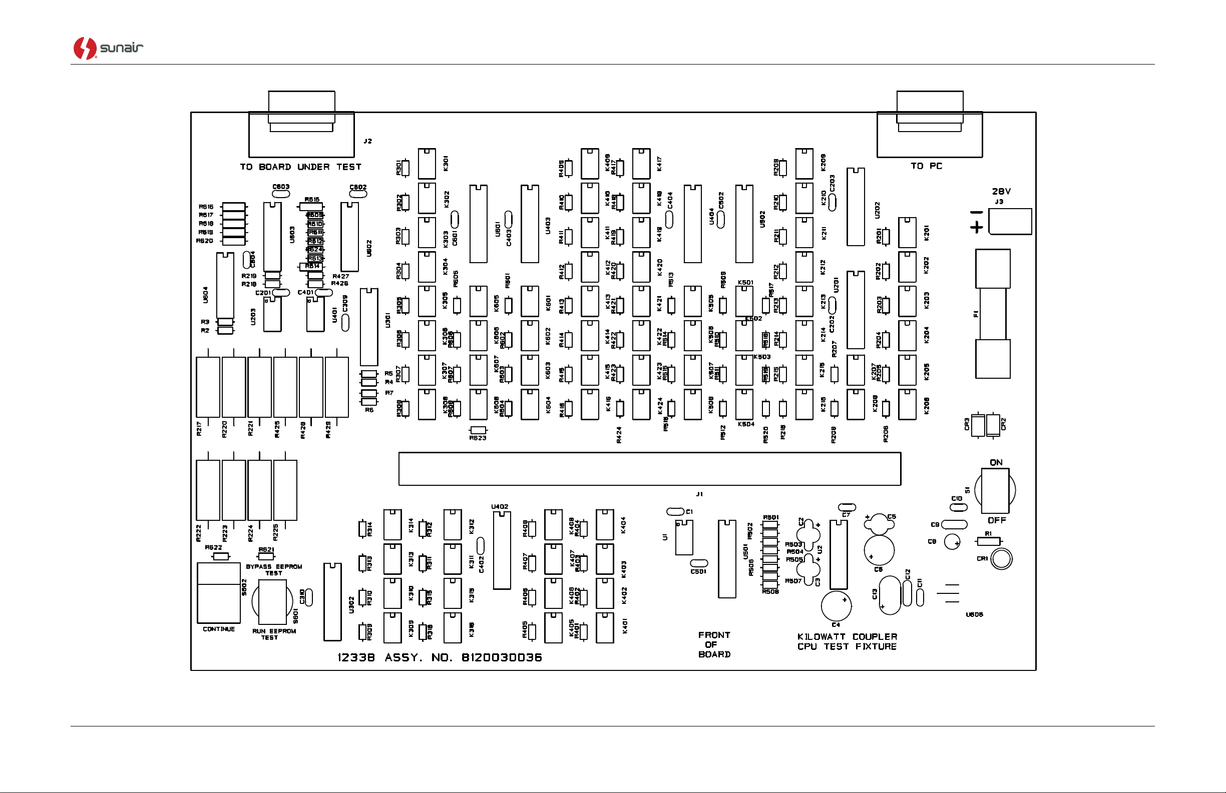
CU-9150
Figure 6.1-1. PC Assembly, Test Fixture, CU-9150 CPU
(Page 3 of 9)
Use or disclosure of information from this document is subject to the restrictions 6-11
indicated on the proprietary/confidentiality page of this document.
Page 96
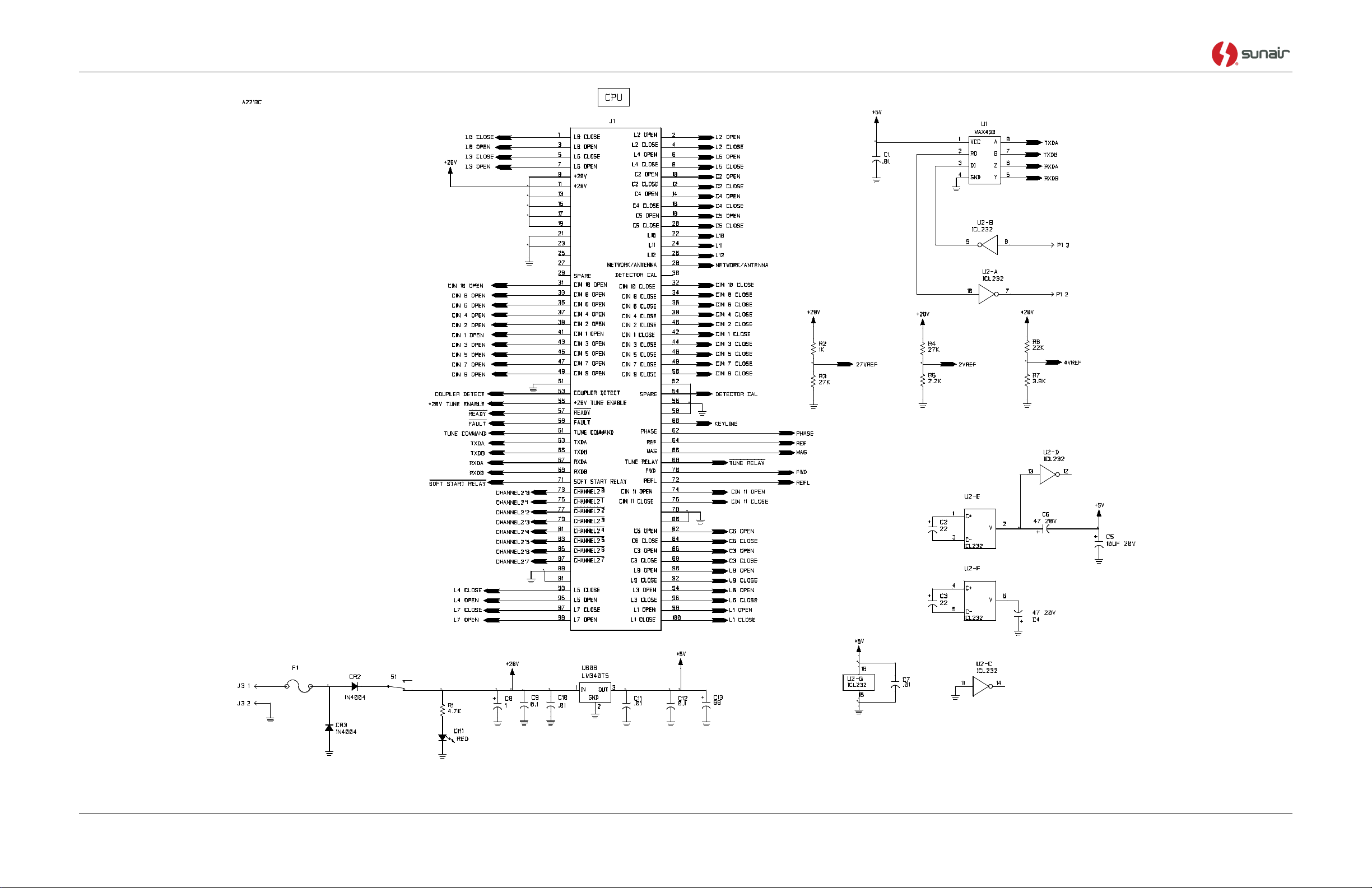
CU-9150
Figure 6.1-1. PC Assembly, Test Fixture, CU-9150 CPU
(Page 4 of 9)
6-12 Use or disclosure of information from this document is subject to the restrictions
indicated on the proprietary/confidentiality page of this document.
Page 97
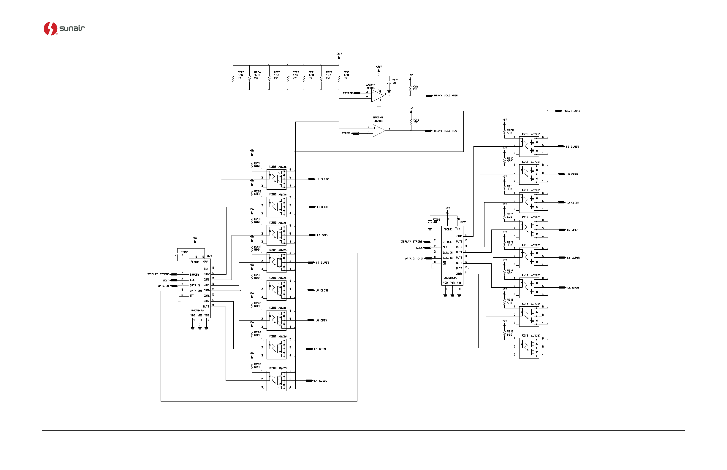
CU-9150
Figure 6.1-1. PC Assembly, Test Fixture, CU-9150 CPU
(Page 5 of 9)
Use or disclosure of information from this document is subject to the restrictions 6-13
indicated on the proprietary/confidentiality page of this document.
Page 98
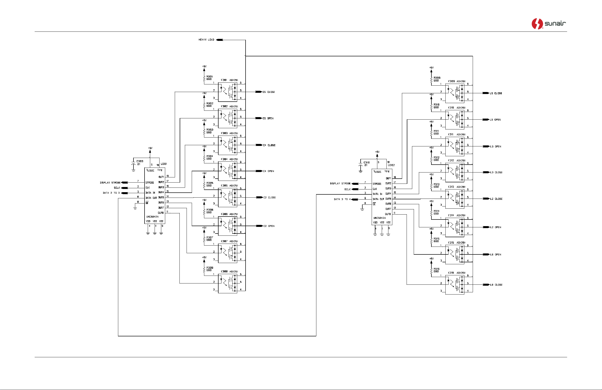
CU-9150
Figure 6.1-1. PC Assembly, Test Fixture, CU-9150 CPU
(Page 6 of 9)
6-14 Use or disclosure of information from this document is subject to the restrictions
indicated on the proprietary/confidentiality page of this document.
Page 99
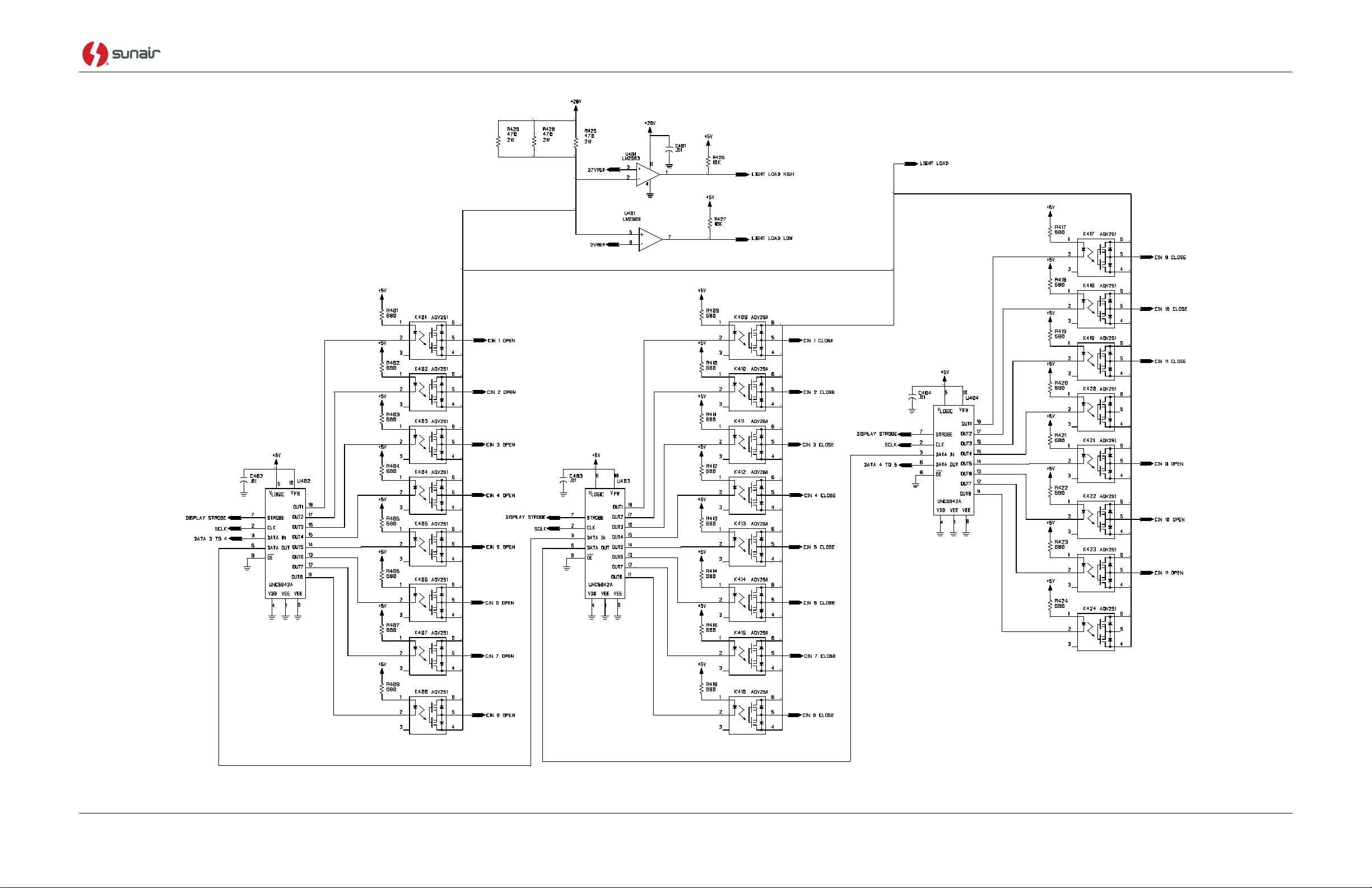
CU-9150
Figure 6.1-1. PC Assembly, Test Fixture, CU-9150 CPU
(Page 7 of 9)
Use or disclosure of information from this document is subject to the restrictions 6-15
indicated on the proprietary/confidentiality page of this document.
Page 100
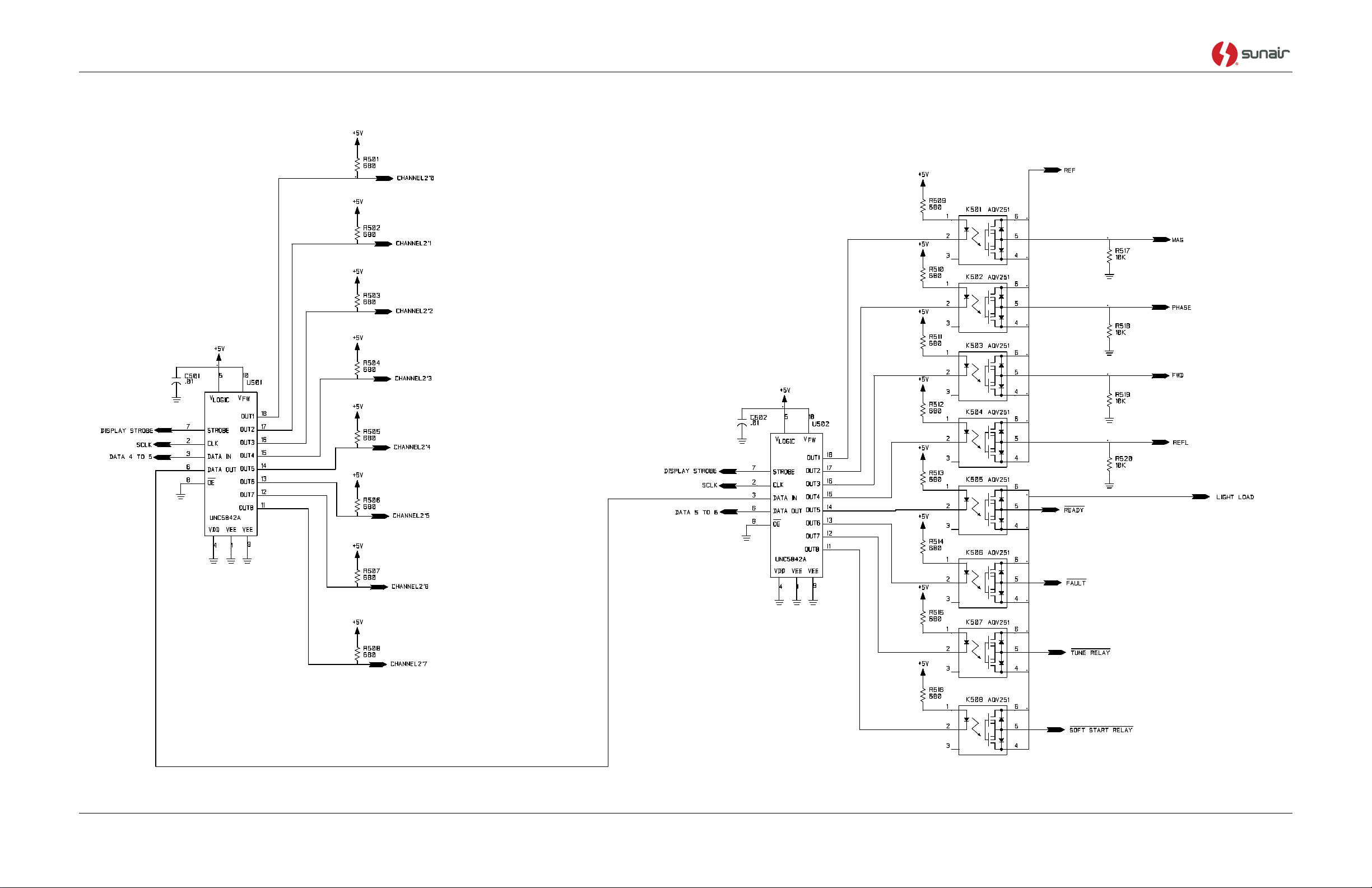
CU-9150
Figure 6.1-1. PC Assembly, Test Fixture, CU-9150 CPU
(Page 8 of 9)
6-16 Use or disclosure of information from this document is subject to the restrictions
indicated on the proprietary/confidentiality page of this document.
 Loading...