SUMMIT
MICROELECTRONICS, Inc.
Philips TriMedia™ Processor Companion Supervisor
With a 16K-bit 2-wire Serial Memory
SMS8198
FEATURES
• Designed to operate with the Philips
TriMedia Processor
• Coordinating the System Reset Function and
Providing the Processor’s Configuration
Memory
• Multiple V
Thresholds
TRIP
- No External Components Required
• Guaranteed Reset Assertion to V
CC
-1V
• Reset is an I/O
- Allows System Reset Clean up
- Provides a De-bounced Manual Reset Func-
tion
• Industry Standard 2-wire Serial Interface
• Hardware Write Lockout Function
• High Reliability
- Endurance: 100,000 write cycles
- Data Retention: 100 Years
OVERVIEW
The SMS8198 is a precision supervisory circuit designed
specifically as a companion chip for the Philips TriMedia
Processor family. The SMS8198 monitors the power
supply and holds the system in reset whenever VCC is
below the V
threshold.
TRIP
In addition to the supervisory function, the SMS8198 has
16K-bits of nonvolatile memory that is used by the
TriMedia processor as the boot memory.
The SMS8198 provides 16K-bits of memory that is accessible through the industry standard 2-wire serial interface.
By integrating a precision supervisory circuit and the
hardware WP input, the SMS8198 becomes the perfect
companion chip for the Philips TriMedia processor family.
Its functions are integral to the boot hardware operation of
the TriMedia processors.
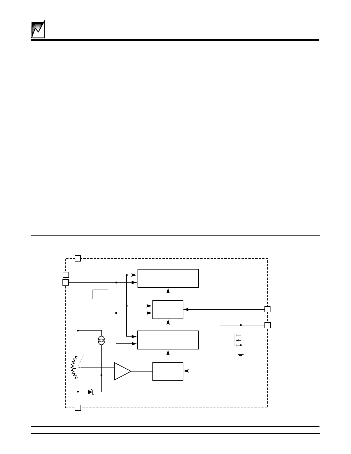
BLOCK DIAGRAM
V
CC
8
SCL
6
SDA
5
4
GND
1.26V
NONVOLATILE
MEMORY
ARRAY
WRITE
CONTROL
PROGRAMMABLE
RESET PULSE
GENERATOR
+
–
V
TRIP
RESET
CONTROL
2036 T BD 2.0
WP
7
TRI_RESET#
2
SUMMIT MICROELECTRONICS, Inc. • 300 Orchard City Drive, Suite 131 • Campbell, CA 95008 • Telephone 408-378-6461 • Fax 408-378-6586 • www.summitmicro.com
© SUMMIT MICROELECTRONICS, Inc. 2000
2036 5.0 4/18/00
1
Characteristics subject to change without notice

10K
WP
4.7K
4.7K
4.7K
AudioCamera
Tri
Media
Processor
SMS8198
VCR/Monitor
TRI_RESET#
SCL
SDA
SMS8198
PCI_RESET#
TRI_RESET#
System Boot
Local Reset
PCI Bus
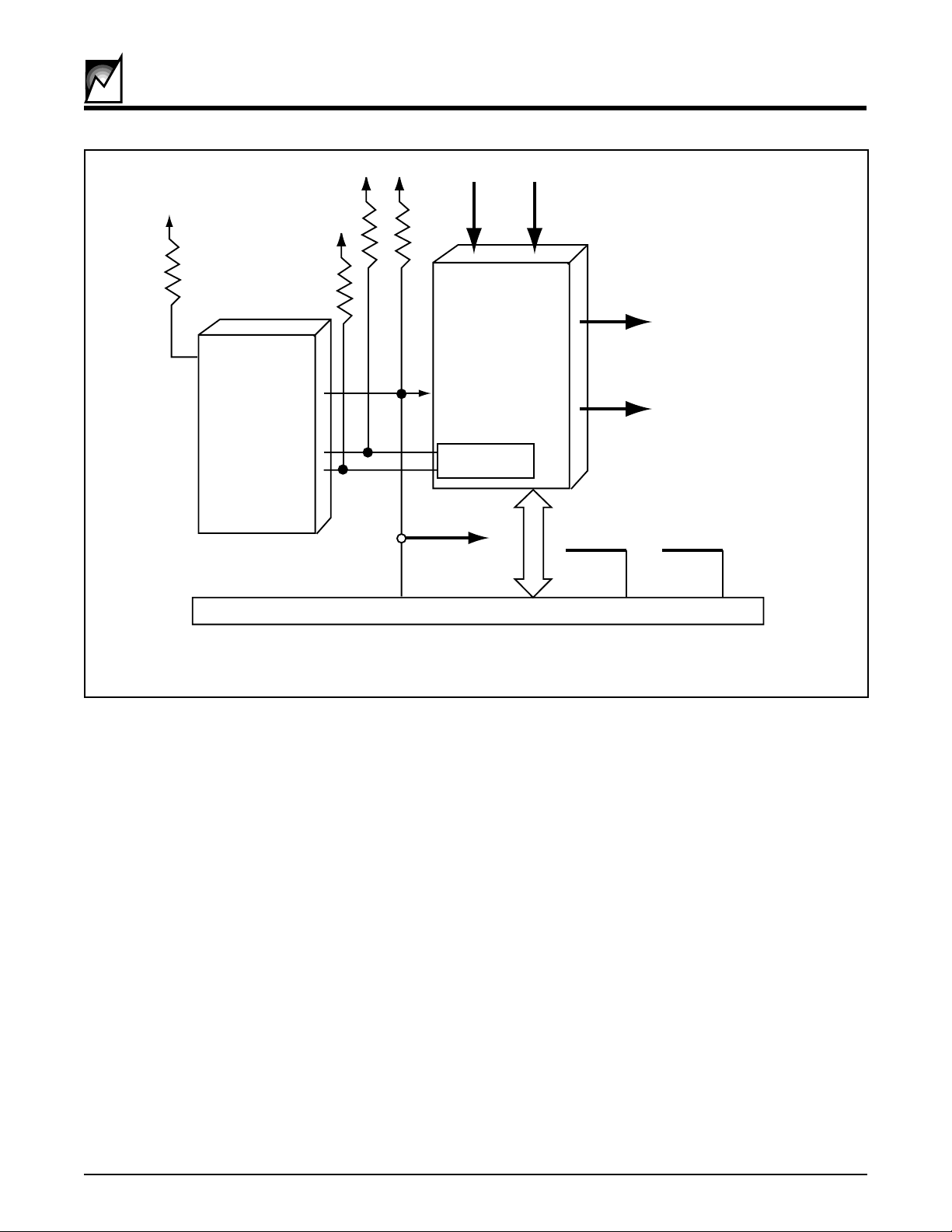
Figure 1. Typical Implementation of the SMS8198 and TriMedia Processor
The boot hardware operation begins with the assertion of
the reset signal TRI_RESET#. The TRI_RESET# output
from the SMS8198 is guaranteed to be valid at VCC -1.0V.
The reset output is asserted whenever VCC is less than the
V
threshold and will remain asserted after VCC is
TRIP
>V
for the duration of t
TRIP
. Whenever the
PURST
TRI_RESET# is active the memory will be write protected.
In addition to the reset write protection feature, pin 7 can
be tied to a pull-up to disable the write function of the
memory. This effectively turns the memory array into an
inexpensive boot ROM.
Audio
Block
Peripheral Peripheral
2036 ILL16.0
After reset is de-asserted, only the system boot block is
allowed to operate. At this point the TriMedia processor
takes over and begins to download data from the memory
array into its system boot block. The data downloaded
contains configuration data to set up the TriMedia processor and to load special ID information into the PCI configu-
ration space register. The ID information is published in
the PCI configuration register to provide the 16 bit Subsystem ID and Subsystem Vendor ID.
It should be noted that both the threshold and the t
pulse width are programmable. Not only does this provide
maximum flexibility to the designer, but, as the processor
operating voltage levels migrate downwards, the
SMS8198 can be programmed to following this downward
trend. The values can be selected from the ordering
information table and the devices specified as standard
off-the-shelf items.
PURST
2036 5.0 4/18/00
2

V
CC
TRI_RESET#
V
RVALID
V
TRIP
t
GLITCH
t
PURST
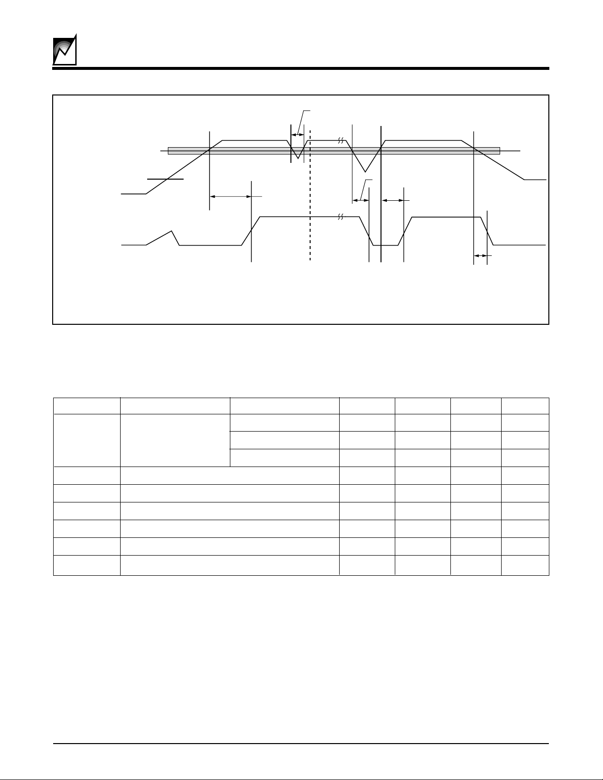
Figure 2. Reset Output Timing
t
RPD
t
PURST
SMS8198
t
RPD
2036 T fig02 2.0
RESET CIRCUIT AC and DC ELECTRICAL CHARACTERISTICS
TA = -40°C to +85°C
Symbol Parameter Part no. Suffix Min. Typ. Max. Unit
V
TRIP
Reset Trip Point A (or) Blank 4.250 4.375 4.5 V
B 4.50 4.625 4.75 V
2.7 2.55 2.65 2.75 V
t
PURST
t
RPD
V
RVALID
t
GLITCH
V
OLRS
V
OHRS
Reset Timeout 200 ms
V
to RESET Output Delay 5 µs
TRIP
RESET Output Valid to VCC min. Guarantee 1 V
Glitch Reject Pulse Width note 1 30 ns
RESET Output Low Voltage IOL = 1mA 0.4 V
RESET High Voltage Output IOH = 800µA
3
2036 5.0 4/18/00

SMS8198
PIN CONFIGURATIONS
NC
TRI_RESET#
NC
GND
PIN NAMES
SDA Serial Data I/O
SCL Serial Clock Input
TRI_RESET# Reset Output
GND Ground
V
CC
WP Write Protect
NC No Connect
8-Pin SOIC
1
2
3
4
8
7
6
5
2036 T PCon 2.0
Supply Voltage
V
CC
WP
SCL
SDA
TRI_RESET# - is an active low open drain output. It is
driven low whenever VCC is below V
. TRI_RESET# is
TRIP
also an input and can be used to debounce a switch input
or perform signal conditioning. The TRI_RESET# pin
does have an internal pull-up and should be left unconnected if the signal is not used in the system. However,
when the pin is tied to a system TRI_RESET# line an
external pull-up resistor should be employed.
Write Protect (WP) - All write operations can be disabled
by maintaining WP > VIH.
No Connects (NC) - The no connect inputs are unused by
the SMS8198; however, to insure proper operation they
can be unconnected or tied to ground. They must not be
tied to VCC.
ENDURANCE AND DATA RETENTION
The SMS8198 is designed for applications requiring up to
100,000 erase/write cycles and unlimited read cycles. It
provides 100 years of secure data retention, with or
without power applied, after the execution of 100,000
erase/write cycles.
RESET CONTROLLER DESCRIPTION
The device provides a precise reset output to a
microcontroller and it’s associated circuitry ensuring correct system operation during power-up/down conditions
and brownout situations. The output is open drain, allowing control of the reset function by multiple devices.
PIN DESCRIPTIONS
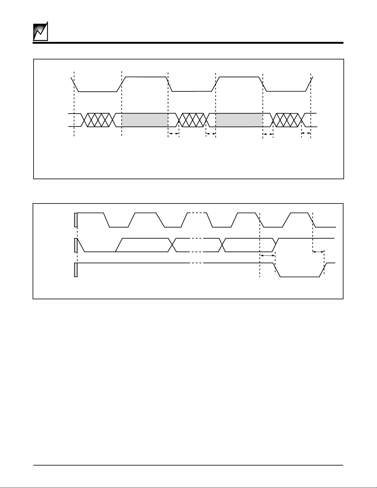
Serial Clock (SCL) - The SCL input is used to clock data
into and out of the device. In the WRITE mode, data must
remain stable while SCL is HIGH. In the READ mode, data
is clocked out on the falling edge of SCL.
Serial Data (SDA) - The SDA pin is a bidirectional pin
used to transfer data into and out of the device. Data may
change only when SCL is LOW, except START and STOP
conditions. It is an open-drain output and may be wireORed with any number of open-drain or open-collector
outputs.
During power-up the reset output remains in a fixed active
state until VCC passes through the reset threshold and
remains above the threshold for t
is valid whenever VCC is equal to or greater than 1V. If V
falls below the threshold for more than t
. The reset output
PURST
GLITCH
CC
the device
will immediately generate a reset and drive the output.
The reset pin is an I/O; therefore, forcing the pin to the
active state can also manually reset the device. Because
the I/O needs to be an open drain, the internal timer can
only be triggered by the leading edge of the input. The
resulting reset output will either be t
, or the externally
PURST
applied reset signal, whichever is longer. This can provide
an affective debounce or reset signal extender solution.
2036 5.0 4/18/00
4

SMS8198
SCL
SDA In
SCL from
Master
Data Output
from
Transmitter
Data Output
from
Receiver
Start
Condition
Data must
remain stable
while clock
is HIGH.
Figure 3. Input Data Protocol
1
t
HD:DAT
Change
of data
allowed
t
SU:DAT
Data must
remain stable
while clock
is HIGH.
8
t
HD:DAT
t
AA
2036 ILL4.0
9
ACKnowledge
t
AA
Figure 4. Acknowledge Response From Receiver
2036 ILL6.0
5
2036 5.0 4/18/00
 Loading...