SUMMIT SMS44G, SMS44S Datasheet
SUMMIT
MICROELECTRONICS, Inc.
SMS44
Highly Programmable V olta ge Supply Controller
and Supervisory Circuit
FEATURES INTRODUCTION
l Operational from any of four Voltage Monitoring
Inputs
l Programmable Closed Loop Power-up Cascad-
ing
l Programmability allows monitoring any voltage
between 0.9V and 6.0V with no external
components
l Programmable Watchdog Timer
l Programmable Longdog™ Timer
l Programmable Reset Pulse Width
l Programmable Nonvolatile Combinatorial Logic
for generation of Reset and Interrupt outputs
l Fault Status Register
l 4k-Bit Nonvolatile Memory
The SMS44 is a highly programmable voltage supply
controller and supervisory circuit designed specifically
for advanced systems that need to monitor multiple
voltages. The SMS44 can monitor four separate voltages
without the need of any external voltage divider circuitry.
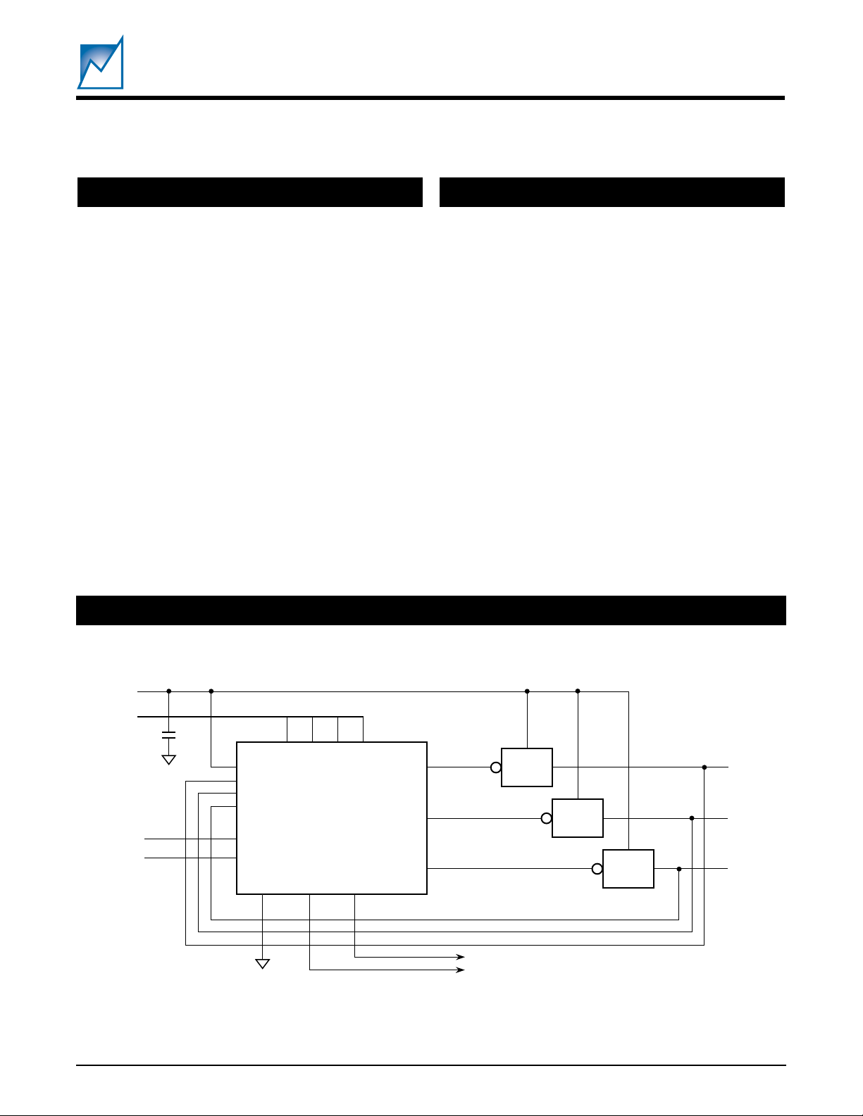
The SMS44 can also be used to enable DC/DC converters
or LDOs to provide a closed loop cascading of the
supplies during power -up.
The SMS44 watchdog timer has a user programmable
time-out period and it can be placed in an idle mode for
system initialization or system debug. All of the functions
are user accessible through an industry standard 2-wire
serial interface.
Programming of configuration, control and calibration
values by the user can be simplified with the interface
adapter and Windows GUI software obtainable from Summit Microelectronics.
Preliminary
SIMPLIFIED APPLICATION DRAWING
5V
2
I
C
0.01µF
Reset#
16
14
15
7
A2
V
0
2
V
1
3
V
2
V
3
1
MR#
WLDI
GND
RESET#
8
9
6
SDA
A1
SMS44
IRQ#
11
10
SCL
PUP#1
PUP#2
PUP#3
12
4
5
13
LDO
LDO
LDO
3.3V
2.5V
1.8V
2047 SAD 2.0
Closed Loop Power-up Supply Cascading
©SUMMIT MICROELECTRONICS, Inc., 2001 • 300 Orchard City Dr., Suite 131 • Campbell, CA 95008 • Phone 408-378-6461 • FAX 408-378-6586 • www.summitmicro.com
Characteristics subject to change without notice 2047 4.0 6/7/01
1
FUNCTIONAL BLOCK DIAGRAM
MR#
1
70kΩ
V
16
0
NV DAC
+
–
REF
V
2
1
NV DAC
+
–
REF
V
3
2
NV DAC
+
–
REF
V
14
3
NV DAC
+
–
REF
RESET
IRQ
RESET
IRQ
RESET
IRQ
RESET
IRQ
CONFIGURATION
REGISTER
CONFIGURATION
REGISTER
PROGRAMMABLE
RESET PULSE
GENERATOR
PROGRAMMABLE
LONGDOG
TIMER
PROGRAMMABLE
WATCHDOG
TIMER
V
CC
70kΩ
PROGRAMMABLE
POWER
CASCADING
SERIAL
BUS
CONTROL
LOGIC
4K-BIT NV
MEMORY
SMS44
Preliminary
V
CC
70kΩ
11
70kΩ
70kΩ
4
5
13
9
10
7
6
70kΩ70kΩ
V
CC
70kΩ
12
15
70kΩ
RESET#
PUP#1
PUP#2
PUP#3
SDA
SCL
A2
A1
IRQ#
WLDI
8
GND
CASCADING
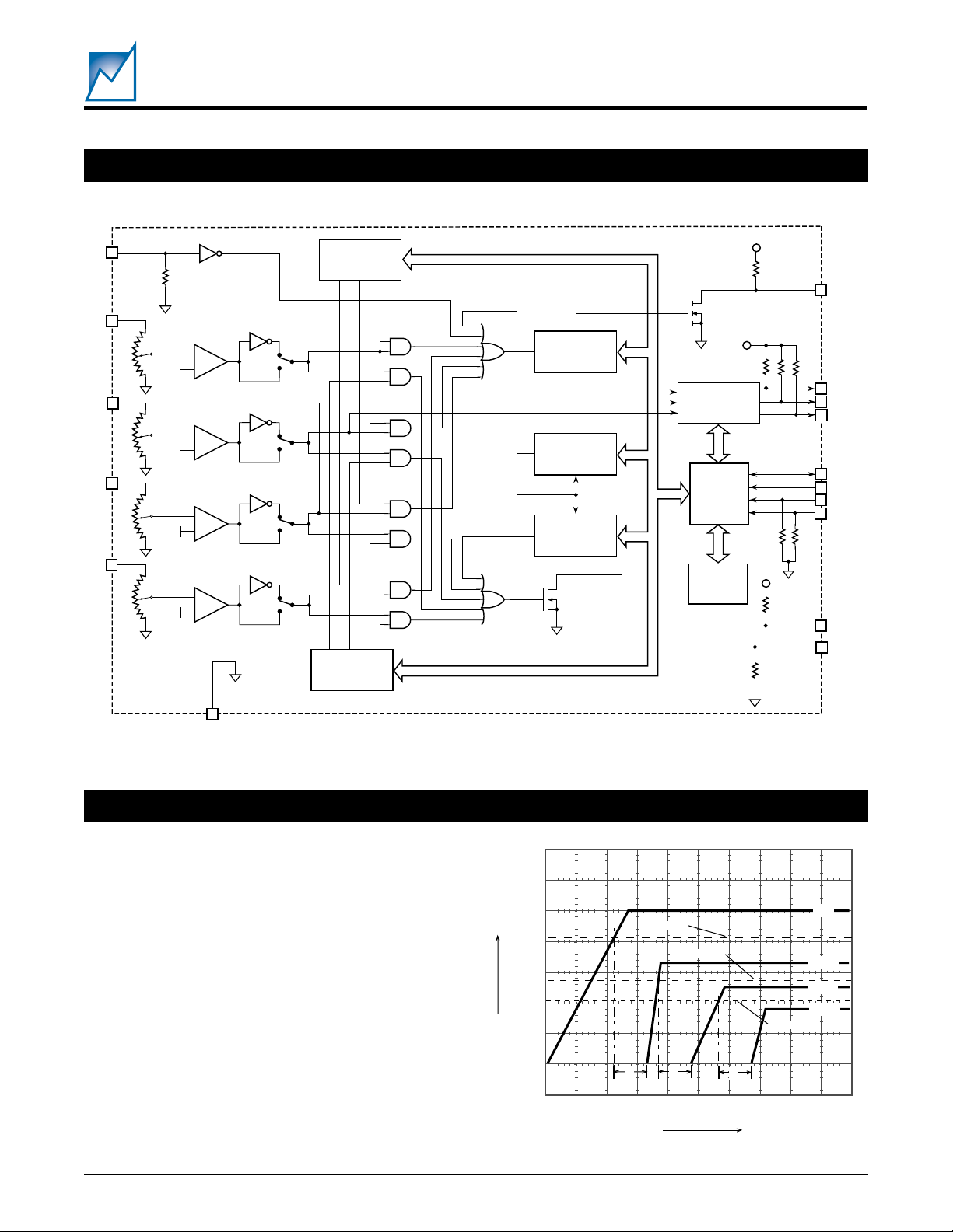
If a specific order in which the supplies are turned on and
brought up to their valid voltage levels is needed, time
based sequencing will not suffice. In this case supply
cascading should be utilized, where the supplies are
enabled a certain period of time after the previous voltage
has reached its minimum valid level. Figure 1 shows that
each succeeding voltage must reach its minimum valid
level before the timer is started to time the interval, t, for
the next voltage. The duration of each t is programmable.
The next supply is not enabled until the timer has elapsed.
See also Figure 5.
2047 BD 4.0
6V
5V
5V Valid
4V
V
2V
0V
t
3.3V Valid
t
3.3V
2.5V
1.8V
2.5V Valid
t
T
2047 Fig01
Figure 1. Cascading Power Supplies
2
2047 4.0 6/7/01
SUMMIT MICROELECTRONICS, Inc.
PIN CONFIGURATION PIN NAMES
SMS44
Preliminary
MR#
V
V
PUP#1
PUP#2
A1
A2
GND
16-Pin SOIC or
16-Pin SSOP
1
2
1
3
2
4
5
6
7
8
16
15
14
13
12
11
10
9
2047 PCon 2.0
V
0
WLDI
V
3
PUP#3
IRQ#
RESET#
SCL
SDA
niPemaNnoitcnuF
1#RMtupniteserlaunaM
2V
3V
1
2
41#PUPtuptuodettimreppurewoP
52#PUPtuptuodettimreppurewoP
61AtupnisserddA
72AtupnisserddA
8DNGnruterylppusrewoP
9ADSO/IatadlaireS
01LCSkcolcatadlaireS
11#TESERtuoteseR
21#QRItuotpurretnI
313#PUPtuptuodettimreppurewoP
41V
51IDLW
61V
3
tpurretni
0
tupnirotinomdnaylppusegatloV
tupnirotinomdnaylppusegatloV
tupnirotinomdnaylppusegatloV
remitgodgnol/godhctaW
tupnirotinomdnaylppusegatloV
2047 Pins Table 2.0
RECOMMENDED OPERATING CONDITIONS
Temperature –40ºC to 85ºC.
Voltage 2.7V to 5.5V
SUMMIT MICROELECTRONICS, Inc.
2047 4.0 6/7/01
3
ABSOLUTE MAXIMUM RATINGS*
SMS44
Preliminary
Temperature Under Bias ......................–55°C to 125°C
Storage Temperature ...........................–65°C to 150°C
Lead Solder Temperature (10s) .........................300 °C
Terminal Voltage with Respect to GND:
V0, V1, V2, and V3.......... –0.3V to 6.0V
All Others ...................... –0.3V to 6.0V
*COMMENT
Stresses beyond the listed Absolute Maximum Ratings may cause
permanent damage to the device. These are stress ratings only, and
functional operation of the device at these or any other conditions
outside those listed in the operational sections of this specification is not
implied. Exposure to any absolute maximum rating for extended
periods may affect device performance and reliability.
DC OPERATING CHARACTERISTICS
(Over Recommended Operating Conditions; Voltages are relative to GND)
lobmySretemaraPsetoN.niM.pyT.xaMtinU
-tuoteserdilavaotsrefer.nimV1
detareneggniebtup
V
CC
I
CC
V
HTP
egnaR
V
HTP
V
TSYH
V
LO
egnar
V
TSR
tnerrucylppuS
siseretsyh 03Vm
egatlovylppusgnitarepO
ta:snoitarepoetirw/daeryromeM
taebtsumstupniVehtfoenotsael
Vevobaro
≤ V;V5.5
V
CC
V
3
.nim
CC
V;V7.4tnioppirt
0
V=#RM;DNG=
CC
1V,2
stuptuolla;
,
gnitaolf
yromemroretsigernoitarugifnoC
ssecca
dlohserhtelbammargorP
V
3
)stnemercniVm02(
VegnaregatlovdlohserhtteseR
ot
0
dlohserhtelbammargorP5.2– V
V,Am2.1=
I
tuptuoegatlovwoL
KNIS
I
KNIS
≥ V7.23.0V
CC
V,Aµ002=
CC
V2.1=3.0V
1OTR0OTR
0.15.5V
7.25.5V
002004Aµ
3Am
9.00.6V
HTP
5.2%
00025203sm
t
OTRP
htdiw
eslupteserelbammargorP
01530556sm
1056001531sm
11031002072sm
t
TSRD
4
yaled#TESERotniVevirdrevoVm00102sµ
2047 Elect TableA 4.2
2047 4.0 6/7/01
SUMMIT MICROELECTRONICS, Inc.
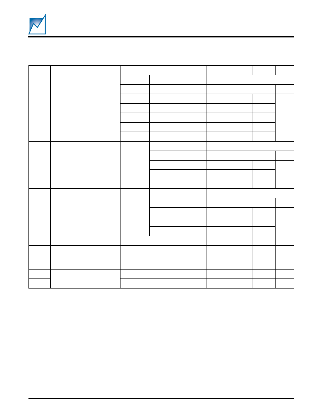
lobmySretemaraPsetoN.niM.pyT.xaMtinU
2DW1DW0DW
000 FFO —
011 004
t
OTDWP
doirepremit
godhctaWelbammargorP
100 008
101 0061
110 0023
111 0046
1DL0DL
00 FFO —
t
OTDLP
doirepremit
godgnoLelbammargorP
01 0061
11 0046
SMS44
Preliminary
sm
sm10 0023
1-X#PUP0-X#PUP
00 FFO —
t
X
YLDP
V
HTP
tuo#PUPot
morfyaledelbammargorP
01 52
sm10 05
11 001
I
RM
T
RM
T
TSRRMD
V
LI
V
HI
wol#TESER
tnerrucpullup#RM 001Aµ
htdiwesluptupni#RM 003sn
otwol#RMmorfyaleD
002sn
dlohserhttupnI
7.0 × V
CC
6.0V
V
2047 Elect TableB 4.2
SUMMIT MICROELECTRONICS, Inc.
2047 4.0 6/7/01
5
PIN DESCRIPTIONS
SMS44
Preliminary
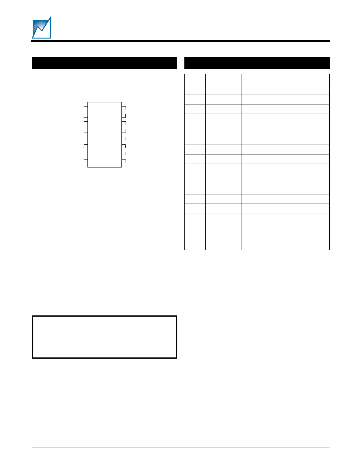
V0, V1, V2, V3 (16, 2, 3, 14)
These inputs are used as the voltage monitor inputs and
as the voltage supply for the SMS44. Internally they are
diode ORed and the input with the highest voltage
potential will be the default supply voltage.
The RESET# output will be true if any one of the four inputs
is above 1V. However, for full device operation at least
one of the inputs must be at 2.7V or higher.
The sensing threshold for each input is independently
programmable in 20mV increments from 0.9V to 6.0V.
Also, the occurrence of an under- or over-voltage condition that is detected as a result of the threshold setting can
be used to generate subsequent action(s), such as
RESET# or IRQ#. The programmable nature of the
threshold voltage eliminates the need for external voltage
divider networks.
GND
Power supply return.
MR# (1)
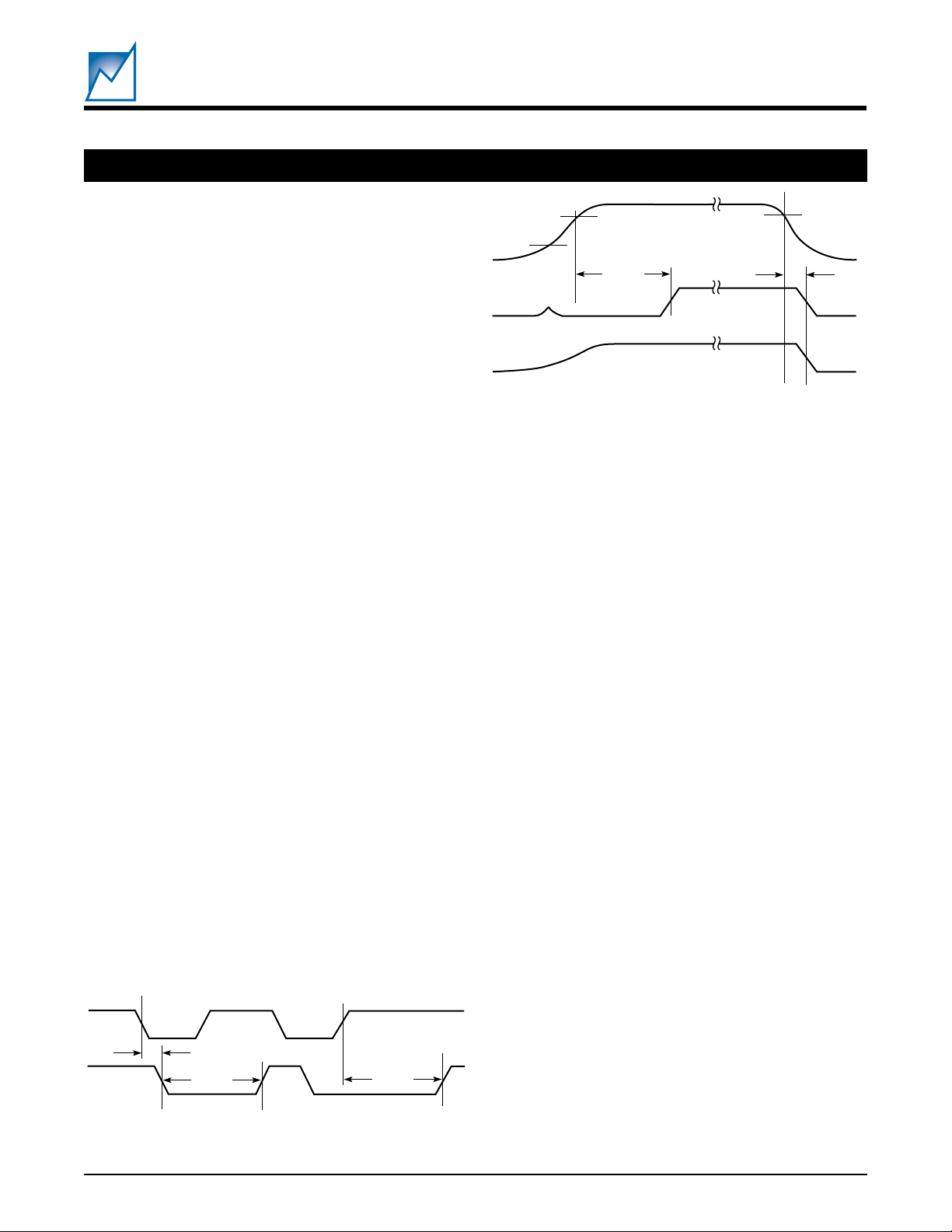
The manual reset input always generates a RESET#
output whenever it is driven low. The duration of the
RESET# output pulse will be initiated when MR# goes low
and it will stay low for the duration of MR# low plus the
programmed reset time-out period (t
). If MR# is
PRTO
brought low during a power-on cascade of the PUP#s the
cascade will be halted for the reset duration, and will then
resume from the point at which it was interrupted. MR#
must be held low during a configuration register Write or
Read. This signal is pulled down internally through a 70kΩ
resistor, consequently the part is normally in reset mode
when powered down.
RESET# (11)
The reset output is an active low open drain output. It will
be driven low whenever the MR# input is low or whenever
an enabled under-voltage or over-voltage condition ex-
MR#
t
DMRRST
RESET#
t
PRTO
t
PRTO
V
RST
2047 Fig03 2.0
V0 — V
RESET#
IRQ#
V
3
PTH
t
PRTO
t
D
Figure 3. RESET# Timing with IRQ#
ists, or when a longdog timer expiration exists. The four
voltage monitor inputs are always functioning, but their
ability to generate a reset is programmable (configura-
tion register 4). Refer to Figures 2 and 3 for a detailed
illustration of the relationship between MR#, IRQ#, RESET# and the VIN levels. This signal is pulled up internally
through a 70kΩ resistor.
IRQ# (12)
The interrupt output is an active low open-drain output. It
will be driven low whenever the watchdog timer times out
or whenever an enabled under-voltage or over-voltage
condition on a V input exists (configuration register 6).
This signal is pulled up internally through a 70kΩ resistor.
WLDI (15)
Watchdog and longdog timer interrupt input. A low to high
transition on the WLDI input will clear both the watchdog
and longdog timers, effectively starting a new time-out
period. This signal is pulled down internally through a
70kΩ resistor.
If WLDI is stuck low and no low-to-high transition is
received within the programmed t
PWDTO
period (programmed watch dog time-out) IRQ# will be driven low. If
a transition is still not received within the programmed
t
period (programmed longdog time-out) RESET#
PLDTO
will be driven low. Refer to Figure 4 for a detailed
illustration.
Holding WLDI high will block interrupts from occurring but
will not block the longdog from timing out and generating
a reset. Refer to Figure 4 for a detailed illustration of the
relationship between IRQ#, RESET#, and WLDI.
2047 Fig02 2.0
Figure 2. RESET# Timing with MR#
6
2047 4.0 6/7/01
SUMMIT MICROELECTRONICS, Inc.
 Loading...