Summit SMS1242 Technical data

© SUMMIT MICROELECTRONICS, Inc. 2000 • 300 Orchard City Drive, Suite 131 • Campbell, CA 95008 • Phone 408-378-6461 • Fax 408-378-6586 • www.summitmicro.com
1
Characteristics subject to change without notice
2038 2.0 6/8/00
SUMMIT
MICROELECTRONICS, Inc.
SMS1242
FEATURES
• Supply voltage monitor
- Nominal V
RST
of 2.45V, 2.65V, 2.95V, 4.45V,
4.55V or 4.65V
- RESET# Outputs Guaranteed true at VCC = 1V
- 150ms Reset Delay Time
• Second voltage monitor
-V
SENSE
Input
- 1.25V threshold ±1%
• Manual Reset Input
• Includes 16k-bits nonvolatile memory
- Industry standard 2-wire serial interface
2.5V, 3V, 3.3V & 5V Dual Voltage, Dual Reset
Microprocessor Supervisory Circuits
OVERVIEW
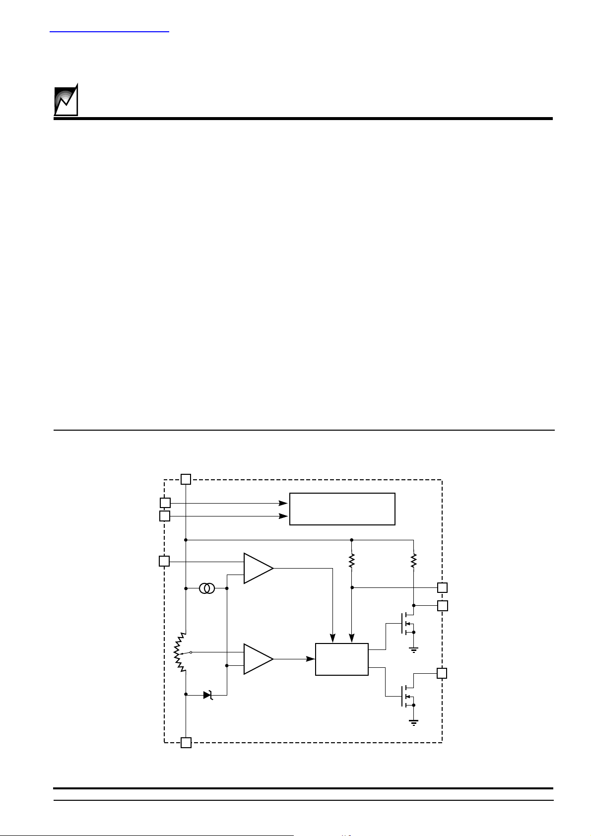
The SMS1242 microprocessor supervisory circuit reduces the complexity and number of components required
to monitor the supply voltage in +5V, +3V and +2.5V
systems. The SMS1242 will significantly improve system
reliability and accuracy when compared to implementing
the same functions with discrete components.
The SMS1242 provides reset output during power-up,
power-down, and brown-out conditions. It has a 1.25V
threshold input detector for power-fail warning, low battery
detection, or monitoring a secondary power supply. The
part also integrates a separate active low manual reset
input.
It also has 16k-bits of nonvolatile memory accessible over
an industry standard 2-wire serial interface.
FUNCTIONAL BLOCK DIAGRAM
+
–
GND
V
CC
8
4
RESET1#
2
V
TRIP
RESET
GENERATOR
7
1.25V
SCL
6
SDA
5
2038 BD 2.0
NONVOLATILE
MEMORY
ARRAY
V
SENSE
3
MR#
1
+
–
RESET2#
查询SMS1242S-F供应商

2
SMS1242
2038 2.0 6/8/00SUMMIT MICROELECTRONICS, Inc.
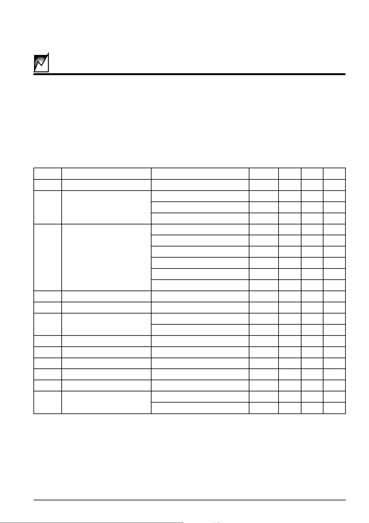
ABSOLUTE MAXIMUM RATINGS*
Temperature Under Bias –55°C to 125°C
Storage Temperature –65°C to 150°C
Terminal Voltage (With Respect to Ground)–0.3V to 6V
Lead Solder Temperature (10 secs) 300°C
*COMMENT
Stresses above those listed under Absolute Maximum Ratings
may cause permanent damage to the device. These are stress
ratings only, and functional operation of the device at these or
any other conditions outside those listed in the operation sections of this specification is not implied. Exposure to any absolute maximum rating for extended periods may affect device
performance and reliability.
2038 Elect Table 2.0
lobmySretemaraPsnoitidnoC.niM.pyT.xaMstinU
V
CC
egatlovylppusgnitarepO15.5V
I
CC
tnerrucylppuS
<V6.3V
CC
5.5<V 5205Aµ
>V6.3V
CC
5205Aµ
)ylno3421SMS(sseccayromeM3Am
V
TSR
dlohserhtteseR
AnoitpoeciveD573.4524.4574.4V
BnoitpoeciveD526.4576.4527.4V
CnoitpoeciveD524.4574.4525.4V
DnoitpoeciveD524.2054.2574.2V
EnoitpoeciveD526.2056.2576.2V
FnoitpoeciveD529.2059.2579.2V
V
TSYH
V
TSR
sisiretsyH 05Vm
t
TSR
htdiweslupteseR001051002sm
V
LO
egatlovwoltuptuo#1TESER
I
KNIS
V,Am2.1=
CC
V=
TSR
.nim3.0V
I
KNIS
V,Aµ002=
CC
V2.1=3.0V
I
RM
tnerrucpullup#RM 001Aµ
t
RM
htdiweslup#RM05sn
V
LI
dlohserhttupni#RM 6.0V
V
HI
dlohserhttupni#RM7.0 × V
CC
V
V
SNS
V
ESNES
dlohserhttupniV
CC
=V
TSR
V,.nim
ESNES
gnillaf02.152.103.1V
V
CC
egatlovwoltuptuo#2TESER
I
KNIS
V,Am2.1=
CC
V=
TSR
.nim3.0V
I
KNIS
V,Aµ002=
CC
V2.1=4.0V

3
2038 2.0 6/8/00
SMS1242
SUMMIT MICROELECTRONICS, Inc.
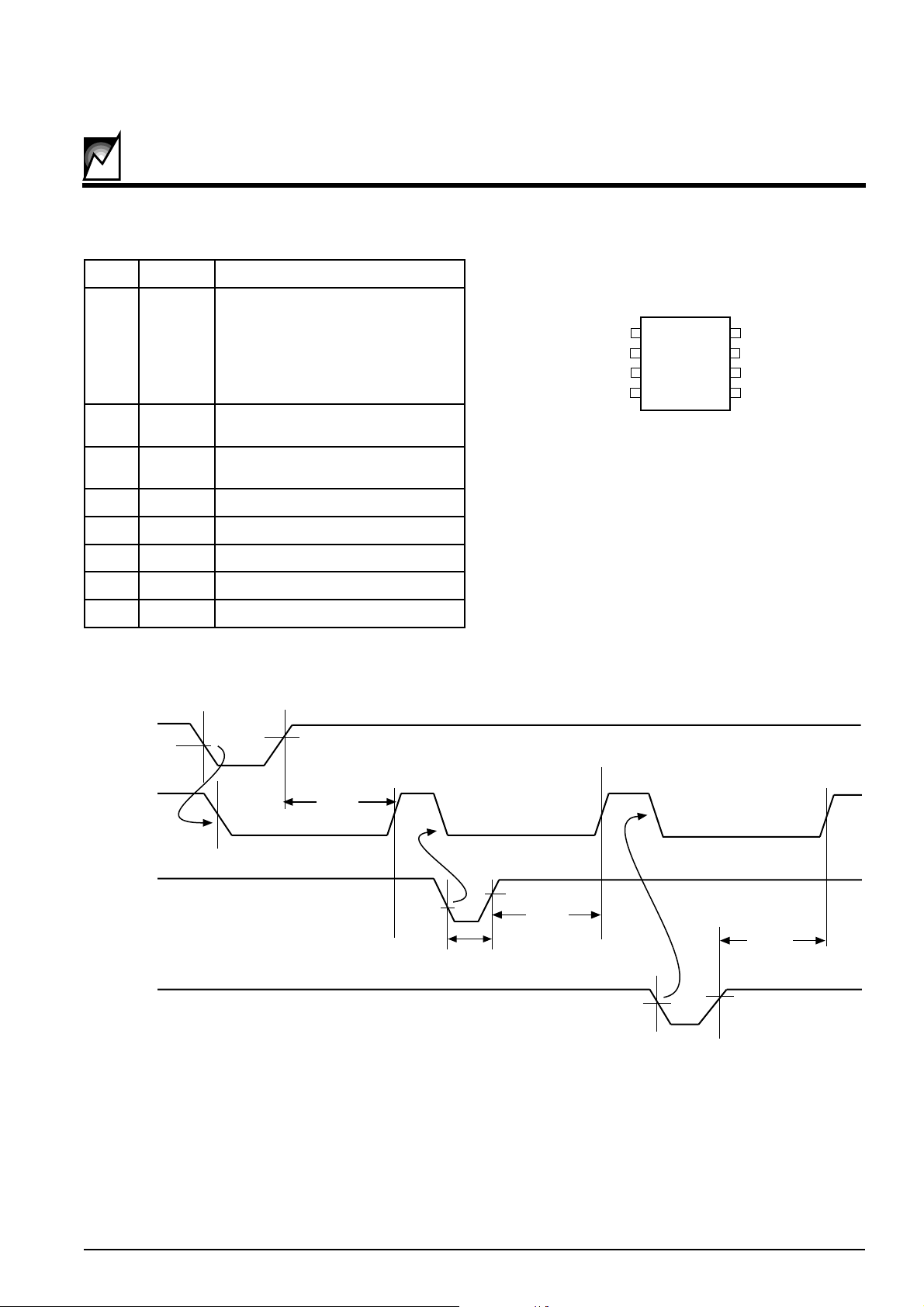
PIN CONFIGURATION
PIN NAMES
2038 Pin Table 2.0
RESET1#
RESET2#
V
SENSE
GND
V
CC
MR#
SCL
SDA
1
2
3
4
8
7
6
5
8-Pin SOIC
2038 T PCon 2.0
Figure 1. Reset Waveforms
niPlangiSnoitcnuF
1#1TESER
.pullupkaewhtiwtuptuowolevitcA
:ybwolnevirDV
ESNES
-hserhtwoleb
ro;dloV
CC
elihwdlohserhtwoleb
sniameR.dlohserhtwolebsi#RM
retfasm051rofwolV
ESNES
ro,V
CC
.dlohserhtevobasi,#RMdna
2#2TESER
nepotpecxe,#1teseRsaemaS
noitcennocniard
3V
ESNES
ehtroftupnirotceteddlohserhT
steseR
4DNGdnuorG
5DNG/ADSdnuorgro,O/IataD3421SMS
6DNG/LCSdnuorgro,kcolCataD3421SMS
7#RMsteseRroftupnilaunaM
8V
CC
egatlovylppuS
V
CC
RESET#
MR#
V
SENSE
V
RST
V
RST
t
RST
t
RST
t
RST
V
SNS
V
IL
V
IH
t
MR
2038 T Fig01 2.0

4
SMS1242
2038 2.0 6/8/00SUMMIT MICROELECTRONICS, Inc.
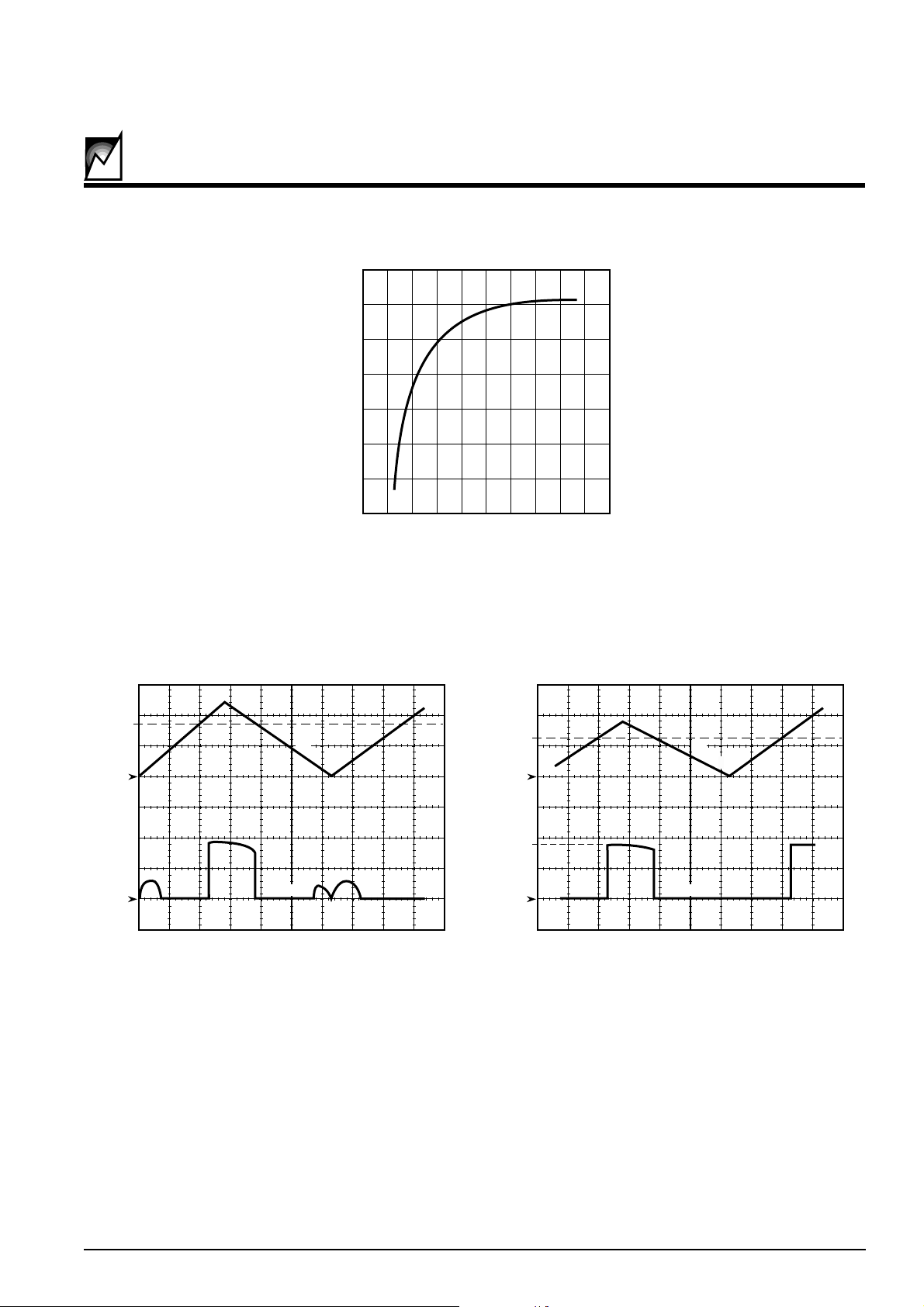
Figure 4. RESET Output vs. V
SENSE
Figure 3. RESET Output vs. Supply
Figure 2. Supply Voltage Noise Rejection, V
RST
=4.55V, TA = 25ºC
02
6
108
4
31
75
9
GLITCH AMPLITUDE (V)
PULSE WIDTH (ms)
4.5
4.4
4.3
4.2
4.1
4.0
3.9
3.8
2038 Fig02 2.0
V
RST
0V
0V
RESET#
V
CC
500ms/Div.
1.25V
0V
2V
0V
RESET#
V
SENSE
V
CC
 Loading...