SUMMIT SMP9317S Datasheet

SUMMIT
MICROELECTRONICS, Inc.
Nonvolatile DACPOT™ Electronic Potentiometer
With Up/Down Counter Interface
FEATURES
• Digitally Controlled Electronic Potentiometer
• 7-Bit Digital-to-Analog Converter (DAC)
– Independent Reference Inputs
– Differential Non-Linearity - +0.5LSB
– Integral Non-Linearity - +1LSB
•V
Value in EEPROM for Power-On Recall
OUT
– Equivalent to 128-Step Potentiometer
• Unity Gain Op Amp Drives ±100µA
• Simple Trimming Adjustment
– Up/Down Counter Style Operation
• Low Noise Operation
• “Clickless” Transitions between DAC Steps
• No Mechanical Wearout Problem
– 1,000,000 Stores (typical)
– 100 Year Data Retention
• Operation from +2.7V to +5.5V Supply
OVERVIEW
The SMP9317 DACPOT™ trimmer is a 7-bit nonvolatile
DAC designed to replace mechanical potentiometers.
The SMP9317 includes a unity-gain amplifier to buffer the
DAC output and enables V
The DACPOT trimmer operates over a supply voltage
range of 2.7V to 5.5V.
The SMP9317’s simple up/down counter input provides
an ideal interface for automatic test equipment to dither
and monitor the V
quick and consistent calibration of even the most sophisticated systems.
The SMP9317 is a pin-compatible performance upgrade
for other industry nonvolatile potentiometers. The
SMP9317 offers higher resolution than these devices and
provides ‘clickless’ transitions of V
SMP9317
to swing from rail to rail.
OUT
voltage. This interface allows for
OUT
.
OUT
• Ultra-Low Power, 0.5mW max at +5V
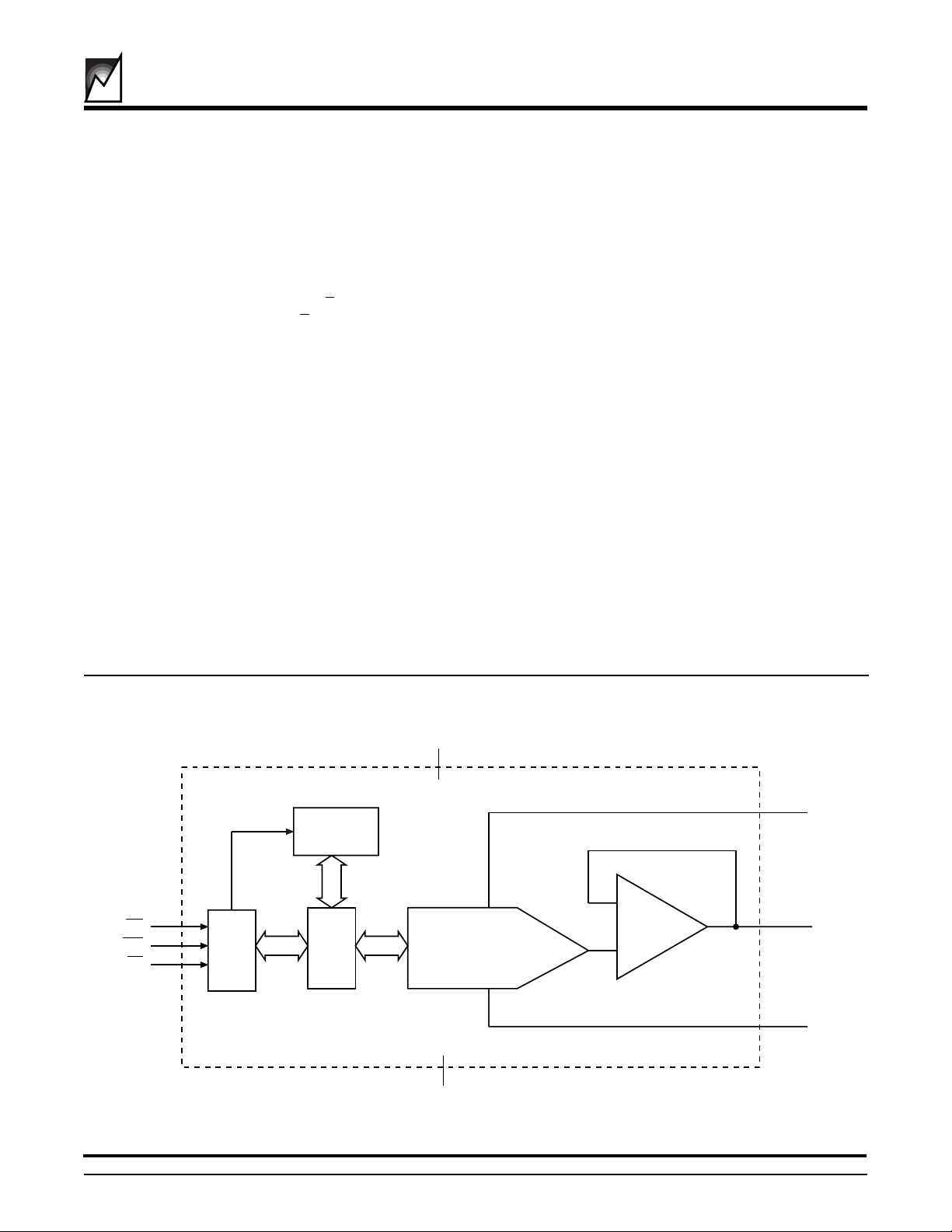
FUNCTIONAL BLOCK DIAGRAM
7-bit E2 PROM
UP/DN
INC
CS
Counter
&
Write
Control
7-bit
Data
Register
V
DD
7-bit DAC
-
+
AMP
V
V
H
OUT
V
L
GND
2031 ILL2.0
SUMMIT MICROELECTRONICS, Inc. • 300 Orchard City Drive, Suite 131 • Campbell, CA 95008 • Telephone 408-378-6461 • Fax 408-378-6586 • www.summitmicro.com
© SUMMIT MICROELECTRONICS, Inc. 1998
2031-04 12/4/98
1
Characteristics subject to change without notice

SMP9317
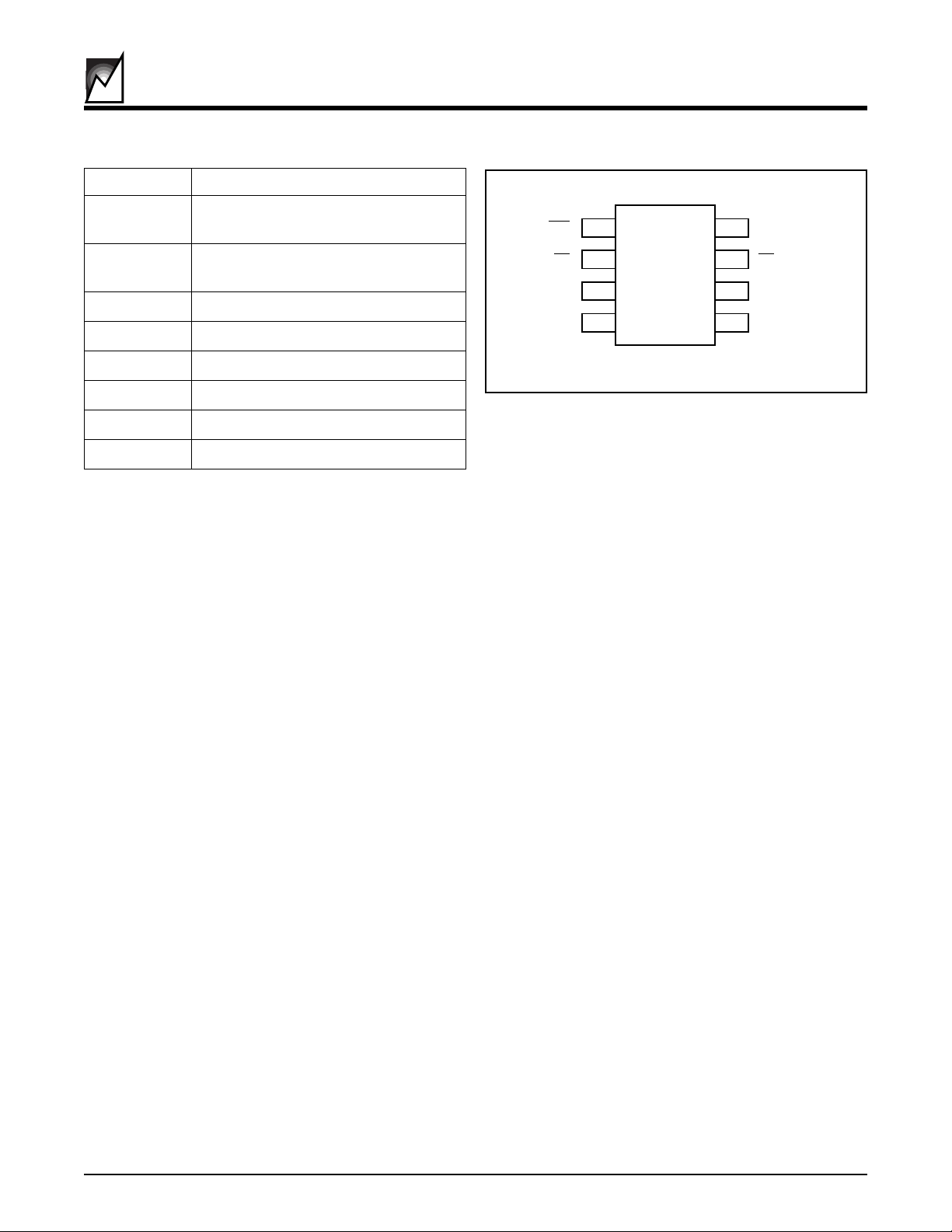
PIN NAMES
Symbol Description
INC Increment Input, High to Low
Edge Trigger
UP/DN Up/Down Input controlling relative
V
movement
OUT
V
H
V+ reference input
GND Analog and Digital Ground
V
OUT
V
L
Trimmed Voltage Output
V- reference input
CS Active low chip select input
V
DD
Supply Voltage (2.7V to 5.5V)
Analog Section
The SMP9317 is a 7-bit, voltage output digital-to-analog
converter (DAC). The DAC consists of a resistor network
that converts a 7-bit value into equivalent analog output
voltages in proportion to the applied reference voltage.
Reference Inputs
The voltage differential between the VL and VH inputs
sets the full-scale output voltage range. VL must be equal
to or greater than ground (i.e. a positive voltage). VH must
be greater than VL and less than or equal to VDD. See
table on page 3 for guaranteed operating limits.
Output Buffer Amplifier
The voltage output is from a precision unity-gain follower
that can slew up to 1V/µs.
Digital Interface
The interface is designed to emulate a simple up/down
counter, but instead of a parallel count output, a
ratiometric voltage output is provided.
Chip Select (
CSCS
CS) is an active low input. Whenever CS is
CSCS
high the SMP9317 is in standby mode and consumes the
least power. This mode is equivalent to a potentiometer
that is adjusted to the required setting. When CS is low
the SMP9317 will recognize transitions on the INC input
and will move the V
either toward the VH reference or
OUT
toward the VL reference depending upon the state of the
UP/DN input.
The host may exit an adjustment routine in two ways:
deselecting the SMP9317 while INC is low will not perform a store operation (a subsequent power cycle will
recall the original data); deselecting the SMP9317 while
INC is high will store the current V
setting into non-
OUT
volatile memory.
PINOUT
INC
UP/DN
V
GND
Increment (
1
2
3
H
4
INCINC
INC) is an edge triggered input. Whenever
INCINC
8
7
6
5
2031 ILL1.0
V
CS
V
V
DD
L
OUT
CS is low and a high to low transition occurs on the INC
input, the V
voltage will either move toward VH or V
OUT
depending upon the state of the UP/DN input.
UP/Down (UP/
DNDN
DN) is an input that will determine the V
DNDN
OUT
movement relative to VH and VL. When CS is low, UP/DN
is high and there is a high to low transition on INC, the
V
voltage will move (1/128th x VH-VL) toward VH.
OUT
When CS and UP/DN are low, and there is a high to low
transition on INC, the V
will move (1/128th x VH-VL)
OUT
toward VL.
Power–Up/Power–Down Conditions
On power–up the SMP9317 loads the value of EEPROM
memory into the wiper position register. The value in the
register is changed using the CS, INC, and UP/DN pins.
The new data in the register will be lost at power-down
unless CS was brought high, with INC high, to initiate a
store operation after the last increment or decrement. On
the next device power–up, the value of EEPROM memory
will be loaded into the wiper position register. During
power-up the SMP9317 is write-protected in two ways:
1) A power-on reset, that trips at approximately 2.5V,
holds CS and INC high internally.
2) Resistor pull-ups on all logic inputs prevent data
change if the inputs are floating.
Data Retention
The SMP9317 is guaranteed to perform at least
1,000,000 writes to EEPROM before a wear–out condition can occur. After EEPROM wearout, the SMP9317
continues to function as a volatile digital-potentiometer.
The wiper position can be changed during powered
conditions using the digital interface. However, on power–
up the wiper–position will be indeterminate.
On shipment from the factory, Summit Microelectronics
does not specify any EEPROM memory value. The value
must be set by the customer as needed.
L
2031-04 12/4/98
2
 Loading...