SUMMIT
MICROELECTRONICS, Inc.
SML2108
Dual Loop Laser Diode Adaptive Power Controller
with Look Up Table
FEATURES
!!
! Dual Closed-loop Control of Laser Diode Mean
!!
Power and Extinction Ratio
!!
! Automatic Power Control (APC) with Integrated
!!
10-Bit Programmable Offset
""
" Automatic Initial Bias Optimization
""
!!
! Integrated Bias Current Monitor
!!
""
" Monitors & Measures Laser Temperature
""
Directly
""
" Eliminates Need for External Thermistor &
""
Thermal Coupling Issues
""
" Alarm Output on Over-temperature Condition
""
!!
! Adaptive Modulation Control (AMC)
!!
""
" Adjusts Modulation Current as a Function of
""
the Laser Temperature
""
" 256 Independent Compensation Values
""
""
" Integrated 8-Bit Modulation Control DAC
""
!!
! Current Available: 0 to 100mA Sink or Source
!!
!!
! Electronic Calibration Through 2-wire Interface
!!
!!
! 3V or 5V Operation
!!
!!
! Typical Applications: 2.5GHz Transceivers;
!!
200 pin/300 pin 10GIG Sonet MSA Compliant;
10GbE XENPAK-compliant Transponders
DESCRIPTION
The SML2108 is an adaptive power controller for laser
diodes. It is the industry's first integrated device that can
directly monitor and measure a laser diode's temperature,
and provide a variable modulation current. The
SML2108's integrated active feedback loop is used to
calibrate and control the mean and modulation power of
high speed, high power laser diodes.
Inherent manufacturing tolerances introduce variations
of performance in laser diodes. These variations, combined with parametric changes over the laser’s extreme
temperature range and laser aging, call for an efficient
temperature compensation scheme. Using an internal
digital control loop and a programmable nonvolatile compensation lookup table, the SML2108 provides the most
optimum adaptive power control with a minimum number
of external components.
The SML2108 removes the need for any manual calibration of the laser control circuit, which is currently the
industry standard practice. All calibration values are
programmed through the 2-wire communication interface,
which can be controlled by most production ATE equipment.
Programming of configuration, control and calibration
values by the user can be simplified with the interface
adapter and Windows GUI software obtainable from Summit Microelectronics.
PRELIMINARY
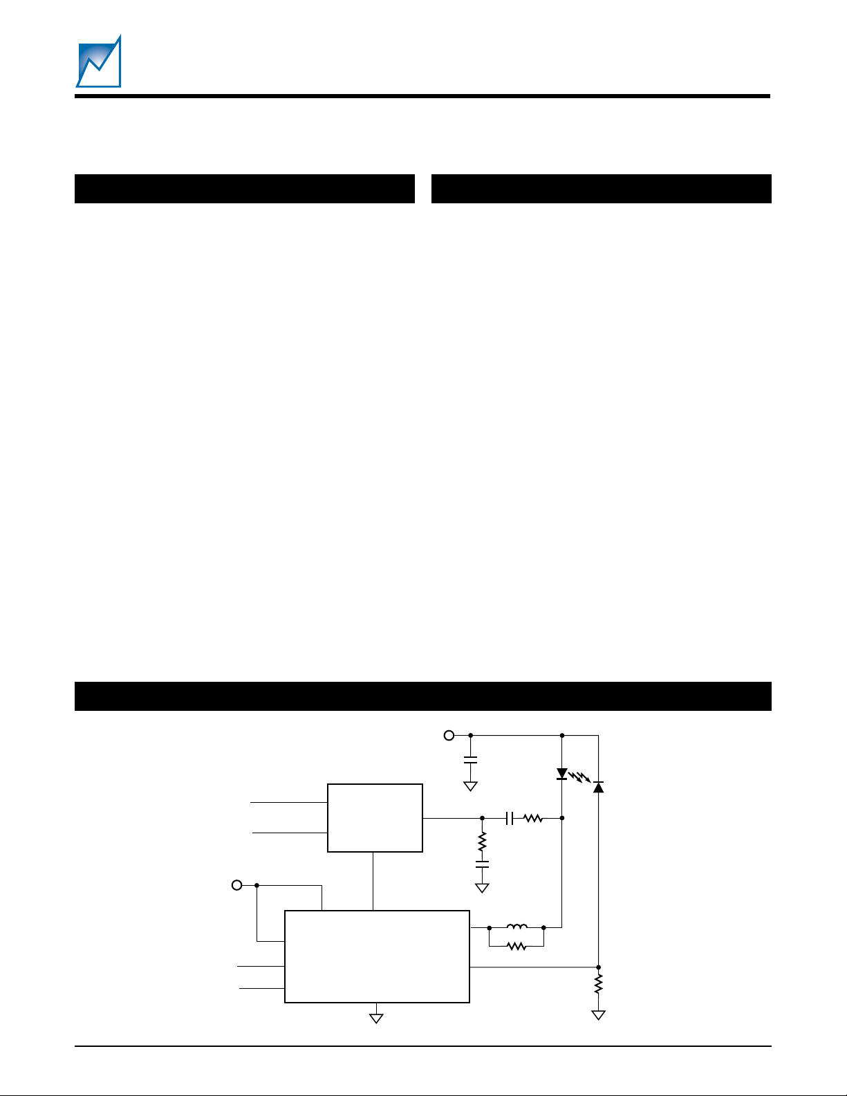
SIMPLIFIED APPLICATION DIAGRAM
V
DD
LASER
IN+
IN–
V
DD
V
AUTOMON
Interface
©SUMMIT MICROELECTRONICS, Inc., 2001 • 300 Orchard City Dr., Suite 131 • Campbell, CA 95008 • Phone 408-378-6461 • FAX 408-378-6586 • www.summitmicro.com
Characteristics subject to change without notice
SDA
SCL
LASER
MODULATION
DRIVER
MODN
DD
SML2108
IMOD
MODSET
BIASN
DETECT
V
SS
2053 3.0 10/03/01
DIODE
MONITOR
DIODE
2053 SAD
1

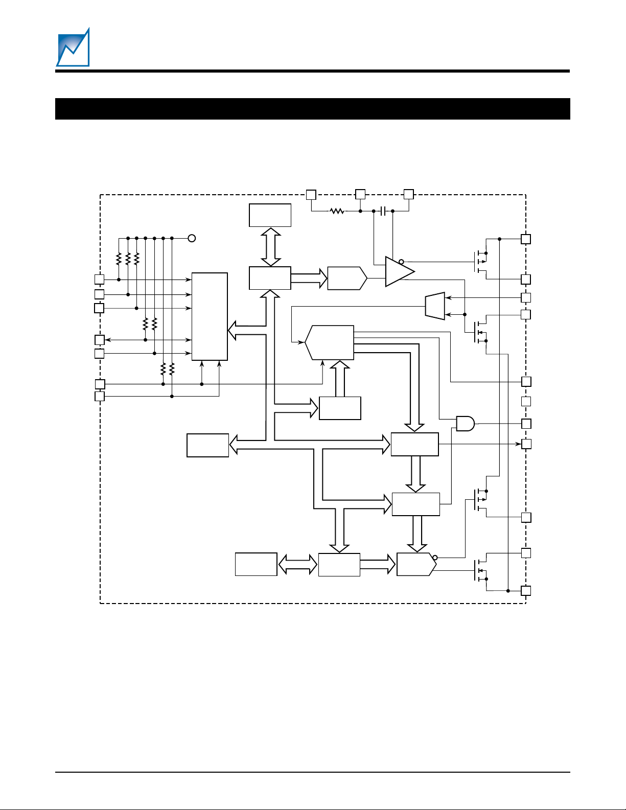
FUNCTIONAL BLOCK DIAGRAM
SML2108
PRELIMINARY
A0
A2
SDA
SCL
AUTOMON
CE#
A1
48
1
2
3
4
5
(All Rs 100kΩ)
6
V
CC
Config
10-Bit
NV Reg
10-Bit
DAC Reg
DETECT
12
10-Bit
DAC
8-Bit
ADC
NV Scaling
& Offset
CAP1
11
CAP2
10
–
+
ADC Read &
Alarm Reg
BIAS P
EXT TEMP
5
BIAS N
13
VSS A
14
VSS D
7
RDY
ALERT#
8
V
DD
NV Look-up
Table
8-Bit
NV Reg
2
2053 3.0 10/03/01
8-Bit
DAC Reg
8-Bit
DAC
2053 BD 2.2
SUMMIT MICROELECTRONICS, Inc.
MOD P
MOD N
V
SS

PIN CONFIGURATION
SML2108
PRELIMINARY
48-Pin TQFP
A0
A1
A2
SDA
SCL
AUTOMON
RDY#
ALERT#
EXT TEMP
CAP2
CAP1
DETECT
CE#
VDDVDDVDDBIASP
BIASP
MODP
MODP
4847464544434241403938
1
2
3
4
5
6
7
8
9
10
11
12
1314151617181920212223
A
D
DDVDD
SS
SS
V
V
V
BIASP
BIASP
MODP
MODP
VDDVDDVSSV
DDVDD
VSSV
V
SS
37
36
35
34
33
32
31
30
29
28
27
26
25
24
SS
MODN
MODN
BIASN
BIASN
V
SS
V
SS
V
SS
V
SS
BIASN
BIASN
MODN
MODN
2053 PCon 2.1
PIN DESCRIPTIONS
DETECT (12)
This is the analog input from the laser monitor photodiode
for the integrator circuit. There is an on-board resistance
of 2MΩ between the DETECT input and CAP1 pin.
CAP1 and CAP2 (11 & 10)
Capacitor inputs for an external capacitor in the feedback
loop of the Mean Power Control Integrator. There is an onboard capacitance of 500pF.
AUTOMON (6)
Active high input used to enable the internal auto-monitor
function, which provides automatic adjustments to the
modulation output currents (MODP and MODN) based on
the internal A/D output and the values stored in the
nonvolatile lookup table. This pin has an internal 100kΩ
pull-up.
SUMMIT MICROELECTRONICS, Inc.
2053 3.0 10/03/01
ALERT# (8)
Active low, open-drain output. This pin is driven low
whenever the bias current increases beyond a predefined
nonvolatile threshold. This can be used to predict laser
failure.
SDA, SCL (4 & 5)
Data and Clock lines, respectively, whose function and
use are based on the industry standard I2C interface.
Lookup table values, configuration data, and D/A and A/D
registers may all be accessed via these two pins of the
SML2108. These pins have internal 100kΩ pull-ups.
A0, A1, A2 (1, 2, & 3)
Address Pins for the interface provided to allow multiple
devices on a single bus. These pins have internal 100kΩ
pull-ups.
3

SML2108
PRELIMINARY
RDY# (7)
Active low, open-drain output. This pin is driven low
whenever the internal A/D is performing a conversion, or
while the on-board EEPROM is being programmed.
EXT TEMP (9)
Temperature input (or no connection). This pin can be
programmed as an input to the ADC and can interface a
temperature sensor. The EXT TEMP pin is multiplexed
with the bias current to provide a means of configuring the
input to the ADC. When EXT TEMP is programmed as the
input to the ADC using bit 5 of Register 1, the converted
value of the current entering this pin is used as the
address of the EEPROM lookup table. In this configuration the modulation current can be controlled by temperature rather than the bias current. Refer to the application
example on using the EXT TEMP pin. If this option is not
used the pin should be left floating.
V
A, VSSD (13 & 14)
SS
Analog and digital low-side supplies for on-board circuitry. Must be at same potential as all other VSS pins.
V
(15, 16, 21, 22, 39, 40, 45, 46, & 47)
DD
High-side supply for the Bias and Modulation currents and
power supply input for the chip.
(23, 24, 29, 30, 31, 32, 37, & 38)
V
SS
Power supply return.
CE# (48)
The chip enable input is active low and provides an
additional method of enabling the serial interface. The
state of this pin has no effect on the auto-monitor function.
This pin has an internal 100kΩ pull-up.
BIASP (17, 18, 43, & 44)
High-side mean bias control current. Current source
output range is programmable, with the optional ranges of
0 to 100mA or 0 to 10mA.
BIASN (27, 28, 33, & 34)
Low-side mean bias control current. Current sink input
range is 0 to 100mA.
MODP (19, 20, 41, &42)
High-side modulation control current. Current source
output range is programmable, with optional ranges of 0 to
100mA or 0 to 10mA.
MODN (25, 26, 35, &36)
Low-side modulation control current. Current sink input
range is 0 to 100mA.
4
2053 3.0 10/03/01
SUMMIT MICROELECTRONICS, Inc.

ABSOLUTE MAXIMUM RATINGS*
SML2108
PRELIMINARY
Temperature Under Bias ...................... –55°C to 125°C
Storage Temperature ........................... –65°C to 150°C
Lead Solder Temperature (10 secs) ................... 300 °C
*COMMENT
Stresses listed under Absolute Maximum Ratings may cause permanent damage to the device. These are stress ratings only, and
functional operation of the device at these or any other conditions
outside those listed in the operational sections of this specification is not
implied. Exposure to any absolute maximum rating for extended
periods may affect device performance and reliability.
ELECTRICAL TABLES
(Over Recommended Operating Conditions; Voltages are relative to GND)
lobmySretemaraPsnoitidnoC.niM.pyT.xaMstinU
ecnamrofrePCDAlacipyT
º
N/SoitaresioNotlangiST
DHTnoitrotsidcinomrahlatoT08– Bd
noitaludomretnicinomrahkaeP
noitrotsid
ycaruccACD
noituloseR8stiB
gnissimonhcihwrofnoituloeR
deetnaraugerasedoc
ycaruccaevitaleR ½±BSL
LND 1±BSL
rorreelacsllufevitisoP2±BSL
V
rorretesfforalopinU
V
º
Cº52= 07Bd
A
redrOdn208– Bd
redrOdr308– Bd
8stiB
V5=2±BSL
SS
SS
V6.3
otV7.2=
2±BSL
2053 Elect Table A
SUMMIT MICROELECTRONICS, Inc.
RECOMMENDED OPERATING CONDITIONS
Temperature –40ºC to 85ºC.
Voltage 3.0V to 5.5V
2053 3.0 10/03/01
5

ELECTRICAL TABLES (Continued)
lobmySretemaraPsnoitidnoC.niM.pyT.xaMstinU
V
DD
I
D
I
OL
I
IL
V
LO
V
HO
V
LI
V
HI
f
TNI
t
SUP
emit
TCETEDCDAottupniTCETED05.1V
I
PMETTXE
I
NDOM
I
PDOM
I
NSAIB
I
PSAIB
V
CAD
tnerruc
tnerruc
TRELAtuptuoTRELA
egatlovylppuS
tnerrucylppuS
tnerrucegakaeltupnIV
NI
tnerrucegakaeltuptuOV
egatlovwoltuptuOI
egatlovhgihtuptuO
LO
V
DD
V
DD
egatlovwoltupnI1.0– 3.0 × V
egatlovhgihtupnI7.0 × V
poolrotargetnI
ycneuqerf
noitazilibatspurewoP
stupnIgolanA
tupnitnerrucelacslluF 6.093Aµ
stuptuOgolanA
noitaludomlennahc-N
noitaludomlennahc-P
tnerrucsaiblennahc-N0001– Am
tnerrucsaiblennahc-P0001Am
tuptuoCADtiB-0105.1V
stuptuOlatigiD
SML2108
PRELIMINARY
noitaludomdnasaibmumixaM
tnerruc
-tuotnerrucnoitaludomdnasaiB
nepostup
VotV0=
DD
TUO
VotV0=
DD
Am2=4.0V
I,V5=
LO
I,V5.4<
LO
Aµ004–=4.2V
Aµ001–=V
sselsitnatsnocemitrotargetnI
sm01naht
situptuoTRELAniardnepO
evitca
35.5V
2Am
1Aµ
01Aµ
2.0– V
DD
V
DD
DD
5.0V
1zHk
01sm
0001– Am
0001Am
5Am
2053 Elect Table B
6
2053 3.0 10/03/01
SUMMIT MICROELECTRONICS, Inc.

DEVICE OPERATION
SML2108
PRELIMINARY
General Description
The SML2108 is an adaptive power controller for laser
diodes with an active feedback loop used to calibrate and
control the mean and modulation power of high speed,
high power laser diodes. Inherent manufacturing tolerances introduce variations of performance in laser diodes.
These variations, combined with parametric changes over
the laser’s extreme temperature range and laser aging,
call for an efficient compensation solution. The SML2108,
with a minimum number of external components, is designed to compensate for these tolerances using a digital
control loop and a programmable nonvolatile calibration
lookup table.
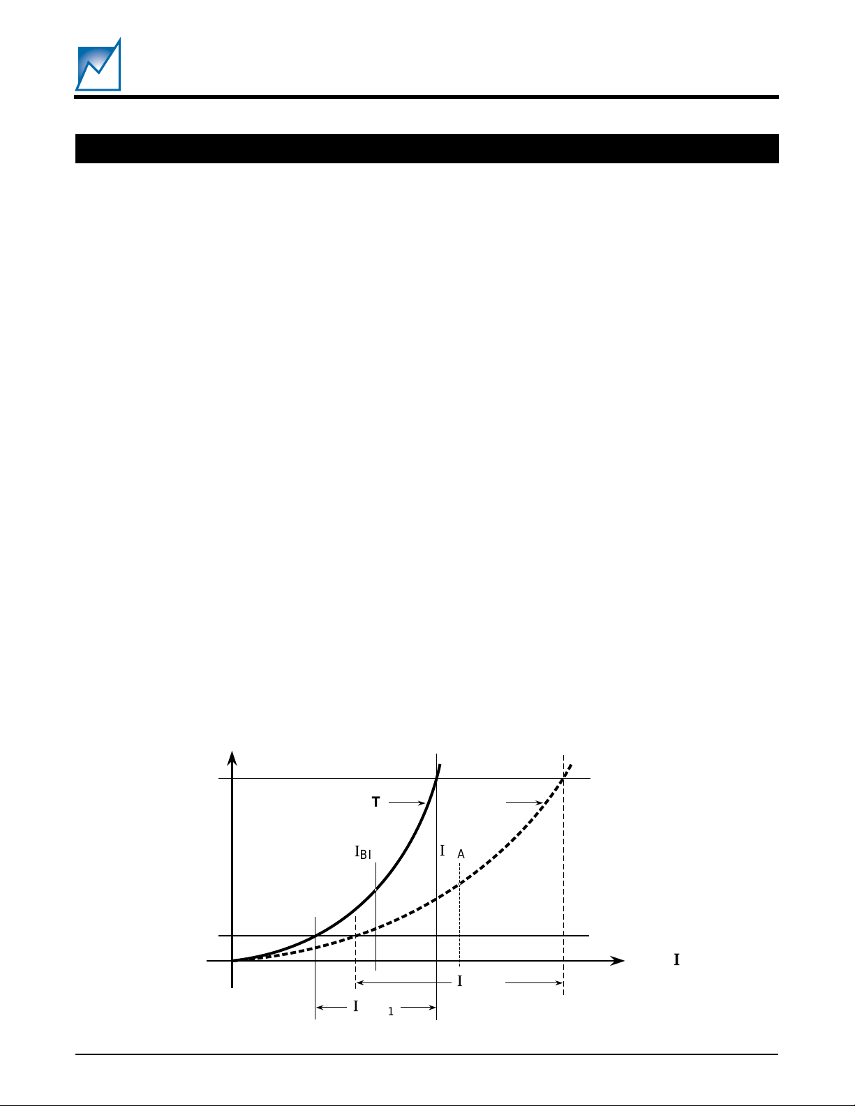
Figure 1 illustrates the usefulness of the SML2108. The
figure shows the output light power of a laser diode versus
its operating current. Depicted in the graph are typical
laser diode characteristics at two different temperatures.
At the first temperature (T
), the laser requires an average
1
bias current of IBIAS1. The modulation current needed to
switch the laser between its on and off state is labeled
IMOD1. The ratio of light power of its on state divided by
the light power of its off state is referred to as the extinction
ratio. Ideally the laser will maintain a constant extinction
ratio over its entire operating temperature range, as the
receiver module is calibrated to this level. Running the
laser driver at a higher extinction ratio indicates that power
is being wasted, whereas operating at a lower extinction
ratio indicates that data may possibly be lost.
The required bias current increases to IBIAS
when the
2
laser is operated at a second temperature (T2). The laser
requires a modulation of IMOD2 to maintain a constant
extinction ratio as in the T1 curve. The SML2108 is the
industry’s first integrated device capable of providing a
variable modulation current based on a function of either
the bias current or an external temperature. This ability
to compensate the modulation output current enables the
system designer to optimize the extinction ratio of the
laser driver module.
The SML2108 has been specified to remove the need for
any manual calibration of the laser control circuit. All
calibration values are programmed through an industry
standard 2-wire communication interface, whose protocol
and function can be controlled by most production ATE
equipment.
Bias Current — Mean Power Control
The SML2108 bias current output (BIASP or BIASN)
establishes the average power being delivered to an
external laser diode. The output of the laser diode is
separately monitored using a local back-face diode, the
output of which is tied to the DETECT pin of the SML2108.
This feedback loop becomes the mean power control for
the laser diode when coupled with the internal integrator.
The output block of the mean power control is shown in
Figure 2.
(On) 1
(Off) 0
Figure 1. Laser Current Increase Caused by Temperature Increase, Constant Light Power Out
SUMMIT MICROELECTRONICS, Inc.
Light
Power
I
BIAS
I
MOD
T1
I
1
1
2053 3.0 10/03/01
BIAS
I
MOD
T2
2
Total
2
2053 Fig01
I
7
 Loading...