SUMMIT
MICROELECTRONICS, Inc.
SMH4811A
Distributed Power Hot-Swap Controller
FEATURES
l Supply Range ±20VDC to >±500VDC
l Versatile Card Insertion Detection Supports:
w Multi-length Pin Systems
w Card Injector Switch Sensing
w Programmable Debounce Periods
l Control Powering-on of DC/DC Converters
l Highly Programmable Host Voltage Monitoring
w Programmable Under- and Over-voltage
Detection
w Programmable UV Filter
l Programmable Power Good Delay for enabling
the DC/DC Converter
l Programmable Circuit Breaker Function
w Programmable Over-Current Filter
w Programmable Quick-Trip™ Circuit Breaker
Values
Preliminary
DESCRIPTION
The SMH4811A is designed to control hot swapping of
plug-in cards operating from a single supply ranging from
20V to 500V. It provides under-voltage and over-voltage
monitoring of the host power supply, drives an external
power MOSFET switch that connects the supply to the
load, and also protects against over-current conditions
that might disrupt the host supply. When the input and
output voltages to its controls are within specification, it
provides a Power Good logic output that may be used to
turn loads on (
or drive a LED status light). Additional features of the
SMH4811A include: temperature sense or master enable
input, 2.5V and 5V reference outputs for expanding monitor functions, two Pin-Detect enable inputs for fault protection, and duty-cycle over-current protection.
e.g.
, an isolated-output DC-DC converter,
l 2.5V and 5.0V reference outputs
w Easy Expansion of External Monitor
Functions
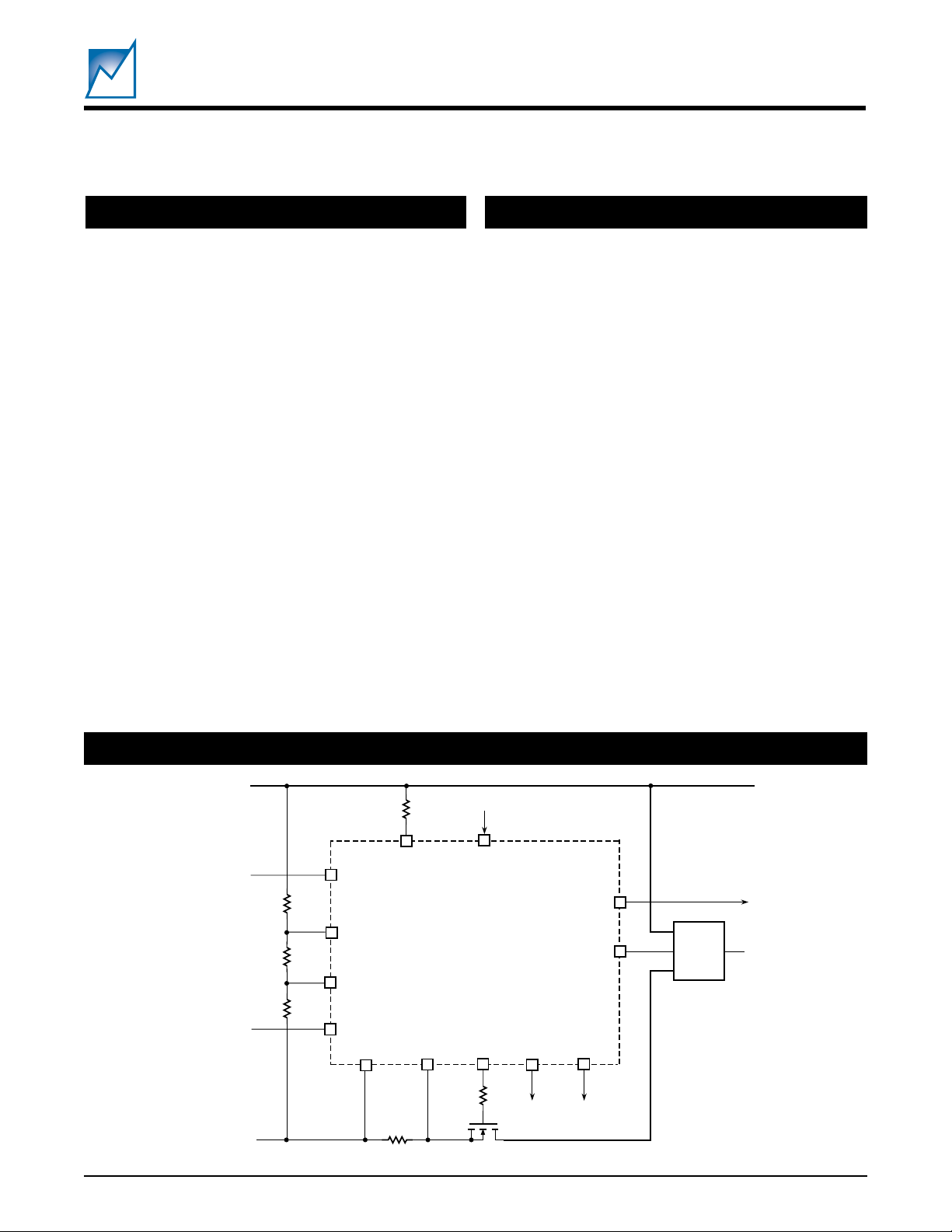
SIMPLIFIED APPLICATION DRAWING
0V
Pin Detect
Pin Detect
PD1#
UV
OV
PD2#
VSS
VDD
CBSENSE
Disable/Enable
ENPG
SMH4811A
VGATE
2.5VREF
FAULT#
PG#
5.0VREF
DC/DC
–48V
©SUMMIT MICROELECTRONICS, Inc., 2000 • 300 Orchard City Dr., Suite 131 • Campbell, CA 95008 • Phone 408-378-6461 • FAX 408-378-6586 • www.summitmicro.com
Characteristics subject to change without notice
2044 6.1 2/8/01
2044 SAD 5.1
1

RECOMMENDED OPERATING CONDITIONS
Temperature –40°C to 85°C.
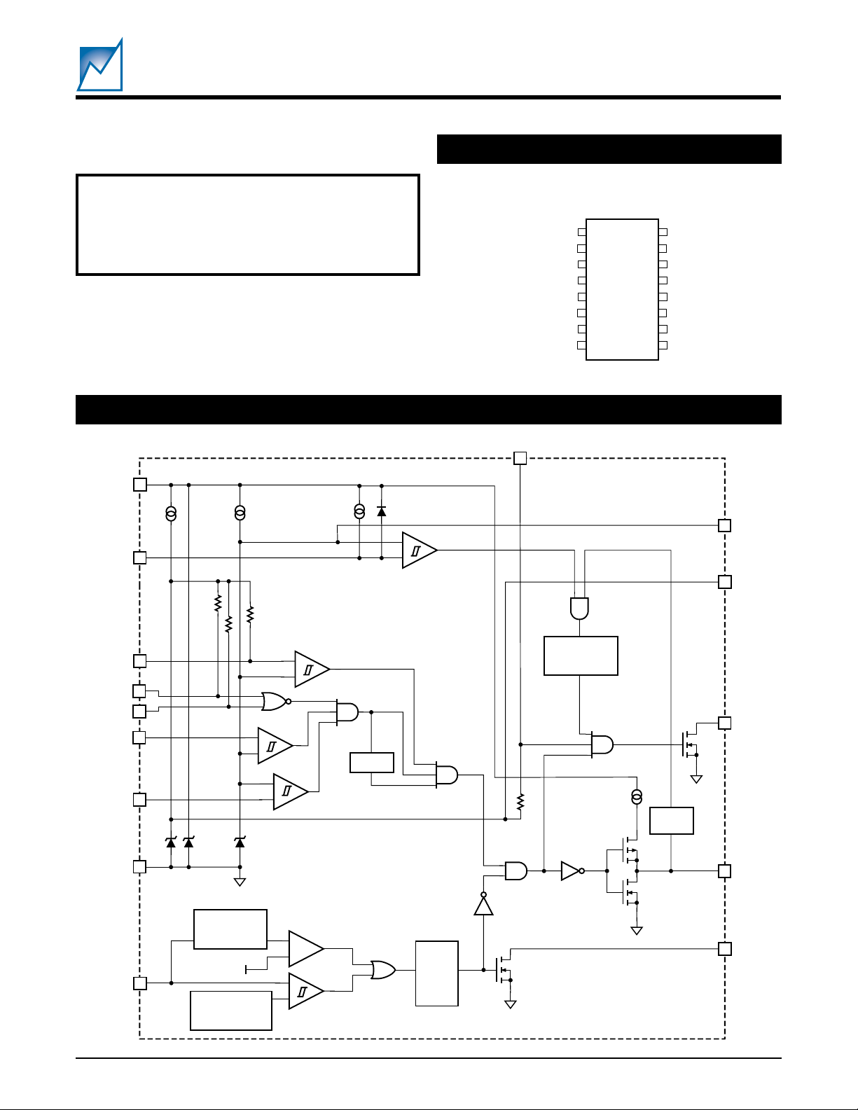
FUNCTIONAL BLOCK DIAGRAM
VDD
16
12VREF
PIN CONFIGURATION
16-Pin SOIC
SS
1
2
3
4
5
6
7
8
DRAIN SENSE
VGATE
EN/TS
PD1#
PD2#
FAULT#
CBSENSE
V
ENPG
14
SMH4811A
Preliminary
V
16
15
14
13
12
11
10
PG#
ENPG
NC
2.5V
5V
OV
UV
9
2044 PCon 5.0
DD
REF
REF
DRAIN
SENSE
EN/TS
PD1#
PD2#
UV
OV
VSS
CBSENSE
12
2.5VREF
+
1
50kΩ
ABLE
50mV
2.5V
200kΩ
+
–
+
–
FILTER
+
–
+
–
+
–
50kΩ
3
4
5
9
10
12V
5V
8
PROGRAMM-
DELAY
7
Programmable
Quick Response
Ref. Voltage
–
DUTY
CYCLE
TIMER
50kΩ
PROGRAMM-
ABLE
DELAY
VGATE
SENSE
11
5.0VREF
15
PG#
2
VGATE
6
FAULT#
2044 BD 5.2
2
2044 6.1 2/8/01
SUMMIT MICROELECTRONICS, Inc.

PIN DESCRIPTIONS
SMH4811A
Preliminary
DRAIN SENSE (1)
The DRAIN SENSE input monitors the voltage at the drain
of the external power MOSFET switch with respect to VSS.
An internal 10µA source pulls the DRAIN SENSE signal
towards the 5V reference level. DRAIN SENSE must be
held below 2.5V to enable the PG outputs.
VGATE (2)
The VGATE output activates an external power MOSFET
switch. This signal supplies a constant current output
(100µA typical), which allows easy adjustment of the
MOSFET turn on slew rate.
EN/TS (3)
The Enable/Temperature Sense input is the master enable input. If EN/TS is less than 2.5V, VGATE will be
disabled. This pin has an internal 200kΩ pull-up to 5V.
PD1# and PD2# (4 & 5)
These are logic level active low inputs that can optionally
be employed to enable VGATE and the PG outputs when
they are at V
. These pins each have an internal 50kΩ
SS
pull-up to 5V.
FAULT# (6)
This is an open-drain, active-low output that indicates the
fault status of the device.
CBSENSE (7)
The circuit breaker sense input is used to detect overcurrent conditions across an external, low value sense
resistor (RS) tied in series with the Power MOSFET. A
voltage drop of greater than 50mV across the resistor for
longer than t
will trip the circuit breaker. A program-
CBD
mable Quick-Trip™ sense point is also available.
OV (10)
The OV pin is used as an over-voltage supply monitor,
typically in conjunction with an external resistor ladder.
VGATE will be disabled if OV is greater than 2.5V. A filter
delay is available on the OV input.
5.0VREF & 2.5VREF (11 & 12)
These are precision 5V and 2.5V output reference voltages that may be use to expand the logic input functions
on the SMH4803A. The reference outputs are with respect to V
SS
.
ENPG (14)
This is an active high input that controls the PG# output.
When ENPG is pulled low the PG# output is immediately
placed in a high impedance state. This pin has an internal
50kΩ pull-up to 5V.
PG# (15)
The PG# pin is an open-drain, active-low output with no
internal pull-up resistor. It can be used to switch a load or
enable a DC/DC converter. PG# is enabled immediately
after VGATE reaches V
– VGT and the DRAIN SENSE
DD
voltage is less than 2.5V. Voltage on these pins cannot
exceed 12V, as referenced to V
SS.
VDD (16)
VDD is the positive supply connection. An internal shunt
regulator limits the voltage on this pin to approximately
12V with respect to VSS. A resistor must be placed in
series with the VDD pin to limit the regulator current (RD in
the application illustrations).
VSS (8)
VSS is connected to the negative side of the supply.
UV (9)
The UV pin is used as an under-voltage supply monitor,
typically in conjunction with an external resistor ladder.
VGATE will be disabled if UV is less than 2.5V. Programmable internal hysteresis is available on the UV input,
adjustable in increments of 62.5mV. Also available is a
filter delay on the UV input.
SUMMIT MICROELECTRONICS, Inc.
2044 6.1 2/8/01
3

ABSOLUTE MAXIMUM RATINGS*
SMH4811A
Preliminary
Temperature Under Bias ...................... –55°C to 125°C
Storage Temperature ........................... –65°C to 150°C
Lead Solder Temperature (10 secs) ................... 300 °C
Terminal Voltage with Respect to VSS:
V
................................. –0.5V to V
DD
DD
OV, UV, DRAIN SENSE,
CBSENSE...........–0.5V to VDD+0.5V
PD1#, PD2#, ENPG, EN/TS ......... 10V
FAULT#, PG# ........–0.5V to VDD+0.5V
VGATE ................................ VDD+0.5V
AC OPERATING CHARACTERISTICS
lobmySnoitpircseD.niM.pyT.xaMstinU
t
DBC
t
DGP
t
NDTHSTSF
t
CYC
t
FVUP
t
DDP
Note: * Indicates default value
)retlif(yaleDrekaerBtiucriCVm05
yaleDdooGrewoPelbammargorP
emitedomelcycrekaerbtiucriC *5.2s
retlifegatloV-rednUelbammargorP
yaleDtceteDniPelbammargorP
*COMMENT
Stresses listed under Absolute Maximum Ratings may cause permanent damage to the device. These are stress ratings only, and
functional operation of the device at these or any other conditions
outside those listed in the operational sections of this specification is not
implied. Exposure to any absolute maximum rating for extended
periods may affect device performance and reliability.
004sµ
051sµ
*05sµ
5sµ
05sµ
052sµ
005sµ
5.1sm
*5sm
02sm
08sm
061sm
ffoETAGVottluafmorfyalednwoDtuhStsaF 002sn
*ffO —
5sm
08sm
061sm
5.0sm
5sm
*08sm
061sm
2044 Prog Table
4
2044 6.1 2/8/01
SUMMIT MICROELECTRONICS, Inc.

DC OPERATING CHARACTERISTICS
(Over Recommended Operating Conditions; Voltages are relative to VSS)
lobmySretemaraPsnoitidnoC.niM.pyT.xaMstinU
V
DD
FERV0.5tuptuoecnereferV5I
I
5DAOL
FERV5.2tuptuoecnereferV5.2
I
5.2DAOL
I
DD
V
VU
V
TSYHVU
V
VO
V
TSYHVO
V
ETAGV
I
ETAGV
V
ESNES
I
ESNES
V
BC
V
BCQ
V
STNE
V
V
V
V
V
Note: (1) TA = 25ºC.
TSYHSTNE
HI
LI
LO
TG
egatlovylppuSI
tnerructuptuoecnereferV5I
I
I
tnerructuptuoecnereferV5.2I
tnerrucylppusrewoPdelbanetuptuO2 01Am
I
dlohserhtegatloV-rednU
I
siseretsyhegatloV-rednUI
I
dlohserhtegatloV-revO
I
siseretsyhegatloV-revOI
egatlovtuptuoETAGV V
tuptuotnerrucETAGV001Aµ
I
dlohserhtESNESNIARD
I
tuptuotnerrucESNESNIARDV
dlohserhtrekaerbtiucriCI
tiucricpirTkciuQelbammargorP
dlohserhtrekaerb
I
dlohserhtST/NE
I
siseretsyhST/NEI
GPNE:egatlovhgihtupnI2FERV0.5V
GPNE:egatlovwoltupnI1.0– 8.0V
#TLUAF:egatlovwoltuptuOI
#GP:egatlovwoltuptuOI
dlohserhtetaG7.08.10.3V
Am3=112131V
DD
Am3=57.400.552.5V
DD
Am3=1– 1Am
DD
Am3=)1(574.2005.2525.2V
DD
Am3=524.2005.2575.2V
DD
Am3=2.0– 1Am
DD
Am3=)1(574.2005.2525.2V
DD
Am3=524.2005.2575.2V
DD
Am3=01Vm
DD
Am3=)1(574.2005.2525.2V
DD
Am3=524.2005.2575.2V
DD
Am3=01Vm
DD
Am3=)1(574.2005.2525.2V
DD
Am3=524.2005.2575.2V
DD
V=
ESNES
DD
)1(9 0111Aµ
SS
Am3=040506Vm
ffO —
Am3=)1(574.2005.2525.2V
DD
Am3=524.2005.2575.2V
DD
Am3=01Vm
DD
Am2=0 4.0V
LO
Am2=0 4.0V
KNIS
SMH4811A
Preliminary
DD
002Vm
001Vm
06Vm
2044 Elect Table
V
SUMMIT MICROELECTRONICS, Inc.
2044 6.1 2/8/01
5
 Loading...