

Page 1

CPMC-1553R
User’s Guide
Page 2

CPMC-1553R
User’s Guide
CA.DT.356-0e MARCH, 2002
Page 3

Corporate Headquarters
150, rue Marcellin Berthelot
ZI Toulon-Est BP 244
83078 TOULON Cedex 9
France
Tel : +33 - (0) 4 94 16 34 00
Fax : +33 - (0) 4 94 16 34 01
USA Headquarters
1203 New Hope Road
Raleigh - NC 27610
USA
Tel : +1 - (800) 848 2330
Tel : +1 - (919) 231 8000
Fax : +1 - (919) 231 8001
International Sales
Department
67, rue du Charles De-Gaulle
78350 JOUY-EN-JOSAS
France
Tel : +33 - (0) 1 39 56 72 72
Fax : +33 - (0) 1 39 56 72 70
United Kingdom
Cornwell Business Park
31 Salthouse Road Brackmills
Northampton D NN4 7EX
United Kingdom
Tel : +44 - (0) 1604 700 221
Fax : +44 - (0) 1604 700 112
www.thalescomputers.com
Thales Computers, The Ruggedizer, UNI/RT and POWERENGINE are registered trademarks of Thales
Computers S.A. - PowerPC, AIX, AIXwindows, RISC System/6000, IBM are registered trademarks of IBM
Corp. - LynxOS is a registered trademark of LynuxWorks, Inc. - TORNADO and VxWorks are registered
trademarks of Wind River System, Inc. - UNIX is a registered trademark licensed exclusively by X/Open
Company Limited. - All other product names, trademarks and registered trademark are the property of
their respective holders.
Copyright Thales Computers 1987 - 2002
Thales Computers reserves the right to ma ke chan ges furthe r notice t o any pro ducts her ein, Tha les Comp uters make s no warra nty, representation or
guarantee regarding the suitability of its products for any particular purpose, nor does Thales Computers assume any liability arising out of the
application or user of any product or c ircuit, and specifically disclaims any and all liabilit y, including without limitation consequential or incidental
damages. “Typical” parameters can and do vary in different applications. All operating parameters including “Typicals” must be validated for each
customer application by customer’s technical experts. Thales Computers does not convey any license under its patent rights nor the rights others. Thales
Computers products are not designed, intended, or authorized for use as components in systems intended for surgical implant into body, or other
applications intended to support or sustain life, or for any other application in which the failure of the Thales Computers product could create a situation
where personal injury or death may occur. Should Buyer purchase or use Thales Computers products for any such unintended or unauthorized
application, Buyer shall indemnify and hold Thales Co mputers and its officers, employees, subsidiaries, affiliates, and distributors harmless against all
claims, costs, damages, and expenses, and reasonable attorney fees arising out of, directly or indirectly, any claim of personal injury or death associated
with such unintended or unauthorized use, even if such claim alleges that Thales Computers was negligent regarding the design or manufacture of the
part.
Restricted Rights Legend
Use, duplication or disclosure by the contractor or the Government is subject to restrictions as set forth in subdivision (b) (3)(ii) of the Rights in Technical
Data and Computer Software clause 52.227-7013.
No communication, reproduction or use without prior written approval from Thales Computers
Your comments on this manual will be welcome.
A sheet is appe nded for you to submit your rema rks.
Page 4

Table of Contents
Chapter 1 Introduction................................................................................................................................1-1
1.1 Manual Overview.......................................................................................................................1-1
1.2 CPMC-1553R Features..............................................................................................................1-2
1.3 CPMC-1553R Options...............................................................................................................1-3
1.4 Installation and Configuration....................................................................................................1-3
1.4.1 Precautions ....................................................................................................................1-3
1.4.2 Installation.....................................................................................................................1-3
Chapter 2 Operation................................................................................................................................2-1
2.1 Functional Description ...................................................................................................... ......... 2-1
2.2 PCI Bus Interface.......................................................................................................................2-2
2.2.1 PCI Configuration Space...............................................................................................2-2
2.2.2 PCI Memory Space........................................................................................................2-6
2.2.3 PCI I/O Space..............................................................................................................2-11
2.2.4 Interrupt A (INTA*).................................................................................................... 2-11
2.3 MIL-STD-1553B Bus..............................................................................................................2-11
2.3.1 Signal Naming Convention .........................................................................................2-11
2.3.2 Remote Terminal Address...........................................................................................2-11
2.4 Power Requirements................................................................................................................2-13
Appendix A List of Abbreviations......................................................................................................... A-1
List of Tables
Table 1. Industry Specifications and Standards.......................................................................................1-1
Table 2 PCI Bus Configuration Registers...............................................................................................2-2
Table 3 Summary of Implemented PCI Configuration Registers............................................................2-3
Table 4 Command Register Definition ...................................................................................................2-3
Table 5 Status Register Definition..........................................................................................................2-4
Table 6 Memory Base Address Registers Definitions............................................................................2-5
Table 7 Mapping of PCI Memory Space to ACE Internal Registers......................................................2-7
Table 8 Signal Definition of ACE Configuration Register.....................................................................2-9
Table 9 Interrupt Control/Status Register ...............................................................................................2-9
Table 10 ACE Memory Space Address Mapping...................................................................................2-10
Table 11 Pn4 Signal Definitions.............................................................................................................2-12
Table 12 Power Requirements................................................................................................................2-13
Thales Computers - i - CPMC-1553R User’s Guide, CA.DT.356-0e
Page 5

Chapter 1 −−−− Introduction
1.1 Manual Overview
This manual describes the CPMC-1553R board from Thales Computers. Chapter 1 summarizes the board’s
features and provides installation instructions. Chapter 2 describes its functional characteristics. Appendix
A is a list of the abbreviations used in this manual.
This manual uses the following terminology conventions:
• Addresses and signal names are shown in capital letters.
• An asterisk* after a signal name indicates active low.
• Hexadecimal notation is indicated by the prefix 0x.
Thales Computers products are designed to meet several industry specifications and standards. Board
installers and operators should be familiar with the concepts of these documents.
Table 1. Industry Specifications and User Documentation
Category Document Ordering Information
PCI Local Bus PCI Local Bus Specification,
Rev. 2.1, June 1, 1995
PMC Draft Standard Physical and
Environmental Layers for PCI Mezzanine
Cards: PMC, P1386.1/Draft 2.0, 5/4/95
MIL-STD1553B Bus
FLEX 10K
PLD
MIL-STD-1553 Designer’s Guide,
Fifth Edition,
BU-65170/61580 and BU-61585
ACE Series BC/RT/MT Advanced
Communication Engine Integrated 1553
Terminal BU-65170, BU-61580,
BU-61590, BU-65178,BU- 615 88,
BU-61582, BU61583, BU-65620, and
BU-65621 User’s Guide, Rev. G
BU-65178/65179*/61588/61688*/61689*
Miniature Ad va nce d Co mmuni c at io n s
Engine (Mini-ACE) and Mini-ACE
Plus*, BU-61688
Altera Flex 10K
Altera Data Book, 1998
PCI Special Interest Group
P.O. Box 14070
Portland, OR 97214
(800)433-5177
IEEE Standards Department
Order Department
445 Hoes Lane,
P.O. Box 1331
Piscataway, NJ 08855-1331
ILC Data Device Corporation
105 Wilbur Place
Bohemia, NY 11716
(516)567-5600
Altera Corporation
101 Innovation Drive
San Jose, CA 95134
(408)544-7000
Thales Computers 1-1 CPMC-1553R User’s Guide, CA.DT.356-0e
Page 6
1.2 CPMC-1553R Features
The CPMC-1553R is a single, conduction-cooled, PMC card with two dual-redundant MIL-STD-1553
Buses. The card has the following features:
• Two ILC-DDC BU-61688 Mini-ACE MIL-STD-1553 interface devices (single version available)
- 64kBx16 shared RAM
- Fully integrated MIL-STD1553 A/B
- Bus Controller (BC)/ Remote Terminal (RT)/Monitor Terminal (MT) configurable through
software
- Direct or transformer coupled interfaces
- Internal time tag register
- Interrupt status register
• Bus controller features
- Automatic retries
- Programmable intermessage gap times
- Automatic frame repetition
- Flexible interrupt generation
• RT features
- RT address selected via PMC connector
- Full software control of RT Status and Built-in-Test (BIT) words
- Double buffer and circular buffer options programmable by subaddresses
- Internal command illegalization
• MT features three modes – word monitor, selective message monitor, and a combined RT/selective
monitor
• PCI interface
- 33 MHz, 32-bit, 5V or 3.3V PCI bus
- Interrupt on INTA*
• Eight TTL-level user inputs
• Eight TTL-level user outputs – open-drain output drivers
• Temperature range -40 - +85°F
• Weight – 96 grams
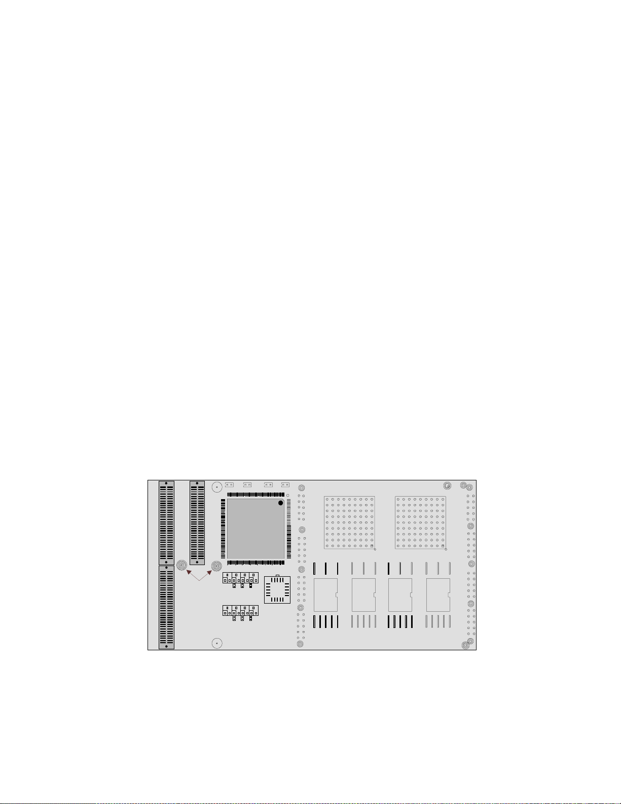
22
1
2
1
P12
22
P11
1
3.3V or 5.0 V
Keying
P14
D4 D3 D2
D8 D7 D6
Altera
FLEX10
D1
D5
ILC-DDC
Mini-ACE
ILC-DDC
Mini-ACE
Figure 1. CPMC-1553R Board Layout
Thales Computers 1-2 CPMC-1553R User’s Guide, CA.DT.356-0e
Page 7

1.3 CPMC-1553R Options
Figure 2 shows the standard options available for the CPMC-1553R.
CPMC-1553R-__ __
Environment
Industrial/-SA.................................................................................I
Rugged/-RA....................................................................................R
Militarized/-RC ..............................................................................M
Channels
1 Channel..............................................................................................1
2 Channels............................................................................................2
Figure 2. CPMC-1553R Standard Options
1.4 Installation and Configuration
1.4.1 Precautions
Electrostatic discharge can damage many of the components of the CPMC-1553R. Therefore, it should be
kept in its protective antistatic bag until it is ready to be configured and installed. During installation or
whenever the CPMC-1553R is removed from the bag, it is important to follow proper grounding
procedures. Such procedures include use of an antistatic workstation, an operator wrist strap, and a
grounded bench mat. Save the antistatic bag for use in storing or shipping the CPMC-1553R.
Closely inspect the board for any signs of shipment-related damages such as loose components or bent pins.
If any evidence of damage is discovered, please notify the carrier and Thales Computers immediately.
1.4.2 Installation
The CPMC-1553R board attaches to a PMC carrier board. The attaching hardware for the CPMC-1553R
board is included with your order.
Attach the CPMC-1553R board to the PMC carrier board according to the following instructions.
a. Remove the PMC carrier board from the chassis.
b. Align the PCI connectors on the component side of the CPMC-1553R board with the PCI connectors
on the component side of the PMC carrier board. Press them together so that the friction from the pins
holds them together. After inserting the board make sure that the connectors have not shifted.
c. Insert the screws supp lied with the board , through the botto m of the PMC carrier b oard and into the
standoffs attached to the CPMC-1553R.
d. For a conduction-cooled board, install the remaining screws through the CPMC-1553R into the
reinforcing bars on the PMC carrier board.
e. Insert the PMC carrier board back into the chassis making sure it is plugged into the backplane.
f. Turn on the system power.
Thales Computers 1-3 CPMC-1553R User’s Guide, CA.DT.356-0e
Page 8

Chapter 2 −−−− Operation
2.1 Functional Description
The CPMC-1553R is a PMC card with one or two, dual-redundant MIL-STD-1553B buses, eight user
inputs, and eight user outputs. The board interfaces to the user I/O through the PMC connector Pn4. Two
PMC connectors, Pn1 and Pn2 provide a direct connection to the PCI Bus. The Altera FLEX10
Programmable Logic Device (PLD) and the ILC-DDC Mini-ACE Device provide the interface between the
PCI bus and the MIL-STD-1553B bus. Each MIL-STD-1553B bus is implemented using an ILC-DDC
Mini-ACE device with 64kB x 16 of shared RAM. The implementation is shown in Figure 3.
Pn1 Pn2
PCI Bus
PCI Interface
(Altera PLD)
User Inputs
User Outputs
Figure 3. CPMC-1553R Implementation Diagram
Local Bus Signals
1553 Interface
(ILC-DDC
Mini-ACE Devices)
MIL-STD-1553_1 TX/RX Channel A/B
MIL-STD-1553_1 RT address
MIL-STD-1553_2 TX/RX Channel A/B
MIL-STD-1553_2 RT address
Pn4
9903-1
Thales Computers 2-1 CPMC-1553R User’s Guide, CA.DT.356-0e
Page 9
2.2 PCI Bus Interface
An Altera FLEX10 PLD provides the interface between the PCI Bus and the ILC-DDC Mini-ACE device.
The FLEX10 operates at 33MHz, is powered by 5V or 3.3V, has a 32-bit data path, and is compliant with
the PCI Local Bus Specification, Revision 2.1. The CPMC-1553R is a target on the PCI Bus.
2.2.1 PCI Configuration Space
The PCI configuration space consists of a block of 64 configuration DWORDS, of which, the first 16 are
defined by the PCI Special Interest Group (PCI SIG). The configuration space defined by PCI SIG is
shown in Table 2. The shaded areas indicate registers that are supported by the CPMC-1553R board. A
summary of the supported configuration registers, and their default values is shown in Table 3. Any
registers that are not supported return a value of 0x00 when read.
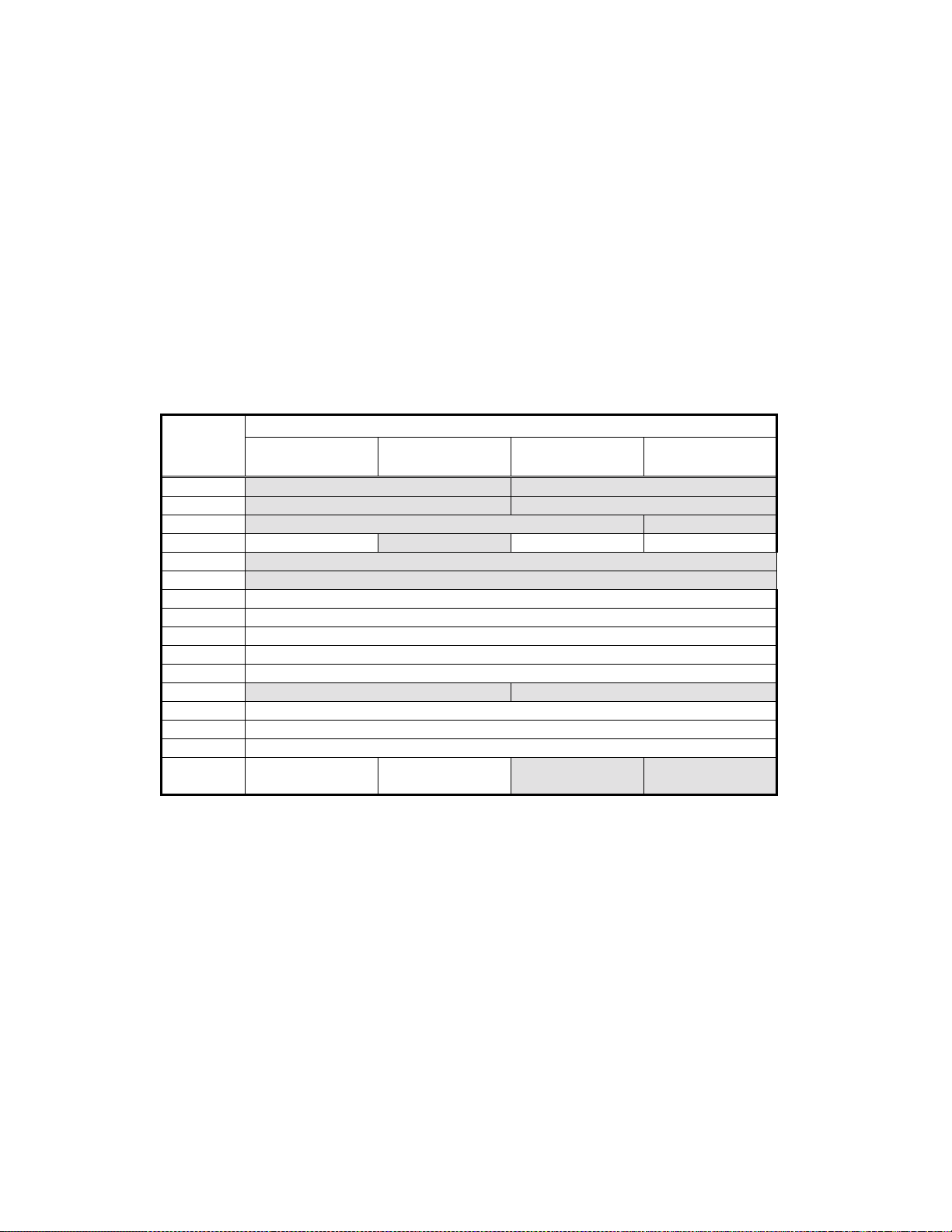
Table 2. PCI Bus Configuratio n Registers
Byte
Address
(0x)
00 Device ID Vendor ID
04 Status Register Command Register
08 Class Code Revision ID
0C BIST Header Type Latency Timer Cache Line Size
10 Base Address Re gister 0
14 Base Address Re gister 1
18 Base Addre ss Register 2
1C Base Address Register 3
20 Base Addre ss Register 4
24 Base Addre ss Register 5
28 Card Bus CIS Pointer
2C Subsystem ID Subsystem Vendor ID
30 Expansion ROM Base Address Register
34 Reserved
38 Reserved
3C Maximum
3210
Latency
Minimum Grant
Interrupt Pin Interrupt Line
Thales Computers 2-2 CPMC-1553R User’s Guide, CA.DT.356-0e
Page 10

Table 3. Summary of Implemented PCI Co nfiguration Registers
Register Name
Address
(0x)
Read/Write
Default Value
(0x)
Vendor ID 00 Read 151E
Device ID 02 Read 0001
Command Register 04 Read/Write 0000
Status Register 06 Read/Write 0400
Revision ID 08 Read 03 or higher
Class Code 09 Read 078000
Header Type 0E Read 00
Base Address Register 0 10 Read/Write FFFC0000
Base Address Register 1 14 Read/Write FFFFF000
Subsystem Vendor ID 2C Read 151E
Subsystem ID 2E Read 0001
Interrupt Line 3C Read/Write 00
Interrupt Pin 3D Read 01
2.2.1.1 Vendor ID Register The Vendor ID is a 16-bit register assigned to Thales Computers that
identifies the manufacturer of the device. The value of this register should always be 0x151E.
2.2.1.2 Device ID Register The Device ID is a 16-bit read-only register assigned by Cetia that identifies
the PCI interface device. The value of this register should always be 0x0001.
2.2.1.3 Command Register The Command Register is a 16-bit read/write register that provides basic
control over the ability of the CPMC-1553R board to respond to the PCI bus. The Command Register is
defined in Table 4. The default value of the Command Register is 0x0000.
Table 4. Command Register Definition
Data
Bit
0 IO_ENA Read/Write Read/write to I/O access enable.
1 MEM_ENA Read/Write Memory Access Enable. When high, MEM_ENA
5..2 Unused — —
6 PERR_ENA Read/Write Parity Error Enable. When high, PERR_ENA
7Unused — —
8 SERR_ENA Read/Write System Error Enable. When high, SERR_ENA
15..9 Unused — —
Mnemonic Read/Write Definition
allows the CPMC-1553R to respond to PCI Bus
memory accesses.
enables the CPMC-1553R to report parity errors via
the PERR* output.
allows the CPMC-1553R to report address parity
errors via the SERR* output. However, to signal a
system error, the PERR_ENA bit mu st also be high.
Thales Computers 2-3 CPMC-1553R User’s Guide, CA.DT.356-0e
Page 11

2.2.1.4 Status Register The Status Register is a 16-bit read/write register that provides the status of bus-
related events. Read transactions tell you the current status of the bits. The Status Register is cleared by
writing a logic one to that bit. Writing a logic zero has no affect on the registers. The status register is
defined in Table 5. The default value of the status register is 0x0400.
Table 5. Status Register Definition
Data Bit Mnemonic Read/Write Definition
8..0 Unused
——
10..9 DEVSEL_TIM Read Device Select Timing. The DEVSEL_TIM bits
indicate target access timing of the CPMC-1553R
board function. This board function is designed to be
a slow target device. These bits are always read as
0x10b.
11 TABORT_SIG Read/Write Target Abort Signaled. This bit is set when a local
peripheral device terminates a transaction. The
CPMC-1553R board automatically sets this bit if it
issued a target abort after the local side asserted
LT_ABORT*. This bit is driven to the local side on
the TABORT_SIG output.
12 TAR_ABRT_REC Read/Write Targe t Ab ort. When high, TAR_ABRT_REC
indicates that the current target device transaction has
been terminated.
13 Unused
——
14 SERR_ SET Read/Write Signaled System Error. When high, SERR_SET
indicates that the CPMC-1553R board drove the
SERR* output active (result of address phase parity
error). This signal is driven to the local side on the
SERR_SIG output
15 DET_PAR_ERR Read/Write Detected Parity Error. When high, DET_PAR_ERR
indicates that the CPMC-1553R board detected either
an address or data parity error. Even if parity error
reporting is disabled (PERR_ENA), the CPMC-1553R
board sets the DET_PAR_ERR bit. This signal is
driven to the local side on the PERR_DET output.
2.2.1.5 Revision ID Register The Revision ID register is an 8-bit, read-only register that identifies the
revision number of the device. The value of this register is set by Thales Computers. The current version
should be 0x03 or higher.
2.2.1.6 Class Code Register The Class Code register is a 24-bit, read-only register divided into three
sub-registers: base class, sub-class, and programming interface. The class code register always returns a
value of 0x078000 when read.
2.2.1.7 Cache Line Size Register The Cache Line Size register is not supported.
Thales Computers 2-4 CPMC-1553R User’s Guide, CA.DT.356-0e
Page 12

2.2.1.8 Latency Timer Register The Latency Timer register is not supported.
2.2.1.9 Header Type Register The Header Type register is an 8-bit, read-only register that identifies the
CPMC-1553R board as a single function device. This register returns a value of 0x00 when read.
2.2.1.10 Built-In Self Test Register The Built-In Self Test (BIST) Register is not supported.
2.2.1.11 Base Address Registers Each of the six Base Address Registers (BAR#) has identical attributes.
Each BAR should be a 32-bit Hexadecimal number, that selects a combination of the followin g options:
type of address space, location of the reserved memory in the 32-bit address space, sets the reserved
memory as prefetchable or non-prefetchable, and the size of memory or I/O address space reserved for the
BAR.
BAR0 is a read/write register that is used for the CPMC-1553R Memory Base Address Register. After
writing 0xFFFFFFFF to this register, reading this register will return the value 0xFFFC0000.
BAR1 is a read/write register that is used for the CPMC-1553R Register Base Address Register. After
writing 0xFFFFFFFF to this register, reading this register will return the value 0xFFFFF000.
BAR2-BAR5 are unused. These registers return the value of 0x0000 when read.
Table 6. Memory Base Address Registers Definitions
Data
Bit
Mnemonic Read/Write Definition
0 MEM_IND Read Memory indicator.
0 – register maps into memory address space
1 – register maps into I/O address space
2..1 MEM_TYPE Read Memory type
00 – locate anywhere in 32-bit address space
01 – locate below 1MB
10 – locate anywhere in 64-bit address space
11 - reserved
3 PRE_FETCH Read/write Memory prefetchable. The PRE_FETCH bit indicates
whether the blocks of memory are prefetchable by the
host bridge.
31..4 BAR Rea d/write Base address register
2.2.1.12 Card Bus CIS Pointer Register The Card Bus Card Information Structure (CIS) Pointer Register
is not supported.
2.2.1.13 Subsystem Vendor ID Register The Subsystem Vendor ID register is a 16-bit, read-only
register that identifies Thales Computers as the vendor for the CPMC-1553R card. The value of this
register should always be 0x151E.
2.2.1.14 Subsystem ID Register T he Subsystem ID Register is a 16-bit, read-only register that identifies
the CPMC-1553R board. The value of this register should always be 0x0001.
Thales Computers 2-5 CPMC-1553R User’s Guide, CA.DT.356-0e
Page 13

2.2.1.15 Expansion ROM Base Address Register The Expansion ROM Base Add ress Register is not
supported.
2.2.1.16 Interrupt Line Register The Interrupt Line Register is an 8-bit, read/write register that defines
which system interrupt request line (on the system interrupt controller) the INTA* output is routed. The
default value for this register is 0x00.
2.2.1.17 Interrupt Pin Register The Interrup t Pi n Regist er is an 8 -bit, re ad-o nly re giste r t hat d e fine s t he
PCI interrupt generated by this board to be INTA*. This register returns a value of 0x01 when read.
2.2.1.18 Minimum Grant Register The minimum Grant Register is not supported.
2.2.1.19 Maximum Latency Register The Maximum Latency Register is not supported.
2.2.2 PCI Memory Space
The ACE registers, user defined discrete I/O, and ACE memory are all mapped to the PCI memory space.
2.2.2.1 ACE Register Space The ACE register space is mapped into the PCI memory space. The
location of the ACE register and user defined discrete I/O is defined in Base Address Register 1 (BAR1),
address 0x14 in PCI configuration space. This space provides the software interface to the ACE device via
17 internal operational registers. The mapping of these registers is defined in Table 7. For more
information regarding the function of the register space of the ACE device, refer to the ILC-DDC data
sheet for BU-61688.
Thales Computers 2-6 CPMC-1553R User’s Guide, CA.DT.356-0e
Page 14

Table 7. Mapping of PCI Memory Space to ACE Internal Registers
PCI Address
(AD15..AD0)
ACE Address
(ADDR15..ADDR0)
Read/Write Description
0000 0000 Read/Write ACE#1 – Interrupt Mask Register
0002 0001 Read/Write ACE#1 – Configuration Register #1
0004 0002 Read/Write ACE#1 – Configuration Register #2
0006 0003 Write
ACE#1 – Start/Reset Register
Read
ACE#1 – BC/RT Command Stack Pointer
Register
0008 0004 Read/Write ACE#1 – BC Control Word Register/RT
Subaddress Control Word Register
000A 0005 Read/Write ACE#1 – Time Tag Register
000C 0006 Read ACE#1 – Interrupt Status Register
000E 0007 Read/Write ACE#1 – Configuration Register #3
0010 0008 Read/Write ACE#1 – Configuration Register #4
0012 0009 Read/Write ACE#1 – Configuration Register #5
0014 000A Read/Write ACE#1 –Data Stack Address Register
0016 000B Read ACE#1 – BC Frame Time Remaining
Register
0018 000C Read ACE#1 – BC Message Time Remaining
Register
001A 000D Read/Write ACE#1 – BC Frame Time/RT Last
Command/MT Trigger Register
001C 000E Read ACE#1 – RT Status Word Register
001E 000F Read ACE#1 – RT BIT Word Register
0020 0010 Read/Write ACE#1 – Test Mode Register 0
0022 0011 Read/Write ACE#1 – Test Mode Register 1
0024 0012 Read/Write ACE#1 – Test Mode Register 2
0026 0013 Read/Write ACE#1 – Test Mode Register 3
0028 0014 Read/Write ACE#1 – Test Mode Register 4
002A 0015 Read/Write ACE#1 – Test Mode Register 5
002C 0016 Read/Write ACE#1 – Test Mode Register 6
002E 0017 Read/Write ACE#1 – Test Mode Register 7
0030 0018 Read/Write ACE#1 – Reserved
0032 0019 Read/Write ACE#1 – Reserved
0034 001A Read/Write ACE#1 – Reserved
0036 001B Read/Write ACE#1 – Reserved
0038 001C Read/Write ACE#1 – Reserved
003A 001D Read/Write ACE#1 – Reserved
003C 001E Read/Write ACE#1 – Reserved
003E 001F Read/Write ACE#1 – Reserved
0040 – 007F — — ACE#1 – Reserved for Future Expansion
Thales Computers 2-7 CPMC-1553R User’s Guide, CA.DT.356-0e
Page 15

Table 7. Mapping of PCI Memory Space to ACE Internal Registers - Continued
PCI Address
(AD15..AD0)
ACE Address
(ADDR15..ADDR0)
Read/Write Description
0080 0000 Read/Write ACE#2 – Interrupt Mask Register
0082 0001 Read/Write ACE#2 – Configuration Register #1
0084 0002 Read/Write ACE#2 – Configuration Register #2
0086 0003 Write
ACE#2 – Start/Reset Register
Read
ACE#2 – BC/RT Command Stack Pointer
Register
0088 0004 Read/Write ACE#2 – BC Control Work Register/RT
Subaddress Control Word Register
008A 0005 Read/Write ACE#2 – Time Tag Register
008C 0006 Read ACE#2 – Interrupt Status Register
008E 0007 Read/Write ACE#2 – Configuration Register #3
0090 0008 Read/Write ACE#2 – Configuration Register #4
0092 0009 Read/Write ACE#2 – Configuration Register #5
0094 000A Read/Write ACE#2 – Data Stack Address Register
0096 000B Read ACE#2 – BC Frame Time Remaining
Register
0098 000C Read ACE#2 – BC Message Time Remaining
Register
009A 000D Read/Write ACE#2 – BC Frame Time/RT Last
Command/MT Trigger Register
009C 000E Read ACE#2 – RT Status Word Register
009E 000F Read ACE#2 – RT BIT Word Register
00A0 0010 Read/Write ACE#2 – Test Mode Register #0
00A2 0011 Read/Write ACE#2 – Test Mode Register #1
00A4 0012 Read/Write ACE#2 – Test Mode Register #2
00A6 0013 Read/Write ACE#2 – Test Mode Register #3
00A8 0014 Read/Write ACE#2 – Test Mode Register #4
00AA 0015 Read/Write ACE#2 – Test Mode Register #5
00AC 0016 Read/Write ACE#2 – Test Mode Register #6
00AE 0017 Read/Write ACE#2 – Test Mode Register #7
00B0 0018 Read/Write ACE#2 – Reserved
00B2 0019 Read/Write ACE#2 – Reserved
00B3 001A Read/Write ACE#2 – Reserved
00B6 001B Read/Write ACE#2 – Reserved
00B8 001C Read/Write ACE#2 – Reserved
00BA 001D Read/Write ACE#2 – Reserved
00BC 001E Read/Write ACE#2 – Reserved
00BE 001F Read/Write ACE#2 – Reserved
00C0 – 00FF — — ACE#2 – Internal Registers Reserved for
Future Expansion
0180 – 01FF — Reserved Reserved
Thales Computers 2-8 CPMC-1553R User’s Guide, CA.DT.356-0e
Page 16

2.2.2.2 ACE Configuration and User I/O Register The ACE configuration used on the board can be read
via PCI I/O space defined in BAR1, with an address offset of 0x0800. In addition, this register also
provides the means for software to read the eight input bits and control the eight, open-drain output bits.
The output bits are pulled to 5V using 4.7K ohm resistors. This register is defined in Table 8.
Table 8. Signal Definition of Address 0x800, BAR 1
Data Bit Read/Write Definition
31..24 Read/Write User defined outputs 7..0. After a PCI reset all
outputs are not driven.
23..16 Read User defined inputs 7..0
15..12 N ot used Always r eturns the value 0x0
11 Read 0 – 64kB x 16 Mini-ACE
1 – 4kB x 16 Mini-ACE
10..8 Read Indicates the number of mini-ACE devices
000 – 1 Mini-ACE
001 – 2 Mini-ACEs
7..3 Read Always returns the value 0x1F.
2 Read 0 – User defined I/O interrupt active
1 – User defined I/O interrupt inactive
Check which input bit generated the interrupt by
reading the Interrupt Control and Status register.
1..0 Read 0 - Mini-ACE[2..1] interrupt active
1 - Mini-ACE[2..1] interrupt inactive
2.2.2.3 Interrupt Control/Status Register Each of the input bits can be independently configured to
generate an input based on a rising edge, falling edge, or either edge. The inputs are “debugged” using a 90
nanosecond digital filter before being applied to the edge detectors. A PCI reset clears the register.
Table 9. Interrupt Control/Status Register at 0x0804, BAR1
Data Bit Read/Write Definition
31..24 Read/Write 1 – Enable falling edge interrupt on input 7..0
0 – Inhibit falling edge interrupt on input 7..0
23..16 Read/Write 1 – Enable rising edge interrupt on input 7..0
0 – Inhibit rising edge interrupt on input 7..0
15..8 Read
1 – Falling edge interrupt detected on input 7..0
0 - Falling edge interrupt not detected on input 7..0
Write
1 – Clear falling edge interrupt status on input 7..0
0 – Do not change interrupt status for input 7..0
7..0 Read
1 – Rising edge interrupt detected on input 7..0
0 - Rising edge interrupt not detected on input 7..0
Write
1 – Clear rising edge interrupt status on input 7..0
0 – Do not change interrupt status for input 7..0
Thales Computers 2-9 CPMC-1553R User’s Guide, CA.DT.356-0e
Page 17

2.2.2.4 ACE Reset Register This read/write register is accessible at 0x0808, BAR 1. Only bit 0 is used.
After a PCI reset the register reads 0x00000001. To generate a reset to both ACE chips write a 0 to bit 0.
A 0 holds both ACEs in reset. Write a 1 to bit D0 to unreset both ACEs. This register is provided only for
test purposes and is not intended to be used as part of the normal CPMC-1553R operation.
2.2.2.5 ACE Memory Space The ACE memory space is mapped into the PCI memory space. The
location of the ACE memory space is defined in BAR0, address 0x10 in PCI configuration space. All
registers are read/write and must be accessed as words only. The mapping of these registers is defined in
Table 10. For more information regarding the function of the memory space of the ACE device, refer to
the ILC-DDC data sheet for BU-61688.
Table 10. ACE Memory Space Address M apping
PCI Address
(AD19..AD0)
ACE Address
(ADDR15..ADDR0)
Description
00000 0000 ACE#1 – RAM location 0000
00002 0001 ACE#1 – RAM location 0001
00004 0002 ACE#1 – RAM location 0002
…… …
1FFFE FFFF ACE#1 – RAM location FFFF
20000 0000 ACE#2 – RAM location 0000
20002 0001 ACE#2 – RAM location 0001
20004 0002 ACE#2 – RAM location 0002
…… …
3FFFE FFFF ACE#2 – RAM location FFFF
40000 – 7FFFE Reserved
Thales Computers 2-10 CPMC-1553R User’s Guide, CA.DT.356-0e
Page 18

2.2.3 PCI I/O Space
The PCI I/O space is not utilized by the CPMC-1553R board.
2.2.4 Interrupt A (INTA*)
The CPMC-1553R board generates INTA* on the PCI Bus when either of the Mini-ACE devices generates
an interrupt or an interrupt occurs from one of the user-defined input lines. The interrupt conditions are
configura ble through software.
2.3 MIL-STD-1553B Bus
Each MIL-STD-1553B bus is implemented using an ILC-DDC Mini-ACE device with 64kB x 16 of shared
RAM. This device can be set up, through software, to operate as a BC, RT, or MT. Each Mini-Ace is
wired to operate in buffered mode, with a 16-bit data transfer rate. Each bus can be either direct coupled or
transformer coupled. Careful consideration should be given to the routing of the MIL-STD-1553B
differential signal pairs. All MIL-STD-1553B signals are routed off-board via the Pn4 connector. The
signal definitions for the Pn4 connector are defined in Table 11. Pins that have no connection on the
CPMC-1553R board are defined as N/C.
2.3.1 Signal Naming Convention
The MIL-STD-1553 signal pairs routed to the Pn4 connector use the following naming convention:
TX/RX-(letter)_(number)_(direct/trans)
TX/RX-(letter)_(number)*_(direct/trans)
The letter refers to channel A or B of a particular MIL-STD-1553B Bus. These correspond to channel A
and channel B on the ACE device.
The number refers to the ACE number. For a card using only one dual-redundant bus, only signals with a
1 in this location will be mapped to this connector.
The direct/trans refers to the type of coupling required for that signal pair: direct or transformer coupled.
The transformer-coupled signal pair for channel A on a board using only one Mini-ACE device would be
TX/RX-A_1_TRANS and TX/RX-A_1*_TRANS.
2.3.2 Remote Terminal Address
The RT address is configurable via the Pn4 connector. The RTAD[4:0] and RTADP signals are pulled up
on the CPMC-1553R board. A ground signal is provided with each set of RT address signals, on Pn4, to
allow the user to make any of these signals low.
The RT address may be configured to latch the RTAD[4:0] and RTADP signals with a software command
or to continuously track the RTAD[4:0] and RTADP signals. The default for the CPMC-1553R board is to
latch the RT address (RT_AD_LAT to the M ini-ACE pulled high).
Thales Computers 2-11 CPMC-1553R User’s Guide, CA.DT.356-0e
Page 19
Table 11. Pn4 Signal Definitions
Pin Signal Pin Signal
1 TX/RX-A_1_DIRECT 2 RTAD0_1
3 TX/RX-A_1*_DIRECT 4 TX/RX-A_1_TRANS
5 RTAD1_1 6 TX/RX-A_1*_TRANS
7 TX/RX-B_1_DIRECT 8 RTAD2_1
9 TX/RX-B_1*_DIRECT 10 TX/RX-B_1_TRANS
11 RTAD3_1 12 TX/RX-B_1*_TRANS
13 TX/RX-A_2_DIRECT 14 RTAD4_1
15 TX/RX-A_2*_DIRECT 16 TX/RX-A_2_TRANS
17 RTADP_1 18 TX/RX-A_2*_TRANS
19 TX/RX-B_2_DIRECT 20 GND
21 T X/RX-B_2*_DIRECT 22 TX/RX-B_2_TRANS
23 RTAD0_2 24 TX/RX-B_2*_TRANS
25 USER_INPUT0 26 RTAD1_2
27 USER_INPUT 1 28 USER_ INPUT2
29 RTAD2_2 30 USER_INPUT3
31 USER_INPUT4 32 RTAD3_2
33 USER_INPUT5 34 USER_INPUT6
35 RTAD4_2 36 USER_INPUT7
37 USER_OUTPUT0 38 RTADP_2
39 USER_OUTPUT1 40 USER_OUTPUT2
41 GND 42 USER_OUTPUT3
43 USER_OUTPUT4 44 USER_OUTPUT5
45 USER_OUTPUT6 46 USER_OUTPUT7
47 N/C 48 N/C
49 N/C 50 N/C
51 N/C 52 N/C
53 N/C 54 N/C
55 N/C 56 N/C
57 N/C 58 N/C
59 N/C 60 N/C
61 N/C 62 N/C
63 N/C 64 N/C
Thales Computers 2-12 CPMC-1553R User’s Guide, CA.DT.356-0e
Page 20

2.4 Power Requirements
The CPMC-1553R uses 3.3 volts and 5 volts power. VIO, +12 volts, and –12 volts are not used. The 3.3
volt supply powers the PCI interface and the 5 volt supply powers each of the ACEs. Typical current draw
is at 25°C at the “Typical” power voltages. The “Maximum” current draw is over the worse case co ndition
of voltage and temperature. Table 12 shows the power specifications for the board. Note that I
each ACE installed. With two ACE chips installed double I
5V0
.
Table 12. Power Requirements
Symbol Description Minimum Typical Maximum Units
3V3 3.3V Logic Power 3.00 3.30 3.60 V
5V0 5.0V Logic Power 4.75 5.00 5.25 V
I
I
3V3
5V0
Current draw, 3.3V supply .090 .120 A
Current draw per ACE, 5.0V supply
Idle .095 .200
25% transmitter duty cycle .245 .200
50% transmitter duty cycle .360 .500
100% transmitter duty cycle .590 .800
5V0
is for
A
Thales Computers 2-13 CPMC-1553R User’s Guide, CA.DT.356-0e
Page 21

Appendix A −−−− List of Abbreviations
ACE Advanced Communication Engine
BAR Base Address Register
BC Bus Controller
BIST Built-In Self-Test Register
BIT Built-In-Test
CIS Card Information Structure
MT Monitor Terminal
IEEE Institute of Electrical and Electronic Engineers
I/O Input/Output
PCI P eripheral Component Interconnect
PCI SIG PCI Special Interest Group
PLD Programmable Logic Device
PMC PCI Mezzanine Card
RAM Random Access Memory
ROM Read Only Memory
RT Remote T erminal
TTL Transistor-Transistor Logic
Thales Computers A-1 CPMC-1553R User’s Guide, CA.DT.356-0e
Page 22
Vos remarques sur ce document / Your comments on this document
Titre / Title: CPMC-1553R User’s Guide
No de référence / Reference No: CA.DT.356-0e
ID production / Product ID: 9903
ERREURS DETECTEES / ERRORS FOUND IN THIS DOCUMENT
AMELIORATIONS SUGGEREES / SUGGESTIONS FOR IMPROVEMENT TO THIS DOCUMENT
■ Vos remarques et suggestions seront attentivement examinées.
Si vous désirez une réponse écrite, veuillez indiquer votre adresse postale complète.
■ Your comments will be promptly investigated by qualified technical perso nnel a nd actio n will be taken
as required.
If you require a written reply, furnish your complete mailing address below.
DATE:
NOM / NAME:
SOCIETE / COMPANY:
ADRESSE / ADDRESS:
Envoyer cet imprimé avec vos remarques à :
Please mail this form with remarks to: Thales Computers
Technical Documentation Department
1203 New Hope Rd
Raleigh, NC 27609
USA
Tel: (+1) 919.231.8000
 Loading...