

Page 1
High-speed Low Power Triple Operational Amplifier
■ Low supply current: 4.5mA
■ High-speed: 150MHz - 110V/µs
■ Unity gain stability
■ Low offset voltage: 4mV
■ Low noise: 4.2nV/√Hz
■ Low cost
■ Specified for 600Ω and 150Ω loads
■ High video performances:
Differential gain: 0.03%
Differential phase: 0.07°
Gain flatness: 6MHz, 0.1dB max. 0 10dB gain
■ High audio perform
■ ESD tolerance: 2kV
Description
The TSH93 is a triple low power high frequency
op-amp, designated for high quality video signal
processing. The device offers an excellent speed
consumption ratio with 4.5mA per amplifier for
150MHz bandwidth.
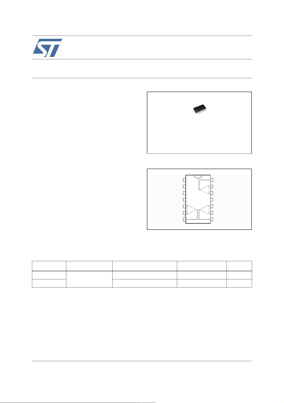
TSH93
D
SO-14
(Plastic Micropackage)
Pin Connections (top view)
N.C.
N.C.
N.C.
V
CC
Non-inverting Input 1
Inverting Input 1
Output 1
1
2
3
+
4
5
+
-
6
7
14
13
-
+
12
11
10
+
9
8
Output 3
Inverting Input 3
Non-inverting Input 3
-
V
CC
Non-inverting Input 2
Inverting Input 2
Output 2
High slew rate and low noise make it also suitable
for high quality audio applications.
Order Codes
Part Number Temperature Range Package Packaging Marking
TSH93ID/IDT
TSH93IYD/IYD SO-14 (automotive grade level) Tube or Tape & Reel H93Y
August 2005 1/12
SO-14 Tube or Tape & Reel H93
-40°C, +125°C
Rev 2
www.st.com
12
Page 2
Absolute Maximum Ratings TSH93
1 Absolute Maximum Ratings
Table 1. Key parameters and their absolute maximum ratings
Symbol Parameter Value Unit
(3)
(1)
(2)
CC
+
+0.3V.
14 V
±5 V
-0.3 to 12 V
V
CC Supply Voltage
V
Differential Input Voltage
id
V
Input Voltage
i
T
T
1. All voltages values, except differential voltage are with respect to network ground terminal.
2. Differential voltages are the non-inverting input terminal with respect to the inverting input terminal.
3. The magnitude of input and output voltages must never exceed V
Operating Free-Air Temperature range -40 to +125 °C
oper
Storage Temperature Range -65 to +150 °C
stg
Table 2. Operating conditions
Symbol Parameter Value Unit
V
Supply Voltage 7 to 12 V
CC
V
Common Mode Input Voltage Range
ic
V
CC
-
+2 to V
CC
+
-1
V
2/12
Page 3
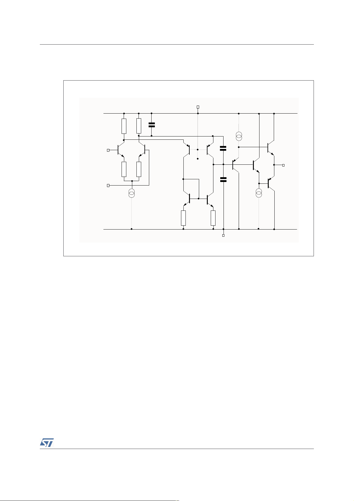
TSH93 Schematic Diagram
2 Schematic Diagram
Figure 1. Schematic diagram (1/3)
+
V
CC
non inverting
input
inverting
input
Internal
V
ref
output
C
c
-
V
CC
3/12
Page 4
Electrical Characteristics TSH93
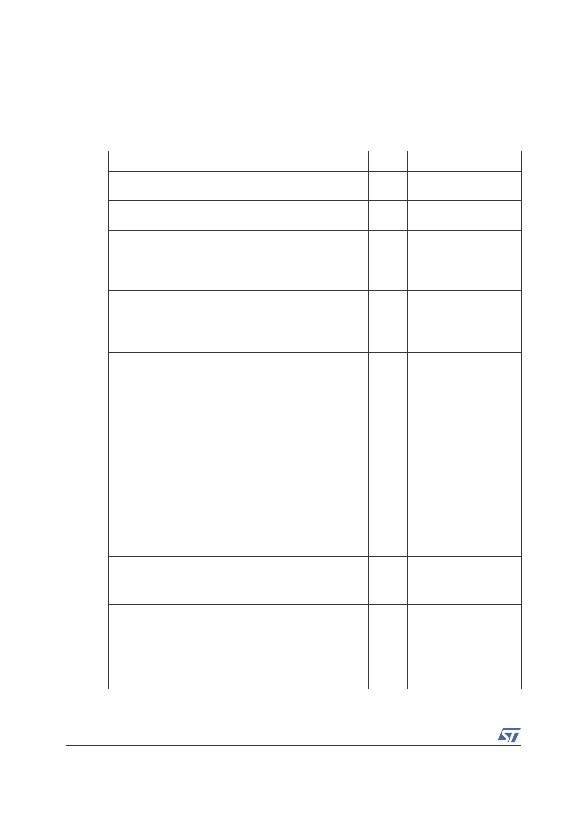
3 Electrical Characteristics
Table 3. V
CC
+
= 5V, V
-
= -5V, T
CC
= 25°C (unless otherwise specified)
amb
Symbol Parameter Min. Typ. Max. Unit
V
io
I
io
I
ib
I
CC
CMR
SVR
Avd
Input Offset Voltage
T
min
. ≤ T
amb
≤ T
max.
Input Offset Current
T
. ≤ T
min
Input Bias Current
T
. ≤ T
min
amb
amb
≤ T
≤ T
max.
.
max.
Supply Current (per amplifier, no load)
T
. ≤ T
min
Common-mode Rejection Ratio V
T
. ≤ T
min
Supply Voltage Rejection Ratio V
T
. ≤ T
min
Large Signal Voltage Gain R
T
. ≤ T
min
amb
amb
amb
amb
≤ T
≤ T
≤ T
≤ T
max.
max.
max
max.
= -3V to +4V, Vo = 0V
ic
= ±5V to ±3V
CC
= 100Ω, Vo = ±2.5V
L
80
70
60
50
57
54
12
515
4.5 6
100
75
70
4
6
5
20
8
High Level Output Voltage Vid = 1V
R
= 600Ω
V
OH
L
R
= 150Ω
L
T
min
. ≤ T
amb
≤ T
- RL = 150Ω
max.
3
2.5
2.4
3.5
3
Low Level Output Voltage Vid = 11V
R
= 600Ω
V
OL
L
R
= 150Ω
L
T
min
. ≤ T
amb
≤ T
max. - RL
= 150Ω
-3.5
-2.8
-3
-2.5
-2.4
Output Short Circuit Current - Vid = ±1V
Source
I
Sink
o
T
min
. ≤ T
amb
≤ T
max.
- Source
Sink
20
20
15
15
36
40 mA
mV
µA
µA
mA
dB
dB
dB
V
V
GBP
SR
φm
V
O1/VO2
Gain Bandwidth Product
A
= 100, RL = 600Ω, CL = 15pF, f = 7.5MHz
VCL
f
Transition Frequency 90 MHz
T
Slew Rate
V
= -2 to +2V, A
in
Equivalent Input Voltage Noise Rs = 50Ω, f = 1kHz
e
n
Phase Margin A
= +1, RL = 600Ω, CL = 15pF
VCL
= +1
VM
Channel Separation f = 1MHz to 10MHz 65 dB
4/12
90 150
62 110
4.2 nV/√Hz
35 Degrees
MHz
V/µs
Page 5

TSH93 Electrical Characteristics
Table 3. V
CC
+
= 5V, V
-
= -5V, T
CC
= 25°C (unless otherwise specified)
amb
Symbol Parameter Min. Typ. Max. Unit
Gain Flatness f = DC to 6MHz, A
Gf
THD
∆G
∆ϕ
Total Harmonic Distortion
f = 1kHz, V
Differential Gain f = 3.58MHz, A
Differential Phase f = 3.58MHz, A
Table 4. V
+
= ±15V, T
cc
= ±2.5V, RL = 600Ω
o
= 25°C (unless otherwise specified)
amb
= 10dB
VCL
= +2, RL = 150Ω
VCL
= +2, RL = 150Ω
VCL
0.1 dB
0.01 %
0.03 %
0.07 Degrees
Symbol Conditions Value Unit
V
A
I
CC
V
icm
V
OH
V
OL
I
sink
I
source
GBP
SR
φm
io
vd
RL = 600Ω
No load / Ampli 5.2 mA
RL = 600Ω
RL = 600Ω
Vo = 0V
Vo = 0V
= 600Ω, CL = 15pF
R
L
R
= 600Ω, CL = 15pF
L
= 600Ω, CL = 15pF
R
L
0mV
3.2 V/mV
-3 to 4 V
+3.6 V
-3.6 V
40 mA
40 mA
147 MHz
110 V/µs
42 Degrees
5/12
Page 6

Printed Circuit Layout TSH93
4 Printed Circuit Layout
As for any high frequency device, a few rules must be observed when designing the PCB to get
the best performances from this high speed op-amp.
From the most to the least important points:
● Each power supply lead has to be bypassed to ground with a 10nF ceramic capacitor very
close to the device and a 10µF capacitor.
● To provide low inductance and low resistance common return, use a ground plane or
common point return for power and signal.
● All leads must be wide and as short as possible especially for op-amp inputs. This is in
order to decrease parasitic capacitance and inductance.
● Use small resistor values to decrease time constant with parasitic capacitance.
● Choose component sizes as small as possible (SMD).
On output, decrease capacitor load so as to avoid circuit stability being degraded which may
cause oscillation. You can also add a serial resistor in order to minimize its influence.
6/12
Page 7

TSH93 Printed Circuit Layout
Figure 2. Input offset voltage drift vs.
temperature
Figure 4. Large signal follower response Figure 5. Small signal follower response
Figure 3. Static open loop voltage gain
Figure 6. Open loop frequency response &
phase shift
Figure 7. Close loop frequency response
7/12
Page 8

Printed Circuit Layout TSH93
Figure 8. Audio bandwidth frequency -
Response & phase shift (TSH93 vs.
standard 15MHz audio op-amp)
Figure 10. Cross talk isolation vs. frequency
(SO-14 package)
Figure 9. Gain flatness & phase shift vs.
frequency
Figure 11. Cross talk isolation vs. frequency
(SO-14 package)
Figure 12. Differential input impedance vs.
frequency
4.5
4.0
3.5
3.0
)
W
2.5
2.0
Zin-diff (k
1.5
1.0
0.5
1k 10k 100k 1M 10M 100M
8/12
Frequency (Hz)
Figure 13. Common input impedance vs.
frequency
120
100
80
)
W
60
Zin-com (M
40
20
1k 10k 100k 1M 10M 100M
Frequency (Hz)
Page 9

TSH93 Macromodels
5 Macromodels
Note: Note: Please consider following remarks before using this macromodel:
All models are a trade-off between accuracy and complexity (i.e. simulation time).
Macromodels are not a substitute to breadboarding; rather, they confirm the validity of a design
approach and help to select surrounding component values.
A macromodel emulates the NOMINAL performance of a TYPICAL device within SPECIFIED
OPERATING CONDITIONS (i.e. temperature, supply voltage, etc.). Thus the macromodel is
often not as exhaustive as the datasheet, its goal is to illustrate the main parameters of the
product.
Data issued from macromodels used outside of its specified conditions (Vcc, Temperature, etc.)
or even worse: outside of the device operating conditions (Vcc, Vicm, etc.) are not reliable in
any way.
Applies to: TSH93I
** Standard Linear Ics Macromodels, 1997.
** CONNECTIONS :
* 1 INVERTING INPUT
* 2 NON-INVERTING INPUT
* 3 OUTPUT
* 4 POSITIVEPOWER SUPPLY
* 5 NEGATIVE POWER SUPPLY
.SUBCKT TSH93 1 3 2 4 5(analog)
********************************************************
.MODEL MDTH D IS=1E-8 KF=1.809064E-15 CJO=10F
* INPUT STAGE
CIP 2 5 1.000000E-12
CIN 1 5 1.000000E-12
EIP 10 5 2 5 1
EIN 16 5 1 5 1
RIP 10 11 2.600000E-01
RIN 15 16 2.600000E-01
RIS 11 15 3.645298E-01
DIP 11 12 MDTH 400E-12
DIN 15 14 MDTH 400E-12
VOFP 12 13 DC 0.000000E+00
VOFN 13 14 DC 0
IPOL 13 5 1.000000E-03
CPS 11 15 2.986990E-10
DINN 17 13 MDTH 400E-12
VIN 17 5 2.000000e+00
DINR 15 18 MDTH 400E-12
VIP 4 18 1.000000E+00
FCP 4 5 VOFP 3.500000E+00
FCN 5 4 VOFN 3.500000E+00
FIBP 2 5 VOFP 1.000000E-02
FIBN 5 1 VOFN 1.000000E-02
* AMPLIFYING STAGE
FIP 5 19 VOFP 2.530000E+02
9/12
Page 10

Macromodels TSH93
FIN 5 19 VOFN 2.530000E+02
RG1 19 5 3.160721E+03
RG2 19 4 3.160721E+03
CC 19 5 2.00000E-09
DOPM 19 22 MDTH 400E-12
DONM 21 19 MDTH 400E-12
HOPM 22 28 VOUT 1.504000E+03
VIPM 28 4 5.000000E+01
HONM 21 27 VOUT 1.400000E+03
VINM 5 27 5.000000E+01
***********************
RZP1 5 80 1E+06
RZP2 4 80 1E+06
GZP 5 82 19 80 2.5E-05
RZP2H 83 4 10000
RZP1H 83 82 80000
RZP2B 84 5 10000
RZP1B 82 84 80000
LZPH 4 83 3.535e-02
LZPB 84 5 3.535e-02
EOUT 26 23 82 5 1
VOUT 23 5 0
ROUT 26 3 35
COUT 3 5 30.000000E-12
DOP 19 25 MDTH 400E-12
VOP 4 25 2.361965E+00
DON 24 19 MDTH 400E-12
VON 24 5 2.361965E+00
.ENDS
10/12
Page 11

TSH93 Package Mechanical Data
6 Package Mechanical Data
In order to meet environmental requirements, ST offers these devices in ECOPACK® packages.
These packages have a Lead-free second level interconnect. The category of second level
interconnect is marked on the package and on the inner box label, in compliance with JEDEC
Standard JESD97. The maximum ratings related to soldering conditions are also marked on
the inner box label. ECOPACK is an ST trademark. ECOPACK specifications are available at:
www.st.com
6.1 SO-14 Package
.
SO-14 MECHANICAL DATA
DIM.
A 1.75 0.068
a1 0.1 0.2 0.003 0.007
a2 1.65 0.064
b 0.35 0.46 0.013 0.018
b1 0.19 0.25 0.007 0.010
C 0.5 0.019
c1 45˚ (typ.)
D 8.55 8.75 0.336 0.344
E 5.8 6.2 0.228 0.244
e 1.27 0.050
e3 7.62 0.300
F 3.8 4.0 0.149 0.157
G 4.6 5.3 0.181 0.208
L 0.5 1.27 0.019 0.050
M 0.68 0.026
S˚ (max.)
MIN. TYP MAX. MIN. TYP. MAX.
mm. inch
8
PO13G
11/12
Page 12
Revision History TSH93
7 Revision History
Date Revision Changes
Oct. 2000 1 First Release
Aug. 2005 3
1 - PPAP references inserted in the datasheet see
on page 1
.
Table : Order Codes
Information furnished is believed to be accurate and reliable. However, STMicroelectronics assumes no responsibility for the consequences
of use of such information nor for any infringement of patents or other rights of third parties which may result from its use. No license is
granted by implication or otherwise under any patent or patent rights of STMicroelectronics. Specifications mentioned in this publication are
subject to change withou t notice. This publication supersedes and replaces all information previously supplied. STMicroelectronics products
are not authorized for use as critical components in life support devices or systems without express written approval of STMicroelectronics.
The ST logo is a registered trademark of STMicroelectronics.
All other names are the property of their respective owners
© 2005 STMicroelectronics - All rights reserved
STMicroelectronics group of companies
Australia - Belgium - Brazil - Canada - China - Czech Republic - Finland - France - Germany - Hong Kong - India - Israel - Italy - Japan -
Malaysia - Malta - Morocco - Singapore - Spain - Sweden - Switzerland - United Kingdom - United States of America
www.st.com
12/12
 Loading...