

Wide Band, Rail-to-Rail Operational Amplifier
■ 4.5V, 12V operating conditions
■ 3dB-bandwidth: 100MHz
■ Slew-rate: 100V/µs
■ Output current: up to 55mA
■ Input single supply voltage
■ Output rail-to-rail
■ Specified for 150Ω load
■ Low distortion, THD: 0.1%
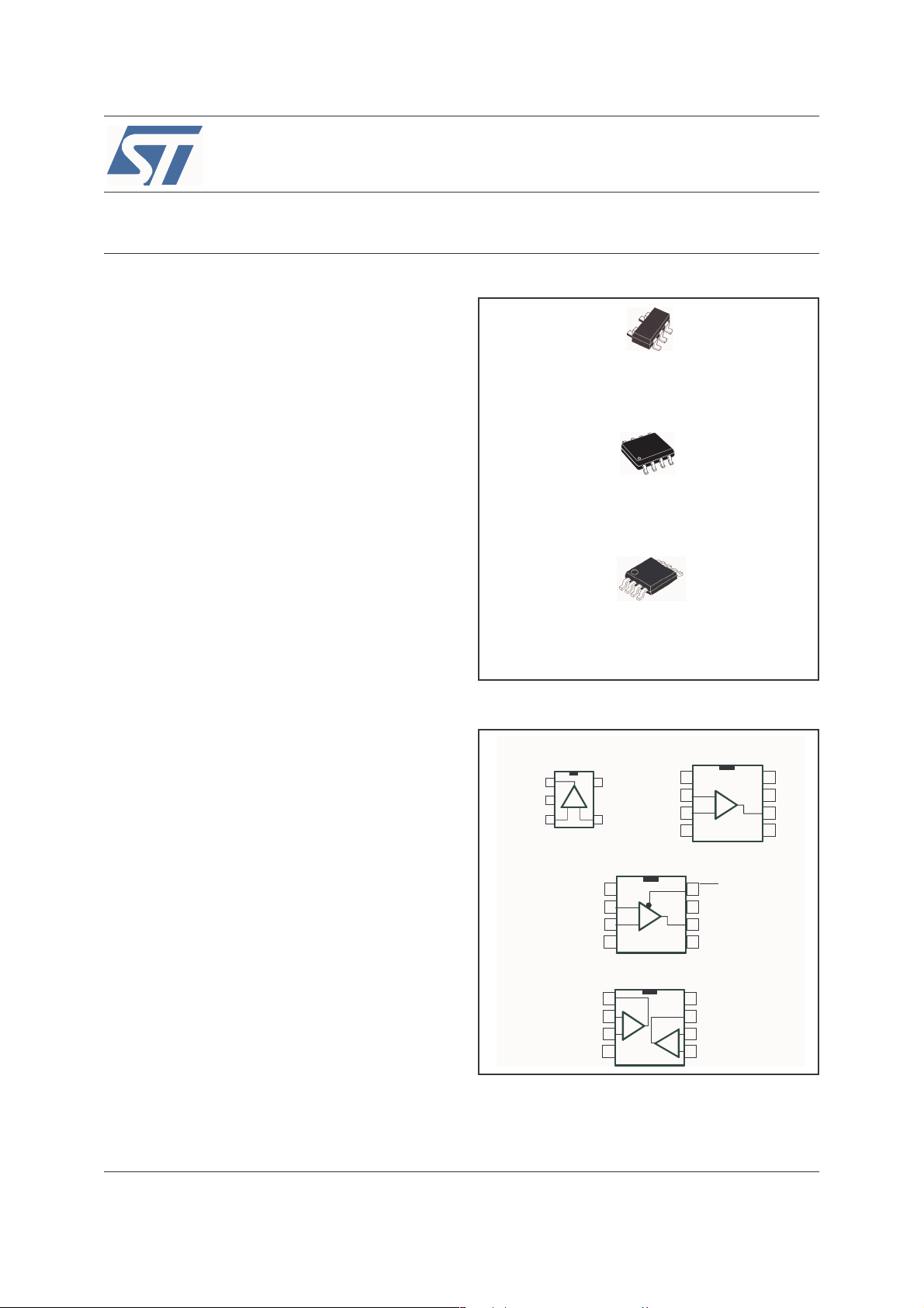
■ SOT23-5, TSSOP and SO packages
Description
The TSH8x series offers single and dual
operational amplifiers featuring high video
performances with large bandwidth, low distortion
and excellent supply voltage rejection. These
amplifiers feature also large output voltage swing
and high output current capability to drive
standard 150Ω loads.
TSH80-TSH81-TSH82
with Standby Function
L
SOT23-5
(Plastic Micro package)
D
SO-8
(Plastic Micro package)
P
TSSOP8
(Plastic Micro package)
Running at single or dual supply voltage from
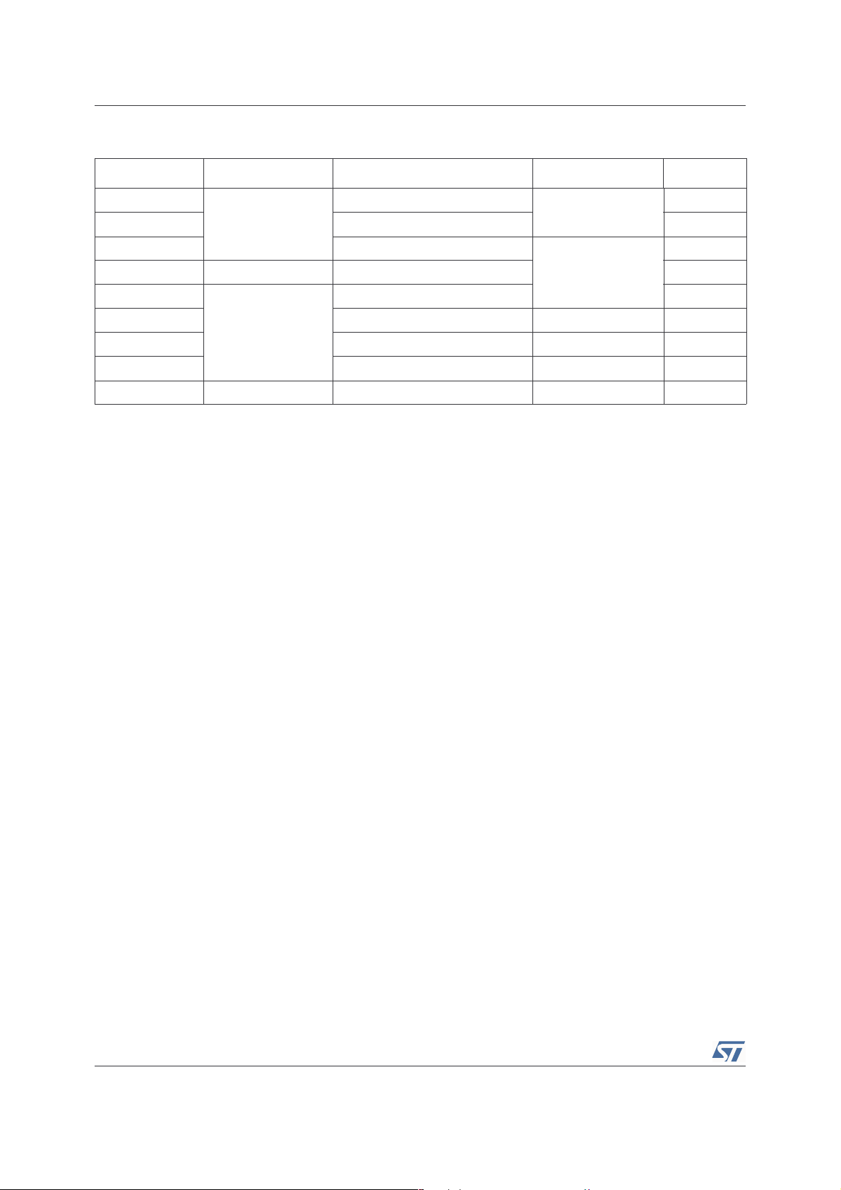
Pin Connections (top view)
4.5V to 12V, these amplifiers are tested at
5V(±2.5V) and 10V(±5V) supplies.
Output
The TSH81 also features a standby mode, which
allows the operational amplifier to be put into a
standby mode with low power consumption and
Output
VCC -
VCC -
Non-Inv. In.
Non-Inv. In.
high output impedance.The function allows power
saving or signals switching/multiplexing for high
speed applications and video applications.
For board space and weight saving, TSH8x series
is proposed in SOT23-5, TSSOP8 and SO-8
Non Inverting Input
Non Inverting Input
packages.
Application
■ Video buffers
■ A/D converters driver
■ Hi-Fi applications
August 2005 1/23
Non Inve rting Input1
Non Inve rting Input1
TSH80 : SOT23-5/SO8
TSH80 : SOT23-5/SO8
NC
NC
1
1
1
2
2
3
3
Inverting Input
Inverting Input
Inverting Input1 Output2
Inverting Input1 Output2
5
5
VCC +
VCC +
+ -
+ -
TSH81 : SO8/TSSOP8
TSH81 : SO8/TSSOP8
VCC -
VCC -
TSH82 : SO8/TSSOP8
TSH82 : SO8/TSSOP8
Output1
Output1
VCC -
VCC -
Non-Inv. I n.
Non-Inv. I n.
Inv. In.
Inv. In.
4
4
NC
NC
1
1
2
2
3
3
1
1
2
2
_
_
+
+
3
3
1
2
2
Inv. In.
Inv. In.
3
3
VCC -
VCC -
8
8
STANDBY
STANDBY
_
_
+
+
7
7
VCC +
VCC +
Output
Output
6
6
NC
NC
54
54
VCC +
VCC +
8
8
7
7
Inverting Input2
Inverting Input2
_
_
6
6
+
+
Non Inv erting I nput2
Non Inv erting I nput2
54
54
_
_
+
+
NC
NC
8
8
7
7
VCC +
VCC +
Output
Output
6
6
NC
NC
54
54
Rev 2
www.st.com
23
TSH80-TSH81-TSH82
Order Codes
Type Temperature Range Package Packaging Marking
TSH80ILT
TSH80IYLT SOT23-5 (automotive grade level) K310
TSH80ID/DT SO-8
TSH80IYD/IYDT -40°C to +125°C SO-8 (automotive grade level) SH80IY
TSH81ID/DT
TSH81IPT TSSOP8 Tape & Reel SH81I
TSH82ID/DT SO-8 Tube or Tape & Reel TSH82I
TSH82IPT TSSOP8 Tape & Reel SH82I
TSH82IYD/ITDT -40°C to +125°C SO-8 (automotive grade level) Tube or Tape & Reel SH82IY
-40°C to +85°C
-40°C to +85°C
SOT23-5
Tape & Reel
Tube or Tape & Reel
SO-8 TSH81I
K303
TSH80I
2/23
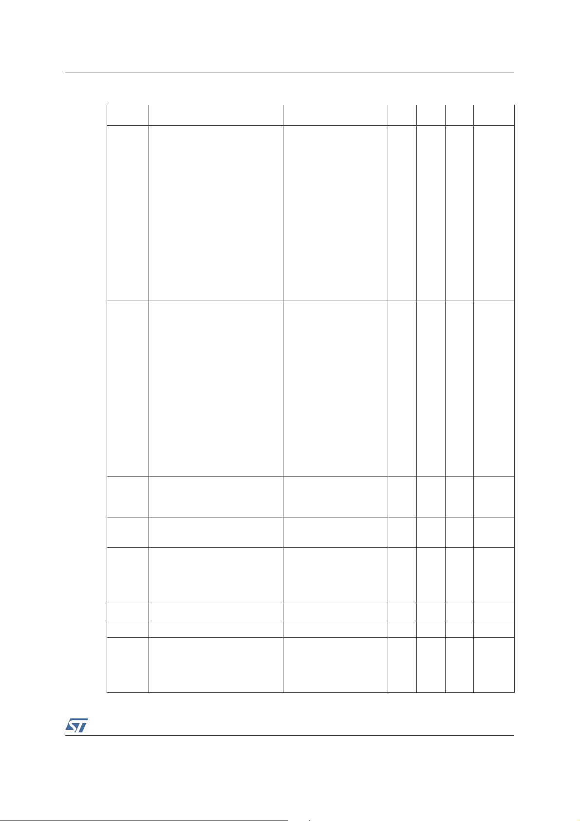
TSH80-TSH81-TSH82 Absolute Maximum Ratings
1 Absolute Maximum Ratings
Table 1. Key parameters and their absolute maximum ratings
Symbol Parameter Value Unit
(3)
(1)
(2)
14 V
±2V
±6V
(4)
80
28
37
V
CC Supply Voltage
T
V
T
id
V
oper
stg
T
Differential Input Voltage
Input Voltage
i
Operating Free Air Temperature Range -40 to +85 °C
Storage Temperature -65 to +150 °C
Maximum Junction Temperature 150 °C
j
Thermal resistance junction to case
R
thjc
SOT23-5
SO8
TSSOPO8
Thermal resistance junction to ambient area
R
thja
SOT23-5
SO8
TSSOPO8
250
157
130
ESD Human Body Model 2 kV
1. All voltage values, except differential voltage are with respect to network ground terminal
2. Differential voltages are non-inverting input terminal with respect to the inverting terminal
3. The magnitude of input and output must never exceed VCC +0.3V
4. Short-circuits can cause excessive heating
°C/W
°C/W
Table 2. Operating conditions
Symbol Parameter Value Unit
V
V
Standby
Supply Voltage 4.5 to 12 V
CC
Common Mode Input Voltage Range
IC
-
V
to (V
CC
-
) to (V
(V
CC
CC
+
-1.1)
CC
+
)
V
V
3/23
Electrical Characteristics TSH80-TSH81-TSH82
2 Electrical Characteristics
Table 3. V
CC
+
= +5V, V
-
= GND, Vic = 2.5V, T
CC
= 25°C (unless otherwise specified)
amb
Symbol Parameter Test Condition Min. Typ. Max. Unit
|V
∆V
C
I
T
|
Input Offset Voltage
io
Input Offset Voltage Drift vs.
io
Temperature
I
Input Offset Current
io
I
Input Bias Current
ib
Input Capacitance 0.3 pF
in
Supply Current per Operator
CC
T
T
T
T
T
T
T
T
amb
min.
min.
amb
min.
amb
min.
amb
min.
< T
amb
< T
amb
= 25°C
< T
amb
= 25°C
< T
amb
= 25°C
< T
amb
< T
< T
< T
< T
< T
max.
max.
max.
max.
max.
1.1 10
12
3 µV/°C
0.1 3.5
5
615
20
8.2 10.5
11.5
= 25°C
+0.1<Vic<3.9V &
CMR
SVR
PSR
Common Mode Rejection Ratio
(δVic/δVio)
Supply Voltage Rejection Ratio
(δVcc/δVio)
Power Supply Rejection Ratio
(δVcc/δVou t )
Vout=2.5V
T
= 25°C
amb
T
< T
min.
= 25°C
T
amb
T
< T
min.
amb
amb
< T
< T
max.
max.
727097 dB
686575
Positive & Negative Rail 75 dB
mV
µA
µA
mA
dB
A
Large Signal Voltage Gain
vd
Output Short Circuit Current
I
o
Source
4/23
=150Ω to 1.5V
R
L
V
=1V to 4V
out
T
= 25°C
amb
T
< T
min.
amb
=25°C
T
amb
V
=+1, V
id
V
id
=-1, V
out
out
|Source|
Sink
T
< T
min.
amb
Vid=+1, V
V
id
=-1, V
out
out
|Source|
Sink
< T
max.
to 1.5V
to 1.5V
< T
max.
to 1.5V
to 1.5V
757084
55
35
55
33
28
28
dB
mA
TSH80-TSH81-TSH82 Electrical Characteristics
Table 3. V
CC
+
= +5V, V
-
= GND, Vic = 2.5V, T
CC
= 25°C (unless otherwise specified)
amb
Symbol Parameter Test Condition Min. Typ. Max. Unit
T
=25°C
amb
R
= 150Ω to GND
L
R
= 600Ω to GND
L
R
= 2kΩ to GND
L
R
= 10kΩ to GND
L
R
= 150Ω to 2.5V
V
High Level Output Voltage
oh
L
R
= 600Ω to 2.5V
L
R
= 2kΩ to 2.5V
L
R
= 10kΩ to 2.5V
L
< T
T
min.
amb
< T
max.
RL = 150Ω to GND
R
= 150Ω to 2.5V
L
T
=25°C
amb
R
= 150Ω to GND
L
R
= 600Ω to GND
L
R
= 2kΩ to GND
L
R
= 10kΩ to GND
L
4.2
4.5
4.1
4.4
4.36
4.85
4.90
4.93
4.66
4.90
4.92
4.93
48
54
55
56
150
V
400
= 150Ω to 2.5V
R
V
Low Level Output Voltage
ol
L
R
= 600Ω to 2.5V
L
R
= 2kΩ to 2.5V
L
R
= 10kΩ to 2.5V
L
< T
T
min.
amb
< T
max.
RL = 150Ω to GND
R
= 150Ω to 2.5V
L
220
105
76
61
mV
200
450
F=10MHz
A
GBP Gain Bandwidth Product
Bw Bandwidth @-3dB
SR Slew Rate
φm Phase Margin
=+11
VCL
A
=-10
VCL
A
=+1
VCL
R
=150Ω to 2.5V
L
=+2
A
VCL
R
=150Ω // CL to 2.5V
L
C
= 5pF
L
C
= 30pF
L
R
=150Ω // 30pF to 2.5V
L
65
55
87 MHz
104
60
105
40 °
MHz
V/µs
en Equivalent Input Noise Voltage F=100kHz 11 nV/√Hz
A
=+2, F=4MHz
VCL
R
=150Ω // 30pF to 2.5V
THD Total Harmonic Distortion
V
V
L
out
out
=1Vpp
=2Vpp
-61
-54
dB
5/23
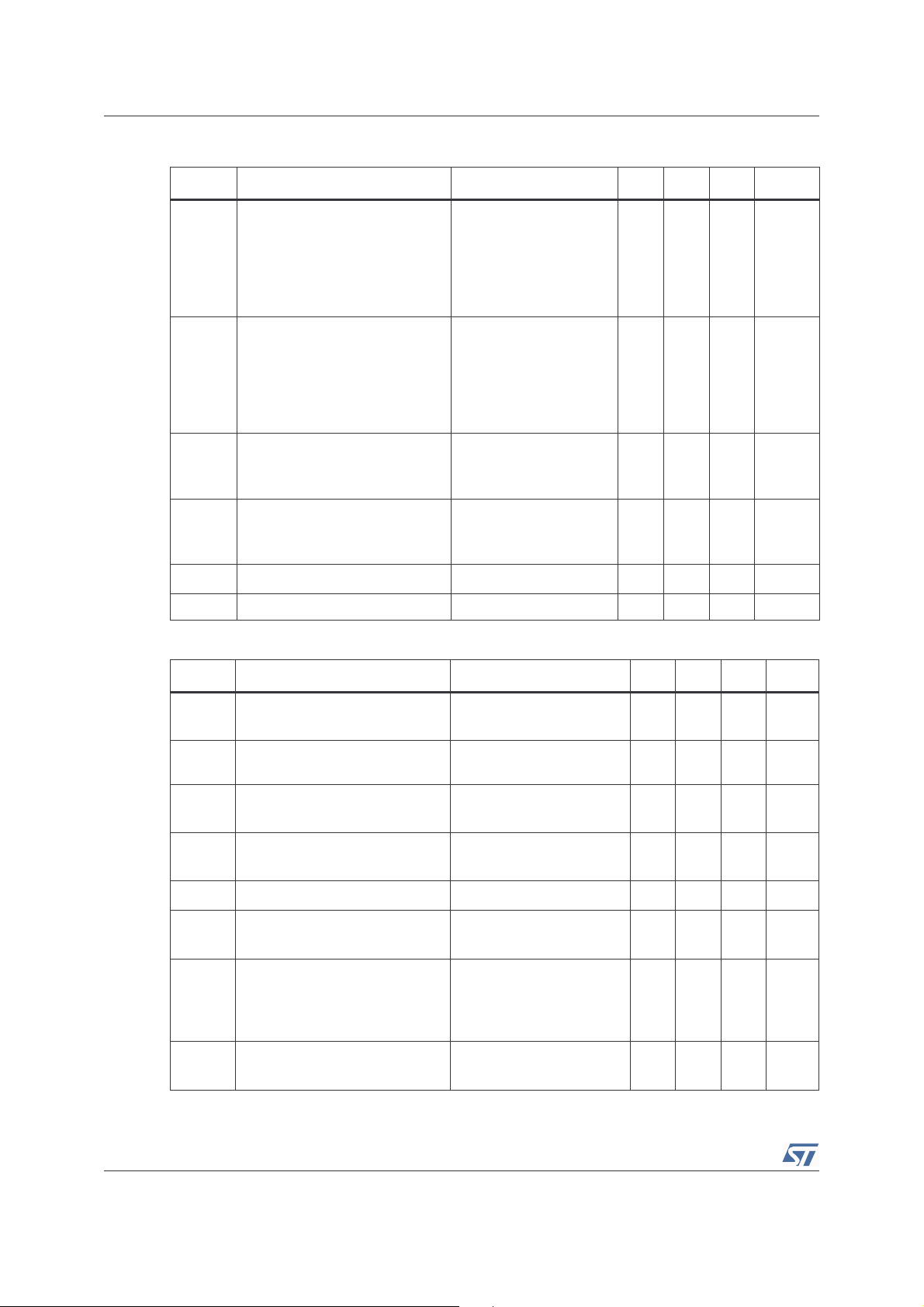
Electrical Characteristics TSH80-TSH81-TSH82
Table 3. V
CC
+
= +5V, V
-
= GND, Vic = 2.5V, T
CC
= 25°C (unless otherwise specified)
amb
Symbol Parameter Test Condition Min. Typ. Max. Unit
A
IM2
Second order inter modulation
product
=+2, V
VCL
R
=150Ω to 2.5V
L
Fin1=180kHz,
Fin2=280kHz
out
=2Vpp
-76 dBc
spurious measurement
@100kHz
A
IM3
Third order inter modulation
product
=+2, V
VCL
R
=150Ω to 2.5V
L
Fin1=180kHz,
Fin2=280KHz
out
=2Vpp
-68 dBc
spurious measurement
@400kHz
A
=+2, RL=150Ω to
VCL
∆G Differential gain
Df Differential phase
Gf Gain Flatness
2.5V
F=4.5MHz, V
=+2, RL=150Ω to
A
VCL
out
2.5V
F=4.5MHz, V
out
F=DC to 6MHz, A
=2Vpp
=2Vpp
VCL
=+2
0.5 %
0.5 °
0.2 dB
Vo1/Vo2 Channel Separation F=1MHz to 10MHz 65 dB
Table 4. V
CC
+
= +5V, V
-
= -5V, Vic = GND, T
CC
= 25°C (unless otherwise specified)
amb
Symbol Parameter Test Condition Min. Typ. Max. Unit
|V
∆V
C
I
T
|
Input Offset Voltage
io
Input Offset Voltage Drift vs.
io
Temperature
I
Input Offset Current
io
I
Input Bias Current
ib
Input Capacitance 0.7 pF
in
Supply Current per Operator
CC
T
T
T
T
T
T
T
T
amb
min.
min.
amb
min.
amb
min.
amb
min.
< T
amb
< T
amb
= 25°C
< T
amb
= 25°C
< T
amb
= 25°C
< T
amb
< T
< T
< T
< T
< T
max.
max.
max.
max.
max.
0.8 10
12
2 µV/°C
0.1 3.5
5
615
20
9.8 12.3
13.4
= 25°C
-4.9 < Vic < 3.9V &
CMR
SVR
Common Mode Rejection Ratio
(δVic/δVio)
Supply Voltage Rejection Ratio
(δVCC/δVio)
Vout=GND
T
= 25°C
amb
T
< T
min.
= 25°C
T
amb
T
< T
min.
amb
amb
< T
< T
8172106 dB
max.
716577
max.
mV
µA
µA
mA
dB
6/23
TSH80-TSH81-TSH82 Electrical Characteristics
Table 4. V
CC
+
= +5V, V
-
= -5V, Vic = GND, T
CC
= 25°C (unless otherwise specified)
amb
Symbol Parameter Test Condition Min. Typ. Max. Unit
PSR
A
V
Power Supply Rejection Ratio
(δVCC/δVout )
Large Signal Voltage Gain
vd
Output Short Circuit Current
I
o
Source
High Level Output Voltage
oh
Positive & Negative Rail 75 dB
=150Ω to GND
R
L
V
=-4 to +4
out
T
= 25°C
amb
T
< T
min.
amb
T
=25°C
amb
V
=+1, V
id
V
id
=-1, V
out
out
|Source|
Sink
T
< T
min.
amb
Vid=+1, V
V
id
=-1, V
out
out
|Source|
Sink
T
=25°C
amb
R
= 150Ω to GND
L
R
= 600Ω to GND
L
R
= 2kΩ to GND
L
R
= 10kΩ to GND
L
< T
max.
to 1.5V
to 1.5V
< T
max.
to 1.5V
to 1.5V
757086
35
30
28
28
4.2
4.36
4.85
4.9
4.93
55
55
dB
mA
V
V
Low Level Output Voltage
ol
GBP Gain Bandwidth Product
Bw Bandwidth @-3dB
SR Slew Rate
φmPhase Margin
T
< T
amb
< T
max.
min.
RL = 150Ω to GND
T
=25°C
amb
R
= 150Ω to GND
L
R
= 600Ω to GND
L
R
= 2kΩ to GND
L
R
= 10kΩ to GND
L
T
< T
amb
< T
max.
min.
RL = 150Ω to GND
F=10MHz
A
=+11
VCL
=-10
A
VCL
=+1
A
VCL
R
=150Ω // 30pF to GND
L
=+2
A
VCL
R
=150Ω // CL to GND
L
C
= 5pF
L
C
= 30pF
L
R
=150Ω to gnd
L
4.1
-4.63
-4.86
-4.9
-4.93
65
55
100 MHz
117
68
118
40 °
-4.4
mV
-4.3
MHz
V/µs
7/23

Electrical Characteristics TSH80-TSH81-TSH82
Table 4. V
CC
+
= +5V, V
-
= -5V, Vic = GND, T
CC
= 25°C (unless otherwise specified)
amb
Symbol Parameter Test Condition Min. Typ. Max. Unit
en Equivalent Input Noise Voltage F=100kHz 11
A
=+2, F=4MHz
VCL
R
=150Ω // 30pF to gnd
THD Total Harmonic Distortion
IM2
Second order inter modulation
product
L
V
=1Vpp
out
V
=2Vpp
out
A
=+2, V
VCL
R
=150Ω to gnd
L
out
Fin1=180kHz,
Fin2=280KHz
-61
-54
=2Vpp
-76 dBc
spurious measurement
@100kHz
A
IM3
Third order inter modulation
product
=+2, V
VCL
R
=150Ω to gnd
L
Fin1=180kHz,
Fin2=280KHz
out
=2Vpp
-68 dBc
spurious measurement
@400kHz
A
=+2, RL=150Ω to gnd
∆G Differential gain
Df Differential phase
Gf Gain Flatness
VCL
F=4.5MHz, V
=+2, RL=150Ω to gnd
A
VCL
F=4.5MHz, V
out
out
F=DC to 6MHz, A
=2Vpp
=2Vpp
VCL
=+2
0.5 %
0.5 °
0.2 dB
Vo1/Vo2 Channel Separation F=1MHz to 10MHz 65 dB
nV/
√Hz
dB
8/23

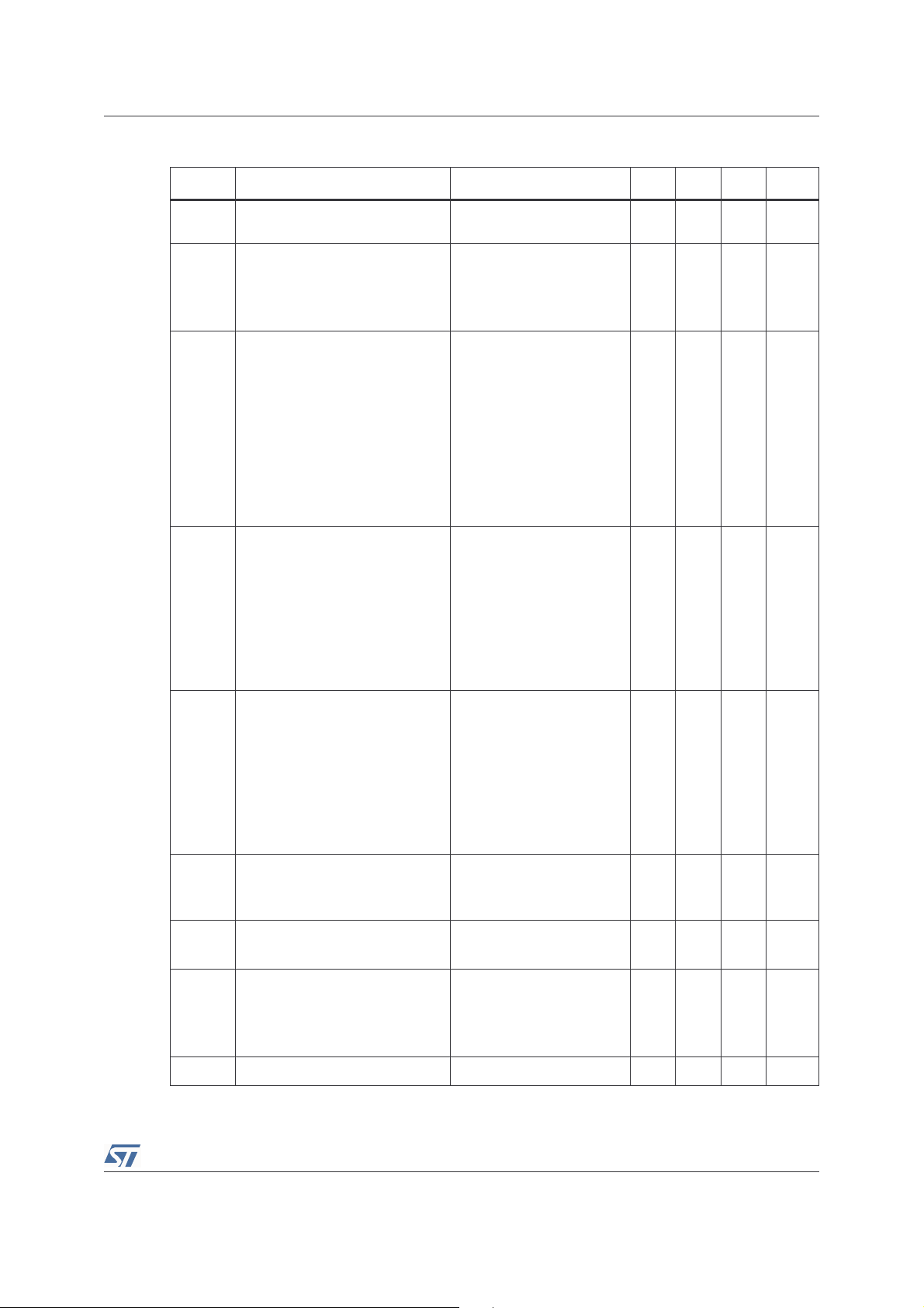
TSH80-TSH81-TSH82 Electrical Characteristics
Table 5. Standby mode
+
, V
CC
-
, T
= 25°C (unless otherwise specified)
amb
V
CC
Symbol Parameter Test Condition Min. Typ. Max. Unit
Vl
V
Standby Low Level
ow
Standby High Level
high
Current Consumption per
I
CC SBY
Operator when STANDBY is
Active
Z
T
T
Output Impedance (Rout//
out
Cout)
Time from Standby Mode to
on
Active Mode
Time from Active Mode to
off
Standby Mode
TSH81 STANDBY CONTROL pin 8 (SBY
V
low
V
high
-
V
CC
-
+2) (V
(V
CC
=
CC
-
pin 8 (TSH81) to V
R
out
C
out
Down to I
CC SBY
10µA
) OPERATOR STATUS
Standby
Active
(V
CC
-
+0.8)
+
CC
V
V
)
20 55 µA
10
17
MΩ
pF
2 µs
10 µs
9/23

Electrical Characteristics TSH80-TSH81-TSH82
Figure 1. Closed loop gain & phase vs.
frequency
Gain=+2, Vcc= ±2.5V, R
10
5
0
-5
Gain (dB)
-10
-15
1E+4 1E+5 1E+6 1E+7 1E+8 1E+9
Frequency (Hz)
=150Ω, T
L
Gain
Phase
= 25°C Gain=+2, Vcc= ±2.5V, T
amb
200
100
0
-100
-200
Figure 3. Closed loop gain & phase vs.
frequency
Gain=-10, Vcc= ±2.5V, R
30
20
Gain
10
Gain (dB)
0
=150Ω, T
L
Phase
= 25°C Gain=+11, Vcc= ±2.5V, RL=150Ω, T
amb
200
150
100
50
0
-50
Figure 2. Overshoot function of output
capacitance
= 25°C
amb
10
150Ω//33pF
5
150
Phase (°)
Gain (dB)
0
-5
1E+6 1E+7 1E+8 1E+9
Ω
Frequency (Hz)
150Ω//22pF
150Ω//10pF
Figure 4. Closed loop gain & phase vs.
frequency
= 25°C
amb
30
Phase
20
Gain
10
Phase (°)
Gain (dB)
0
0
-50
-100
Phase (°)
-10
1E+4 1E+5 1E+6 1E+7 1E+8 1E+9
-100
Frequency (Hz)
Figure 5. Large signal measurement - positive
slew rate
Gain=2,Vcc=±2.5V,Z
3
2
1
0
Vout (V)
-1
-2
-3
0 1020304050607080
10/23
L
=150Ω//5.6pF,Vin=400mVpk Gain=2,Vcc=±2.5V,ZL=150Ω//5.6pF,Vin=400mVpk
Time (ns)
-10
1E+4 1E+5 1E+6 1E+7 1E+8 1E+9
-150
Frequency (Hz)
Figure 6. Large signal measurement -
negative slew rate
3
2
1
0
Vout (V)
-1
-2
-3
0 1020304050 6070
Time (ns)

TSH80-TSH81-TSH82 Electrical Characteristics
Figure 7. Small signal measurement - rise time Figure 8. Small signal measurement - fall time
Gain=2,Vcc=±2.5V,Zl=150Ω,Vin=400mVpk Gain= 2,V cc=±2.5V,Zl=150Ω,Vin=400mVpk
0.06
0.04
0.02
0
Vin
Vin, Vout (V)
-0.02
-0.04
-0.06
0 102030405060
Vout
Time (ns)
Figure 9. Channel separation (Xtalk) vs.
frequency
Figure 10. Channel separation (Xtalk) vs.
0.06
0.04
0.02
0
Vin Vout (V)
-0.02
-0.04
-0.06
0 102030405060
Vin
Vout
Time (ns)
frequency
Measurement configuration: Xtalk=20log(V0/V1) Gain=+11, Vcc=±2.5V, ZL=150Ω//27pF
VIN
49.9
49.9
Ω
100
Ω
100
+
+
-
-
1kΩ
Ω
V1
150Ω
+
-
Ω
1k
Ω
150
VO
Ω
-20
-30
-40
-50
-60
-70
Xtalk (dB)
-80
-90
-100
-110
1E+4 1E+5 1E+6 1E+7
3/1output
4/1output
2/1output
Frequency (Hz)
Figure 11. Equivalent noise voltage Figure 12. Maximum output swing
Gain=100, Vcc=±2.5V, No load Gain=11, Vcc=±2.5V, RL=150Ω
30
+
25
20
Hz)
√
15
en (nV/
10
5
0.1 1 10 100 10 00
_
10k
100
Frequency (kHz)
3
2
1
0
Vin, Vout (V)
-1
-2
-3
0.0E+0 5.0E-2 1 .0E-1 1.5E-1 2.0E -1
Vout
Vin
Time (ms)
11/23

Inter Modulation Products TSH80-TSH81-TSH82
3 Inter Modulation Products
The IFR2026 synthesizer generates a two tones signal (F1=180kHz, F2=280kHz); each tone
having the same amplitude level.
The HP3585 spectrum analyzer measures the inter modulation products function of the output
voltage. The generator and the spectrum analyzer are phase locked for precision
considerations.
Figure 13. Standby mode - Ton, Toff Figure 14. Group delay
Vcc= ±2.5V, Open Loop Gain=2, Vcc= ±2.5V, ZL=150Ω//27pF, T
amb
= 25°C
3
2
1
0
-1
Vin, Vout (V)
-2
-3
Ton Toff
0 2E-6 4E-6 6E- 6 8E-6 1E-5
Vout
Standby
Time (s)
Vin
Figure 15. Third order inter modulation
Gain=2, Vcc= ±2.5V, ZL=150Ω//27pF, T
0
-10
-20
-30
-40
80kHz
380kHz
740kHz
640kHz
Vout peak(V)
-50
-60
IM3 (dBc)
-70
-80
-90
-100
01234
amb
= 25°C
5.32ns
Gain
Group
Delay
12/23

TSH80-TSH81-TSH82 Inter Modulation Products
Figure 16. Closed loop gain & phase vs.
frequency
Gain=+2, Vcc= ±5V, R
10
5
0
-5
Gain ( dB)
-10
-15
1E+4 1E+5 1E+6 1E+7 1E+8 1 E+9
Frequency (Hz)
=150Ω, T
L
Gain
Phase
= 25°C Gain=+2, Vcc= ±5V, T
amb
200
100
0
-100
-200
Figure 18. Closed loop gain & phase vs.
frequency
Gain=-10, Vcc= ±5V, R
30
20
Gain
10
Gain (dB)
0
=150Ω, T
L
Phase
= 25°C Gain=+11, Vcc= ±5V, RL=150Ω, T
amb
200
150
100
50
0
Figure 17. Overshoot function of output
capacitance
= 25°C
amb
10
150Ω//33pF
5
150
Phase (°)
Gain (dB)
0
-5
1E+6 1E+7 1E+8 1E+9
Ω
Frequency (Hz)
150Ω//22pF
150Ω//10pF
Figure 19. Closed loop gain & phase vs.
frequency
= 25°C
amb
30
Phase
20
Gain
10
Phase (°)
Gain (dB)
0
0
-50
Phase (°)
-100
-10
1E+4 1E+5 1E+6
1E+7 1E+8
1E+9
-50
Frequency (Hz)
Figure 20. Large signal measurement - positive
slew rate
Gain=2,Vcc=±5V,Z
5
4
3
2
1
0
Vout (V)
-1
-2
-3
-4
-5
0 20406080100
L
=150Ω//5.6pF,Vin=400mVpk Gain=2,Vcc=±5V,ZL=150Ω//5.6pF,Vin=400mVpk
Time (ns)
-10
1E+4 1E+5 1E+6 1E+7 1E+8 1E+9
Frequency (Hz)
Figure 21. Large signal measurement -
negative slew rate
5
4
3
2
1
0
Vout (V)
-1
-2
-3
-4
-5
0 20406080100
Time (ns)
-150
13/23

Inter Modulation Products TSH80-TSH81-TSH82
Figure 22. Small signal measurement - rise
Figure 23. Small signal measurement - fall time
time
Gain=2,Vcc=±5V,Zl=150Ω,Vin=400mVpk Gain=2,Vcc=±5V,Zl=150Ω,Vin=400mVpk
0.06
0.04
0.02
0
Vin, Vout (V)
-0.02
-0.04
-0.06
0 102030405060
Vin
Vout
Time (ns)
Figure 24. Channel separation (Xtalk) vs.
frequency
Figure 25. Channel separation (Xtalk) vs.
0.06
0.04
0.02
0
Vin, Vout (V)
-0.02
-0.04
-0.06
0 102030405060
Vin
Vout
Time (ns)
frequency
Measurement configuration: Xtalk=20log(V0/V1) Gain=+11, Vcc=±5V, ZL=150Ω//27pF
VIN
49.9
49.9
Ω
100Ω
Ω
100Ω
+
+
-
-
1kΩ
150
V1
Ω
+
-
1k
Ω
150
VO
Ω
-20
-30
-40
-50
-60
-70
Xtalk (dB)
-80
-90
-100
-110
1E+4 1E+5 1E+6
Frequency (Hz)
3/1output
4/1output
2/1output
1E+7
Figure 26. Equivalent noise voltage Figure 27. Maximum output swing
Gain=100, Vcc=±5V, No load Gain=11, Vcc=±5V, RL=150Ω
30
25
20
15
+
_
10k
100
en (nV/√Hz)
10
5
0.1 1 10 100 1000
Frequenc y (kHz)
14/23
5
4
3
2
1
0
-1
Vin, Vout (V)
-2
-3
-4
-5
0.0E+0 5.0E-2 1.0E-1 1.5E-1 2.0E-1
Vout
Vin
Time (ms)

TSH80-TSH81-TSH82 Inter Modulation Products
The IFR2026 synthesizer generates a two tones signal (F1=180kHz, F2=280kHz); each tone
having the same amplitude level.
The HP3585 spectrum analyzer measures the inter modulation products function of the output
voltage. The generator and the spectrum analyzer are phase locked for precision
considerations.
Figure 28. Standby mode - Ton, Toff Figure 29. Group delay
Vcc= ±5V, Open Loop Gain=2, Vcc= ±5V, ZL=150Ω//27pF, T
amb
= 25°C
5
Vout
0
Vin
Vin, Vout (V)
-5
Ton Toff
0 2E-6 4E-6 6E-6 8E-6
Standby
Time (s)
Figure 30. Third order inter modulation
Gain=2, Vcc= ±5V, ZL=150Ω//27pF, T
0
-10
-20
-30
-40
-50
740kHz
-60
IM3 (dBc)
-70
-80
-90
-100
01234
640kHz
Vout peak(V)
amb
80kHz
380kHz
= 25°C
Gain
Group
Delay
5.1ns
15/23

Testing Conditions TSH80-TSH81-TSH82
4 Testing Conditions
4.1 Layout precautions:
To use the TSH8X circuits in the best manner at high frequencies, some precautions have to be
taken for power supplies:
● First of all, the implementation of a proper ground plane in both sides of the PCB is
mandatory for high speed circuit applications to provide low inductance and low resistance
common return.
● Power supply bypass capacitors (4.7uF and ceramic 100pF) should be placed as close as
possible to the IC pins in order to improve high frequency bypassing and reduce harmonic
distortion. The power supply capacitors must be incorporated for both the negative and the
positive pins.
● Proper termination of all inputs and outputs must be in accordance with output termination
resistors; then the amplifier load will be only resistive and the stability of the amplifier will
be improved.
All leads must be wide and as short as possible especially for op amp inputs and outputs
in order to decrease parasitic capacitance and inductance.
● For lower gain application, attention should be paid not to use large feedback resistance
(>1kΩ) to reduce time constant with parasitic capacitances.
● Choose component sizes as small as possible (SMD).
● Finally, on output, the load capacitance must be negligible to maintain good stability. You
can put a serial resistance the closest to the output pin to minimize its influence.
Figure 31. CCIR330 video line
4.2 Maximum input level:
The input level must not exceed the following values:
● Negative peak: must be greater than -Vcc+400mV.
● Positive peak value: must be lower than +Vcc-400mV.
The electrical characteristics show the influence of the load on this parameter.
16/23

TSH80-TSH81-TSH82 Testing Conditions
4.3 Video capabilities:
To characterize the differential phase and differential gain a CCIR330 video line is used.
The video line contains 5 (flat) levels of luma on which is superimposed chroma signal. (the first
level contains no luma). The luma gives various amplitudes which define the saturation of the
signal. The chrominance gives various phases which define the color of the signal.
Differential phase (respectively differential gain) distortion is present if a signal chrominance
phase (gain) is affected by luminance level. They represent the ability to uniformly process the
high frequency information at all luminance levels.
When differential gain is present, color saturation is not correctly reproduced.
The input generator is the Rhode & Schwarz CCVS. The output measurement is done by the
Rhode and Schwarz VSA.
Figure 32. Measurement on Rhode and Schwarz VSA
Table 6. Video results
Parameter Value (Vcc=±2.5V) Value (Vcc=±5V) Unit
Lum NL 0.1 0.3 %
Lum NL Step 1 100 100 %
Lum NL Step 2 100 99.9 %
Lum NL Step 3 99.9 99.8 %
Lum NL Step 4 99.9 99.9 %
Lum NL Step 5 99.9 99.7 %
Diff Gain pos 0 0 %
Diff Gain neg -0.7 -0.6 %
Diff Gain pp 0.7 0.6 %
Diff Gain Step1 -0.5 -0.3 %
Diff Gain Step2 -0.7 -0.6 %
Diff Gain Step3 -0.3 -0.5 %
Diff Gain Step4 -0.1 -0.3 %
Diff Gain Step5 -0.4 -0.5 %
Diff Phase pos 0 0.1 deg
Diff Phase neg -0.2 -0.4 deg
Diff Phase pp 0.2 0.5 deg
Diff Phase Step1 -0.2 -0.4 deg
Diff Phase Step2 -0.1 -0.4 deg
Diff Phase Step3 -0.1 -0.3 deg
Diff Phase Step4 0 0.1 deg
Diff Phase Step5 -0.2 -0.1 deg
17/23

Precautions on Asymmetrical Supply Operation TSH80-TSH81-TSH82
5 Precautions on Asymmetrical Supply Operation
The TSH8X can be used either with a dual or a single supply. If a single supply is used, the
inputs are biased to the mid-supply voltage (+Vcc/2). This bias network must be carefully
designed, in order to reject any noise present on the supply rail.
As the bias current is 15uA, you must carefully choose the resistance R1 not to introduce an
offset mismatch at the amplifier inputs.
Cin
IN
R2
R3
Vcc+
C1C3C2
R4
R1
R1=10kΩ will be convenient. C1, C2, C3 are bypass capacitors from perturbation on Vcc as
well as for the input and output signals. We choose C1=100nF and C2=C3=100uF.
Cout
+
-
R5
Cf
OUT
RL
R2, R3 are such that the current through them must be superior to 100 times the bias current.
So, we take R2=R3=4.7kΩ.
Cin, as Cout are chosen to filter the DC signal by the low pass filters (R1,Cin) and (Rout, Cout).
By taking R1=10kΩ, RL=150Ω, and Cin=2uF, Cout=220uF we provide a cutoff frequency below
10Hz.
Figure 33. Use of the TSH8x in gain = -1 configuration
Cf
1k
Cout
-
+
OUT
RL
IN
Cin
R1
R2
R3 C 1C3C2
1k
Vcc+
Some precautions have to be added, specially for low power supply application.
A feedback capacitance Cf should be added for better stability.
The table summarizes the impact of the capacitance Cf on the phase margin of the circuit.
18/23

TSH80-TSH81-TSH82 Precautions on Asymmetrical Supply Operation
Table 7. Capacitance Cf on the phase margin of the circuit
Parameter Cf (pF) Vcc=±1.5V Vcc=±2.5V Vcc=±5V Unit
Phase Margin
f-3dB 40 39.3 38.3 MHz
Phase Margin
f-3dB 40 39.3 38.3 MHz
Phase Margin
f-3dB 37 34 32 MHz
Phase Margin
f-3dB 33.7 30.7 27.6 MHz
0
5.6
22
33
28 43 56 deg
30 43 56 deg
37 52 67 deg
48 65 78 deg
Figure 34. Example of a video application
Re
Ce
Vcc/2
Vcc/2
Rb1
R1
AOP 1
+
-
R2
R3 C3
V1
Cf
R7 C7
PA L
V2 V3
A1
LPF1
NTSC
A2
LPF2
IN
R4
R8
C4
C8
Vcc/2
Vcc/2
Vcc/2
Vcc/2
Rb1
Rb1
R5
R9
+
-
+
-
AOP2
R6
Cf
Standby
AOP 3
R10
Cf
Standby
V4
Rout
Cout
OUT
RL
This example shows a possible application of the TSH8X circuit. Here, you can multiplex the
channels for the different standard PAL, NTSC as you filter for the different bands; the video
signal can be filtered with two different cutoff frequencies, corresponding to a PAL encoded
signal (LPF1) or a NTSC signal (LPF2).
You can multiplex input signals, as the outputs are in high impedance state in standby mode.
This enables you, to use a PAL filter as the Standby mode is active and to use the NTSC filter
otherwise.
The video application requires 1Vpeak at input and output.
Calculation of components:
A decoupling capacitor is provided to cutoff the frequencies below 10Hz according I bias.
Hence Ce=10uF, with Rb1=10kΩ. At the output, Cout=220uF.
The AOP1 is in 6dB configuration for the adaptation bridge. R1=R2=1kΩ,V1=2Vpk, V2=1Vpk
For the PAL communication, we need a low pass filtering. The load resistance R4 is function of
the output resistance of the filter.V3=V2/A1 where A1 is the attenuation factor of the filter LPF1.
To compensate the filter insertion loss, we add an additional factor to the gain of the 2nd
amplifier AOP2.
For example, for an attenuation of 3dB, we choose R5=300Ω and R6=1kΩ. We have V4=2Vpk
and Vout=1Vpk.
The calculation of the parameters R7, C7, R8, C8, R9, R10 will be exactly the same
19/23

Package Mechanical Data TSH80-TSH81-TSH82
6 Package Mechanical Data
In order to meet environmental requirements, ST offers these devices in ECOPACK® packages.
These packages have a Lead-free second level interconnect. The category of second level
interconnect is marked on the package and on the inner box label, in compliance with JEDEC
Standard JESD97. The maximum ratings related to soldering conditions are also marked on
the inner box label. ECOPACK is an ST trademark. ECOPACK specifications are available at:
www.st.com
6.1 SO-8 Package
.
SO-8 MECHANICAL DATA
DIM.
A 1.35 1.75 0.053 0.069
A1 0.10 0.25 0.04 0.010
A2 1.10 1.65 0.043 0.065
B 0.33 0.51 0.013 0.020
C 0.19 0.25 0.007 0.010
D 4.80 5.00 0.189 0.197
E 3.80 4.00 0.150 0.157
e 1.27 0.050
H 5.80 6.20 0.228 0.244
h 0.25 0.50 0.010 0.020
L 0.40 1.27 0.016 0.050
k ˚ (max.)
ddd 0.1 0.04
MIN. TYP MAX. MIN. TYP. MAX.
mm. inch
8
20/23
0016023/C

TSH80-TSH81-TSH82 Package Mechanical Data
6.2 TSSOP8 Package
TSSOP8 MECHANICAL DATA
DIM.
MIN. TYP MAX. MIN. TYP. MAX.
A 1.2 0.047
A1 0.05 0.15 0.002 0.006
A2 0.80 1.00 1.05 0.031 0.039 0.041
b 0.19 0.30 0.007 0.012
c 0.09 0.20 0.004 0.008
D 2.90 3.00 3.10 0.114 0.118 0.122
E 6.20 6.40 6.60 0.244 0.252 0.26 0
E1 4.30 4.40 4.50 0.169 0.173 0.177
e 0.65 0.0256
K0˚ 8˚0˚ 8˚
L 0.45 0.60 0.75 0.018 0.024 0.030
L1 1 0.039
mm. inch
0079397/D
21/23

Package Mechanical Data TSH80-TSH81-TSH82
6.3 SOT23-5 Package
SOT23-5L MECHANICAL DATA
DIM.
MIN. TYP MAX. MIN. TYP. MAX.
A 0.90 1.45 35.4 57.1
A1 0.00 0.15 0.0 5.9
A2 0.90 1.30 35.4 51.2
b 0.35 0.50 13.7 19.7
C 0.09 0.20 3.5 7.8
D 2.80 3.00 110.2 118.1
E 2.60 3.00 102.3 118.1
E1 1.50 1.75 59.0 68.8
e.95 37.4
e1 1.9 74.8
L 0.35 0.55 13.7 21.6
mm. mils
0
22/23

TSH80-TSH81-TSH82 Revision History
7 Revision History
Date Revision Changes
Feb. 2003 1 First Release
Aug. 2005 2
PPAP references inserted in the datasheet see
page 2
.
Table : Order Codes on
Information furnished is believed to be accurate and reliable. However, STMicroelectronics assumes no responsibility for the consequences
of use of such information nor for any infringement of patents or other rights of third parties which may result from its use. No license is
granted by implication or otherwise under any patent or patent rights of STMicroelectronics. Specifications mentioned in this publication are
subject to change without notice. This publication supersedes and replaces all information previously supplied. STMicroelectronics products
are not authorized for use as critical components in life support devices or systems without express written approval of STMicroelectronics.
The ST logo is a registered trademark of STMicroelectronics.
All other names are the property of their respective owners
© 2005 STMicroelectronics - All rights reserved
STMicroelectronics group of companies
Australia - Belgium - Brazil - Canada - China - Czech Republic - Finland - France - Germany - Hong Kong - India - Israel - Italy - Japan -
Malaysia - Malta - Morocco - Singapore - Spain - Sweden - Switzerland - United Kingdom - United States of America
www.st.com
23/23
 Loading...