

STMicroelectronics TS4994IQT, TS4994IST Schematic [ru]

TS4994
1W Differential Input/Output Audio Power Amplifier
with Selectable Standby
■ Differential inputs
■ Near zero pop & click
■ 100dB PSRR @ 217Hz with grounded inputs
■ Operating from V
= 2.5V to 5.5V
CC
■ 1W RAIL to RAIL output power @ Vcc=5V,
THD=1%, F=1kHz, with 8
Ω load
■ 90dB CMRR @ 217Hz
■ Ultra-low consumption in standby mode (10nA)
■ Selectable standby mode (active low or
active high
■ Ultra fast startup time: 15ms typ.
■ Available in DFN10 3x3, 0.5mm pitch &
MiniSO8
■ All lead-free packages
Description
The TS4994 is an audio power amplifier capable
of delivering 1W of continuous RMS output power
into an 8
inputs, it exhibits outstanding noise immunity.
An external standby mode control reduces the
supply current to less than 10nA. A STBY MODE
pin allows the standby pin to be active HIGH or
LOW (except in the MiniSO8 version). An internal
thermal shutdown protection is also provided,
making the device capable of sustaining shortcircuits.
The device is equipped with Common Mode
Feedback circuitry allowing outputs to be always
biased at Vcc/2 regardless of the input common
mode voltage.
Ω load @ 5V. Thanks to its differential
Pin Connections (top view)
TS4994IQT - DFN10
STBY
STBY
STBY MODE
STBY MODE
BYPASS
BYPASS
1
1
1
2
2
2
V
V
IN -
IN -
3
3
3
V
V
4
4
4
IN +
IN +
5
5
5
10
10
10
V
V
V
V
9
9
9
N/C
N/C
8
8
8
GND
GND
7
7
7
6
6
6
V
V
TS4994IST - MiniSO8
STBY
STBY
V
V
IN-
IN-
V
V
IN+
IN+
BYPASS
BYPASS
1
1
2
2
3
3
4
4
V
V
8
8
Vcc
Vcc
7
7
GND
GND
6
6
V
V
5
5
Applications
■ Mobile phones (cellular / cordless)
■ Laptop / notebook computers
■ PDAs
■ Portable audio devices
■
■
O+
O+
DD
DD
O-
O-
O+
O+
O-
O-
The TS4994 has been designed for high quality
audio applications such as mobile phones and
requires few external components.
Order Codes
Part Number Temperature Range Package Packaging Marking
TS4994IQT -40°C to +85°C DFN10 Tape & Reel K994
TS4994IST -40°C to +85°C MiniSO8 Tape & Reel K994
April 2005 Revision 4 1/31

TS4994 Application Component Information
1 Application Component Information
Components Functional Description
C
S
C
B
R
FEED
R
IN
C
IN
Figure 1. Typical Application DFN10 Version
Supply Bypass capacitor which provides power supply filtering.
Bypass capacitor which provides half supply filtering.
Feedback resistor which sets the closed loop gain in conjunction with RIN
= Closed Loop Gain= R
A
V
FEED/RIN
Inverting input resistor which sets the closed loop gain in conjunction with R
.
.
FEED
Optional input capacitor making a high pass filter together with RIN. (fcl = 1 / (2 x Pi x RIN x CIN)
VCC
+
Cs
Bias
GND
Rfeed2
20k
1u
Vo+
10
Vo-
6
8 Ohms
Diff. input -
GND
Diff. Input +
Cin1
220nF
Cin2
220nF
Optional
Rfeed1
20k
Rin1
+
20k
Rin2
+
20k
+
Cb
1u
GND
Vin-
2
Vin+
4
Bypass
5
Mode Stdby TS4994IQ
9
VCC
-
+
Standby
GND
1
73
GND
GND GNDVCC VCC
Figure 2. Typical Application Mini-SO8 Version
Rfeed1
20k
Diff. input -
Cin1
Rin1
GND
Diff. Input +
220nF
Cin2
220nF
Optional
+
20k
Rin2
+
20k
+
GND
Vin-
2
Vin+
3
Bypass
4
Cb
1u
GNDVCC
Stdby
1
VCC
7
VCC
-
+
Bias
Standby
GND
6
GND
+
GND
Rfeed2
20k
Cs
1u
Vo+
8
Vo-
5
8 Ohms
TS4994IS
2/31

Absolute Maximum Ratings TS4994
2 Absolute Maximum Ratings
Table 1. Key parameters and their absolute maximum ratings
Symbol Parameter Value Unit
VCC
T
T
R
Supply voltage
V
i Input Voltage
Operating Free Air Temperature Range
oper
Storage Temperature
stg
T
Maximum Junction Temperature
j
Thermal Resistance Junction to Ambient
thja
DFN10
Mini-SO8
Pd Power Dissipation internally limited W
ESD Human Body Model 2 kV
ESD Machine Model 200 V
Latch-up Immunity 200 mA
Lead Temperature (soldering, 10sec) 260 °C
1) All voltages values are measured with respect to the ground pin.
2) The magnitude of input signal must never exceed VCC + 0.3V / GND - 0.3V
3) The device is protected by a thermal shutdown active at 150°C
1
2
6V
GND to V
CC
V
-40 to + 85 °C
-65 to +150 °C
150 °C
3
120
°C/W
215
Table 2. Operating conditions
Symbol Parameter Value Unit
V
V
V
T
R
1) The minimum current consum ption (I
range.
2) When mounted on a 4-layer PCB.
Supply Voltage
CC
Standby Mode Voltage Input:
Standby Active LOW
SM
Standby Active HIGH
Standby Voltage Input:
Device ON (V
STB
Device OFF (V
Thermal Shutdown Temperature
SD
Load Resistor
R
L
Thermal Resistance Junction to Ambient
2
DFN10
THJA
=GND) or Device OFF (VSM=VCC)
SM
=GND) or Device ON (VSM=VCC)
SM
Mini-SO8
STANDBY
) is guaranteed when V
2.5 to 5.5 V
V
=GND
SM
V
SM=VCC
1.5
≤ V
≤ VCC
STB
≤ V
G
ND
STB
≤ 0.4
1
150 °C
≥ 8 Ω
80
190
=GND or VCC (i.e. supply rails) for the whole temperature
STB
V
V
°C/W
3/31

TS4994 Electrical Characteristics
3 Electrical Characteristics
Table 3. Electrical characteristics - VCC = +5V, GND = 0V, T
= 25°C (unless otherwise
amb
specified)
Symbol Parameter Min. Typ. Max. Unit
I
CC
I
STANDBY
Voo
V
ICM
Po
THD + N
PSRR
CMRR
SNR
GBP
V
T
WU
Supply Current
No input signal, no load
Standby Current
No input signal, Vstdby = V
= GND, RL = 8Ω
SM
No input signal, Vstdby = VSM = VCC, RL = 8Ω
Differential Output Offset Voltage
No input signal, RL = 8
Ω
Input Common Mode Voltage
CMRR
≤ -60dB
Output Power
THD = 1% Max, F= 1kHz, RL = 8
Ω
Total Harmonic Distortion + Noise
Po = 850mW rms, Av = 1, 20Hz
≤ F ≤ 20kHz, RL = 8Ω
Power Supply Rejection Ratio with Inputs Grounded
F = 217Hz, R = 8Ω, Av = 1, Cin = 4.7µF, Cb =1µF
IG
Vripple = 200mV
PP
Common Mode Rejection Ratio
F = 217Hz, RL = 8
Vic = 200mV
PP
Ω, Av = 1, C
= 4.7µF, Cb =1µF
in
Signal-to-Noise Ratio (A Weighted Filter, A
= 8Ω, THD +N < 0.7%, 20Hz ≤ F ≤ 20kHz)
(R
L
Gain Bandwidth Product
= 8Ω
R
L
Output Voltage Noise, 20Hz ≤ F ≤ 20kHz, RL = 8Ω
Unweighted, Av = 1
A weighted, Av = 1
Unweighted, Av = 2.5
A weighted, Av = 2.5
N
Unweighted, Av = 7.5
A weighted, Av = 7.5
Unweighted, Standby
A weighted, Standby
Wake-Up Time
C
=1µF
b
2
= 2.5)
v
47mA
10 1000 nA
0.1 10 mV
V
0.6
CC
- 0.9
0.8 1 W
0.5 %
1
100 dB
90 dB
100 dB
2MHz
6
5.5
12
10.5
33
28
1.5
1
15 ms
µV
V
RMS
1) Dynamic measurements - 20*log(rms(Vout)/rms (Vripple)). Vripple is the super-imposed sinus signal relative to Vcc.
2) Transition time from standby mode to fully operational amplifier.
4/31
Electrical Characteristics TS4994
Table 4. Electrical Characteristics: VCC = +3.3V (all electrical values are guaranteed with correlation
measurements at 2.6V and 5V) GND = 0V, T
Symbol Parameter Min. Typ. Max. Unit
= 25°C (unless otherwise specified)
amb
I
CC
I
STANDBY
Voo
V
ICM
Po
THD + N
PSRR
IG
CMRR
SNR
GBP
V
N
T
WU
Supply Current No input signal, no load
Standby Current
No input signal, Vstdby = V
= GND, RL = 8Ω
SM
No input signal, Vstdby = VSM = VCC, RL = 8Ω
Differential Output Offset Voltage
No input signal, RL = 8
Ω
Input Common Mode Voltage
CMRR
≤ -60dB
Output Power
THD = 1% Max, F= 1kHz, RL = 8
Ω
Total Harmonic Distortion + Noise
Po = 300mW rms, Av = 1, 20Hz
≤ F ≤ 20kHz, RL = 8Ω
Power Supply Rejection Ratio with Inputs Grounded
F = 217Hz, R = 8Ω, Av = 1, Cin = 4.7µF, Cb =1µF
Vripple = 200mV
PP
Common Mode Rejection Ratio
F = 217Hz, RL = 8
Vic = 200mV
Signal-to-Noise Ratio (A Weighted Filter, A
= 8Ω, THD +N < 0.7%, 20Hz ≤ F ≤ 20kHz)
(R
L
PP
Ω, Av = 1, C
= 4.7µF, Cb =1µF
in
= 2.5)
v
Gain Bandwidth Product
= 8Ω
R
L
Output Voltage Noise, 20Hz ≤ F ≤ 20kHz, RL = 8Ω
Unweighted, Av = 1
A weighted, Av = 1
Unweighted, Av = 2.5
A weighted, Av = 2.5
Unweighted, Av = 7.5
A weighted, Av = 7.5
Unweighted, Standby
A weighted, Standby
Wake-Up Time
C
=1µF
b
2
37mA
10 1000 nA
0.1 10 mV
0.6
V
CC
V
- 0.9
300 380 mW
0.5 %
1
100 dB
90 dB
100 dB
2MHz
6
5.5
12
10.5
µV
RMS
33
28
1.5
1
15 ms
1) Dynamic measurements - 20*log(rms(Vout)/rms (Vripple)). Vripple is the super-imposed sinus signal relative to Vcc.
2) Transition time from standby mode to fully operational amplifier.
5/31

TS4994 Electrical Characteristics
Table 5. Electrical Characteristics - VCC = +2.6V, GND = 0V, T
= 25°C (unless otherwise specified)
amb
Symbol Parameter Min. Typ. Max. Unit
I
CC
Supply Current
No input signal, no load
37mA
Standby Current
I
STANDBY
No input signal, Vstdby = V
= GND, RL = 8Ω
SM
10 1000 nA
No input signal, Vstdby = VSM = VCC, RL = 8Ω
Voo
V
ICM
Po
THD + N
PSRR
IG
Differential Output Offset Voltage
No input signal, RL = 8
Ω
Input Common Mode Voltage
CMRR
≤ -60dB
Output Power
THD = 1% Max, F= 1kHz, RL = 8
Ω
Total Harmonic Distortion + Noise
Po = 225mW rms, Av = 1, 20Hz
≤ F ≤ 20kHz, RL = 8Ω
Power Supply Rejection Ratio with Inputs Grounded
F = 217Hz, R = 8Ω, Av = 1, Cin = 4.7µF, Cb =1µF
Vripple = 200mV
PP
0.6
200 250 mW
1
0.1 10 mV
-
V
CC
0.9
0.5 %
100 dB
Common Mode Rejection Ratio
CMRR
SNR
GBP
F = 217Hz, RL = 8
Vic = 200mV
Ω, Av = 1, C
PP
Signal-to-Noise Ratio (A Weighted Filter, A
= 8Ω, THD +N < 0.7%, 20Hz ≤ F ≤ 20kHz)
(R
L
Gain Bandwidth Product
= 8Ω
R
L
= 4.7µF, Cb =1µF
in
= 2.5)
v
90 dB
100 dB
2MHz
Output Voltage Noise, 20Hz ≤ F ≤ 20kHz, RL = 8Ω
Unweighted, Av = 1
A weighted, Av = 1
Unweighted, Av = 2.5
V
A weighted, Av = 2.5
N
Unweighted, Av = 7.5
A weighted, Av = 7.5
Unweighted, Standby
A weighted, Standby
T
WU
Wake-Up Time
C
=1µF
b
2
6
5.5
12
10.5
33
28
1.5
1
15 ms
µV
V
RMS
1) Dynamic measurements - 20*log(rms(Vout)/rms (Vripple)). Vripple is the super-imposed sinus signal relative to Vcc.
2) Transition time from standby mode to fully operational amplifier.
6/31

Electrical Characteristics TS4994
0.0 0.6 1.2 1.8 2.4
0.0
0.5
1.0
1.5
2.0
2.5
3.0
Standby mode=0V
Standby mode=2.6V
Vcc = 2.6V
No load
Tamb=25°C
Current Consumption (mA)
Standby Voltage (V)
0.0 0.2 0.4 0.6 0.8 1.0
0.0
0.2
0.4
0.6
RL=16
Ω
RL=8
Ω
Vcc=5V
F=1kHz
THD+N<1%
Power Dissipation (W)
Output Power (W)
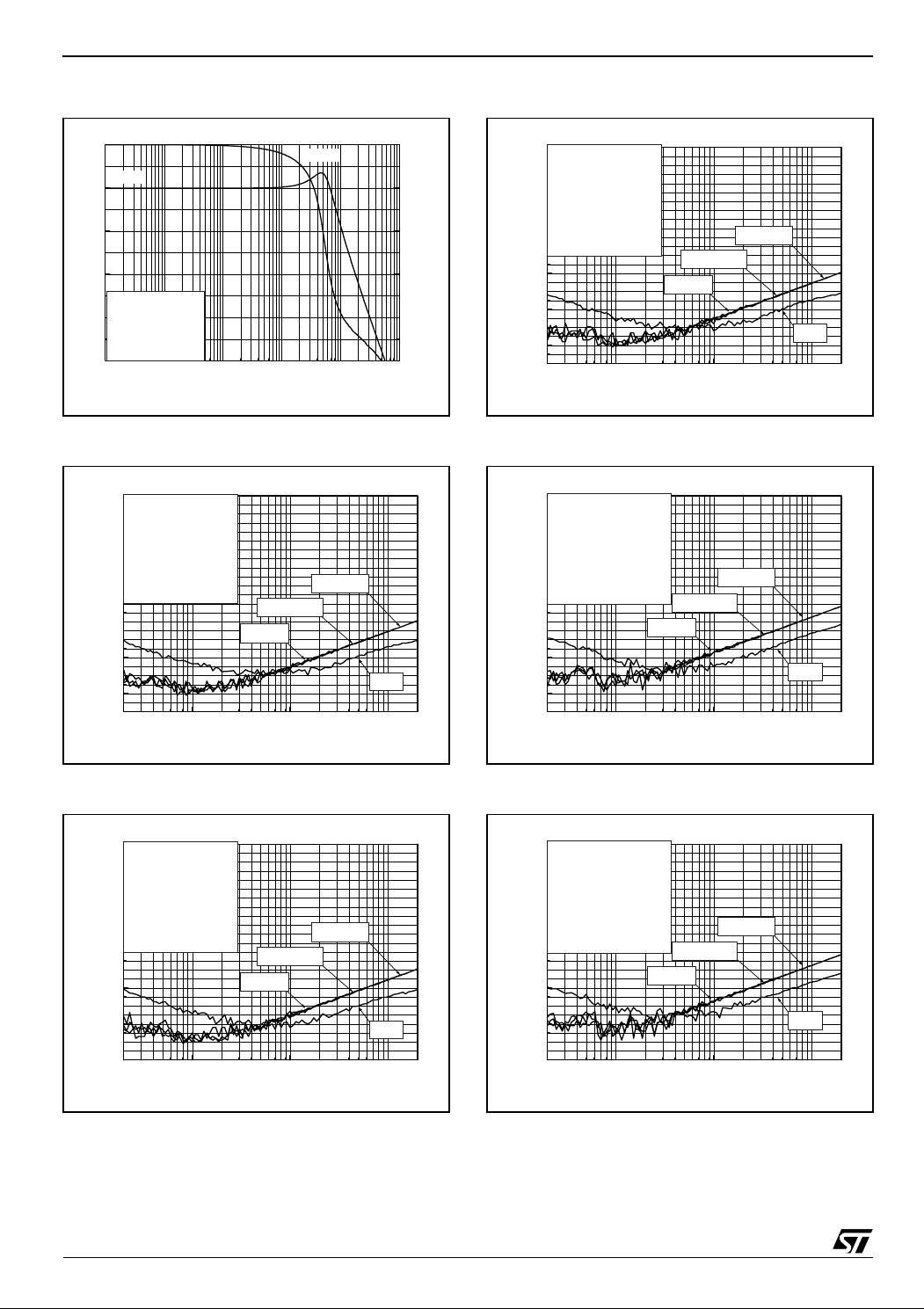
Figure 3. Current consumption vs. power
supply voltage
4.0
No load
Tamb=25°C
3.5
3.0
2.5
2.0
1.5
1.0
Current Consumption (mA)
0.5
0.0
012345
Power Supply Voltage (V)
Figure 4. Current consumption vs. standby
voltage
4.0
3.5
3.0
2.5
2.0
1.5
1.0
Current Consumption (mA)
0.5
0.0
012345
Standby mode=5V
Standby mode=0V
Vcc = 5V
No load
Tamb=25°C
Standby Voltage (V)
Figure 6. Current consumption vs. standby
voltage
Figure 7. Differential DC output voltage vs.
common mode input voltage
1000
Av = 1
Tamb = 25°C
100
10
Voo (mV)
1
0.1
0.01
0.0 0.5 1.0 1.5 2.0 2.5 3.0 3.5 4.0 4.5 5.0
Vcc=2.5V
Common Mode Input Voltage (V)
Vcc=3.3V
Vcc=5V
Figure 5. Current consumption vs. standby
voltage
3.5
3.0
2.5
2.0
1.5
1.0
Current Consumption (mA)
0.5
0.0
0.0 0.6 1.2 1.8 2.4 3.0
Standby mode=0V
Standby mode=3.3V
Standby Voltage (V)
Figure 8. Power dissipation vs. output power
Vcc = 3.3V
No load
Tamb=25°C
7/31

TS4994 Electrical Characteristics
88121616 20 2424 28 3232
0.0
0.2
0.4
0.6
0.8
1.0
Vcc=4.5V
Vcc=5V
Vcc=2.5V
Vcc=3V
Vcc=4V
Vcc=3.5V
THD+N=1%
Cb = 1 F
F = 1kHz
BW < 125kHz
Tamb = 25°C
Output power (W)
Load Resistance
0 25 50 75 100 125
0.0
0.5
1.0
1.5
AMR Value
with 4 layers PCB
DFN10 Package Power Dissipation (W)
Ambiant Temperature ( C)
Figure 9. Power dissipation vs. output power
0.3
RL=8
0.2
0.1
Power Dissipation (W)
0.0
0.0 0.1 0.2 0.3 0.4
RL=16
Ω
Output Power (W)
Ω
Vcc=3.3V
F=1kHz
THD+N<1%
Figure 10. Power dissipation vs. output power
0.20
Vcc=2.6V
F=1kHz
THD+N<1%
0.15
RL=8
Ω
0.10
Figure 12. Output power vs. power supply
voltage
1.50
Cb = 1µF
F = 1kHz
1.25
BW < 125kHz
Tamb = 25°C
1.00
0.75
0.50
0.25
Output power @ 10% THD + N (W)
0.00
2.5 3.0 3.5 4.0 4.5 5.0
Vcc (V)
8
Ω
16
Ω
32
Ω
Figure 13. Output power vs. load resistance
0.05
Power Dissipation (W)
0.00
0.0 0.1 0.2 0.3
RL=16
Output Power (W)
Figure 11. Output power vs. power
supply voltage
1.0
Cb = 1µF
F = 1kHz
0.8
BW < 125kHz
Tamb = 25°C
0.6
0.4
0.2
Output power @ 1% THD + N (W)
0.0
2.5 3.0 3.5 4.0 4.5 5.0
8/31
Vcc (V)
Ω
Figure 14. Power derating curves
8
Ω
16
Ω
32
Ω

Electrical Characteristics TS4994
Figure 15. Power derating curves
0.6
Nominal Value
0.4
0.2
MiniSO8 Package Power Dissipation (W)
0.0
AMR Value
0 25 50 75 100 125
Ambiant Temperature ( C)
Figure 16. Open loop gain vs. frequency
60
Gain
40
20
Gain (dB)
0
Vcc = 5V
-20
ZL = 8Ω + 500pF
Tamb = 25°C
-40
0.1 1 10 100 1000 10000
Phase
Frequency (kHz)
0
-40
-80
-120
-160
-200
Figure 18. Open Loop gain vs. frequency
60
Gain
40
20
Gain (dB)
0
Vcc = 2.6V
-20
ZL = 8Ω + 500pF
Tamb = 25°C
-40
0.1 1 10 100 1000 10000
Phase
Frequency (kHz)
Figure 19. Close loop gain vs. frequency
10
Gain
0
-10
Phase (°)
-20
Gain (dB)
Vcc = 5V
-30
Av = 1
ZL = 8Ω + 500pF
Tamb = 25°C
-40
0.1 1 10 100 1000 10000
Frequency (kHz)
Phase
0
-40
-80
-120
-160
-200
0
-40
-80
-120
-160
-200
Phase (°)
Phase (°)
Figure 17. Open loop gain vs. frequency
60
Gain
40
20
Gain (dB)
0
Vcc = 3.3V
-20
ZL = 8Ω + 500pF
Tamb = 25°C
-40
0.1 1 10 100 1000 10000
Phase
Frequency (kHz)
0
-40
-80
-120
-160
-200
Figure 20. Close loop gain vs. frequency
10
Gain
0
-10
Phase (°)
-20
Gain (dB)
Vcc = 3.3V
-30
Av = 1
ZL = 8Ω + 500pF
Tamb = 25°C
-40
0.1 1 10 100 1000 10000
Frequency (kHz)
Phase
0
-40
-80
-120
-160
-200
Phase (°)
9/31
TS4994 Electrical Characteristics
Figure 21. Close loop gain vs. frequency
10
Gain
0
-10
-20
Gain (dB)
Vcc = 2.6V
-30
Av = 1
ZL = 8Ω + 500pF
Tamb = 25°C
-40
0.1 1 10 100 1000 10000
Frequency (kHz)
Phase
Figure 22. PSRR vs. frequency
0
-10
Vcc = 5V
Vripple = 200mVpp
-20
Inputs = Grounded
-30
Av = 1, Cin = 4.7µF
-40
RL ≥ 8
PSRR (dB)
-50
-60
-70
-80
-90
-100
-110
-120
Tamb = 25°C
20
Ω
Cb=0.47µF
Cb=1µF
100 1000 10000
Frequency (Hz)
Cb=0.1µF
Cb=0
0
-40
-80
-120
-160
-200
20k
Figure 24. PSRR vs. frequency
0
-10
Vcc = 2.6V
Vripple = 200mVpp
-20
Inputs = Grounded
-30
Av = 1, Cin = 4.7µF
-40
RL ≥ 8
Tamb = 25°C
20
Ω
100 1000 10000
-50
Phase (°)
PSRR (dB)
-60
-70
-80
-90
-100
-110
-120
Figure 25. PSRR vs. frequency
0
-10
Vcc = 5V
Vripple = 200mVpp
-20
Inputs = Grounded
-30
Av = 2.5, Cin = 4.7µF
-40
RL ≥ 8
Tamb = 25°C
20
Ω
100 1000 10000
PSRR (dB)
-50
-60
-70
-80
-90
-100
-110
-120
Cb=0.47µF
Cb=1µF
Frequency (Hz)
Cb=0.47µF
Cb=1µF
Frequency (Hz)
Cb=0.1µF
Cb=0
20k
Cb=0.1µF
Cb=0
20k
Figure 23. PSRR vs. frequency
0
-10
Vcc = 3.3V
Vripple = 200mVpp
-20
Inputs = Grounded
-30
Av = 1, Cin = 4.7µF
-40
RL ≥ 8
Tamb = 25°C
20
Ω
Cb=0.47µF
Cb=1µF
100 1000 10000
Frequency (Hz)
10/31
PSRR (dB)
-50
-60
-70
-80
-90
-100
-110
-120
Cb=0.1µF
Cb=0
20k
Figure 26. PSRR vs. frequency
0
-10
Vcc = 3.3V
Vripple = 200mVpp
-20
Inputs = Grounded
-30
Av = 2.5, Cin = 4.7µF
-40
RL ≥ 8
PSRR (dB)
-50
-60
-70
-80
-90
-100
-110
-120
Tamb = 25°C
20
Ω
Cb=1µF
100 1000 10000
Frequency (Hz)
Cb=0.1µF
Cb=0.47µF
Cb=0
20k
 Loading...