

STMicroelectronics TS461, TS462, TS464 Operation Manual
TS461-TS462-TS464
Output Rail-to-Rail Operational Amplifiers
■ High dynamic features
■ Large output swing (±2.4V @ V
= ±2.5V)
CC
■ Low noise level: 4nV/√Hz
■ Low distortion: 0.003%
■ Operating range: 2.7V to 10V
■ Available in SOT23-5 micropackage
Description
The TS46x are a family of operational amplifiers
able to operate with voltages as low as ±1.35V
and to reach a minimum of ±2Vpp of output
swing when supplied with ±2.5V.
This device is well-suited for all kinds of portable
and battery-supplied equipment, where low noise
and low distortion are key requirements.
The TS461/2/4 offer excellent output rail-to-rail
performance at an attractive cost.
Applications
■ Sound cards
■ PDA
■ CD players
■ Recording equipment
■ Multimedia
■ Microphone preamplifiers
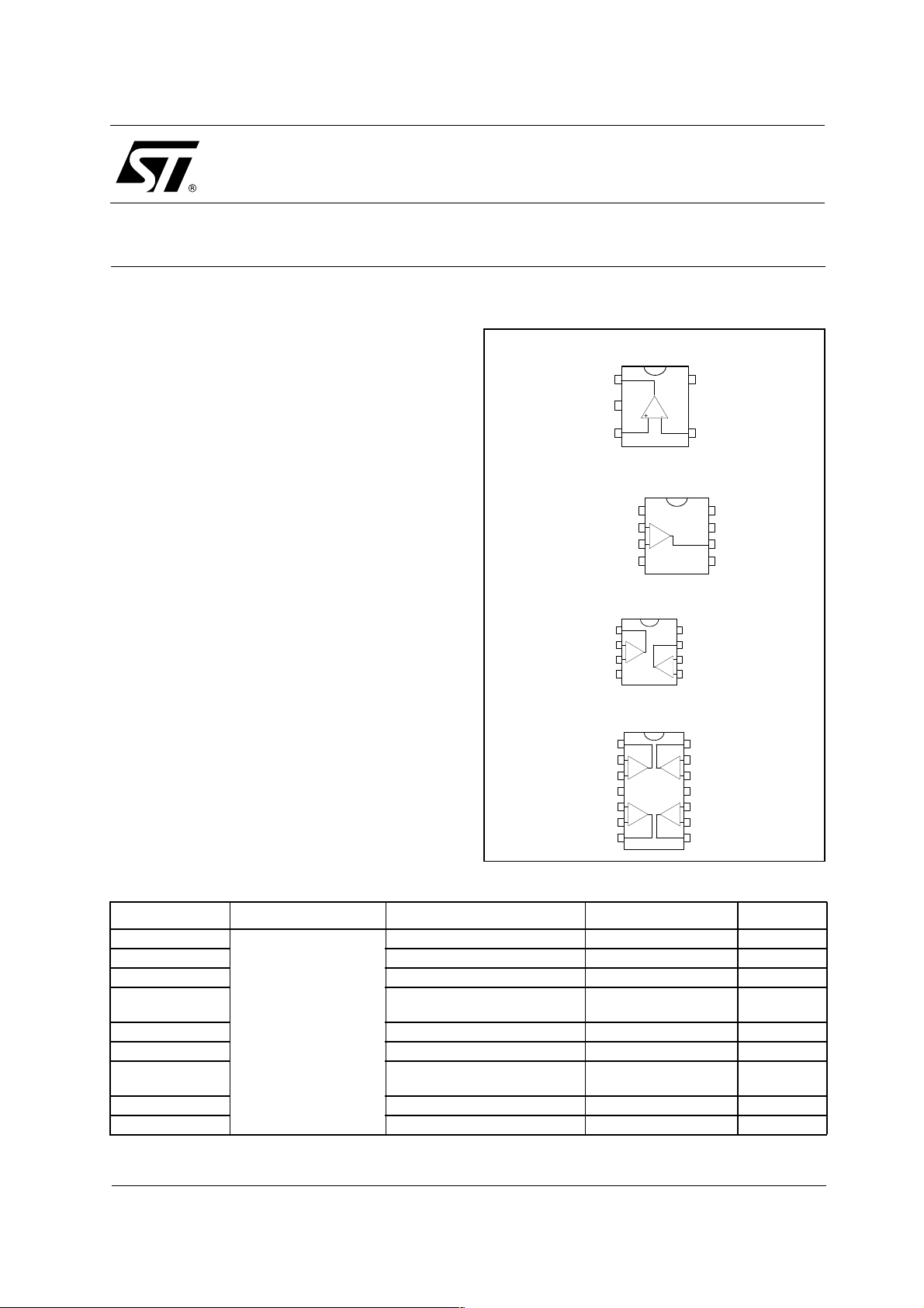
Pin Connections (top view)
TS461CLT
8
7
-
6
+
-
+
+
-
V
5
Inverting input
4
V
CC
Output 2
Inverting Input 2
Non-inverting Input 2
14
Output 4
13
Inverting Input 4
12
Non-inverting Input 4
11
V
DD
10
Non-inverting Input 3
9
Inverting Input 3
8
Output 3
Output
1
V
2
DD
Non-inverting input
3
TS461CD
1
N.C.
Inverting Input 1
Non-inverting Input 1
2
-
+
3
V
4
DD
TS462CN-TS462CD-TS462CPT-TS462CST
Inverting Input 1
Non-inverting Input 1
-
2
+
3
V
45
DD
1
Output 1
TS464CN-TS464CD-TS464CPT
Output 1
Output 2
V
1
2
-
+
3
4
CC
5
+
-
6
7
Inverting Input 1
Non-inverting Input 1
Non-inverting Input 2
Inverting Input 2
CC
N.C.
8
V
7
CC
6
Output 2
N.C.
5
Order Codes
Part Number Temperature Range Package Packaging Marking
TS461CLT
TS461CD/CDT SO-8 Tube or Tape & Reel
TS462CST mini SO-8 Tape & Reel
TS462CPT
TS462CN DIP8 Tube
-20°C, +70°C
(Thin Shrink Outline Package)
TS462CD/CDT SO-8 Tube or Tape & Reel
TS464CPT
(Thin Shrink Outline Package)
TS464CN DIP14 Tube
TS464CD/CDT SO-14 Tube or Tape & Reel
March 2005 Revision 2 1/12
SOT23-5L Tape & Reel K105
TSSOP-8
TSSOP-14
Tape & Reel
Tape & Reel
Absolute Maximum Ratings TS461-TS462-TS464
1 Absolute Maximum Ratings
Table 1: Key parameters and their absolute maximum ratings
Symbol Parameter Value Unit
VCC
Vid
T
T
R
Supply voltage
Differential Input Voltage
V
Input Voltage Range Vdd-0.3 to Vcc+0.3
in
Operating Free Air Temperature Range
oper
Storage Temperature Range
std
Maximum Junction Temperature
T
j
Thermal Resistance Junction to Case
thja
SOT23-5
SO8
SO14
TSSOP8
TSSOP14
HBM: Human Body Model
ESD
MM: Machine Model
CDM: Charged Device Model 1.5 kV
Lead Temperature (soldering, 10sec) 250 °C
1) All voltages values, except differential voltage are with respect to network group terminal.
2) Differential voltages are non-inverting input terminal with respect to the inverting input termin al.
3) Short-circuits can cause excessive heating and destructive dissipation.
4) Human body model, 100pF discharged through a 1.5kΩ resistor into pin of device.
5) Machine model ESD, a 200pF cap is charged to the specified voltage, then discharged directly into the IC with no external series resistor
(internal resistor < 5
Table 2: Operating conditions
1
2
4
5
Ω), into pin to pin of device.
12 V
±VCC V
V
-20 to +70 °C
-65 to +150 °C
150 °C
3
°C/W
250
125
103
120
100
2kV
200 V
Symbol Parameter Value Unit
VCC Supply Voltage 2.7 to 10 V
Vicm
T
oper
Common Mode Input Voltage Range V
Operating Free Air Temperature Range
+1.15 to VCC - 1.15
DD
-20 to +70 °C
V
2/12
TS461-TS462-TS464 Electrical Characteristics
2 Electrical Characteristics
Table 3: VCC = 2.5V, VDD = -2.5V, T
Symbol Parameter Min. Typ. Max. Unit
= 25°C (unless otherwise specified)
amb
V
io
∆V
I
io
I
ib
V
icm
CMR
SVR
A
vd
V
OH
V
OL
I
CC
GBP
SR
en
Input Offset Voltage
T
≤ T
min.
Input Offset Voltage Drift
io
V
= 0V, Vo = 0V
icm
amb
≤ T
max.
Input Offset Current
V
= 0V, Vo = 0V
icm
≤ T
T
min.
amb
≤ T
max.
Input Bias Current
V
= 0V, Vo = 0V
icm
≤ T
T
min.
amb
≤ T
max.
Common Mode Input Voltage Range
Common Mode Rejection Ratio
= ±1.35V
V
icm
Supply Voltage Rejection Ratio
= ±2V to ±3V
V
cc
Large Signal Voltage Gain RL = 2kΩ
High Level Output Voltage RL = 2kΩ
Low Level Output Voltage RL = 2kΩ
Supply Current, per amplifier
Unity gain - no load 2 2.8
Gain Bandwidth Product
f = 100kHz R
Slew Rate
= 1, Vin = ±1V
A
V
Equivalent Input Noise Voltage
f = 100kHz
= 2kΩ, CL = 100pF
L
157mV
µV/°C
5
nA
10 150
200
nA
200
200
750
1000
-1.35 1.35 V
dB
60 85
dB
60 70
70 80 dB
22.4 V
-2.4 -2 V
mA
MHz
8.5 12
V/
µs
2.8 4
nV
4
-----------Hz
3/12
THD
Total Harmonic Distortion
f = 1kHz, A
= -1 RL = 10kΩ
V
0.003
%
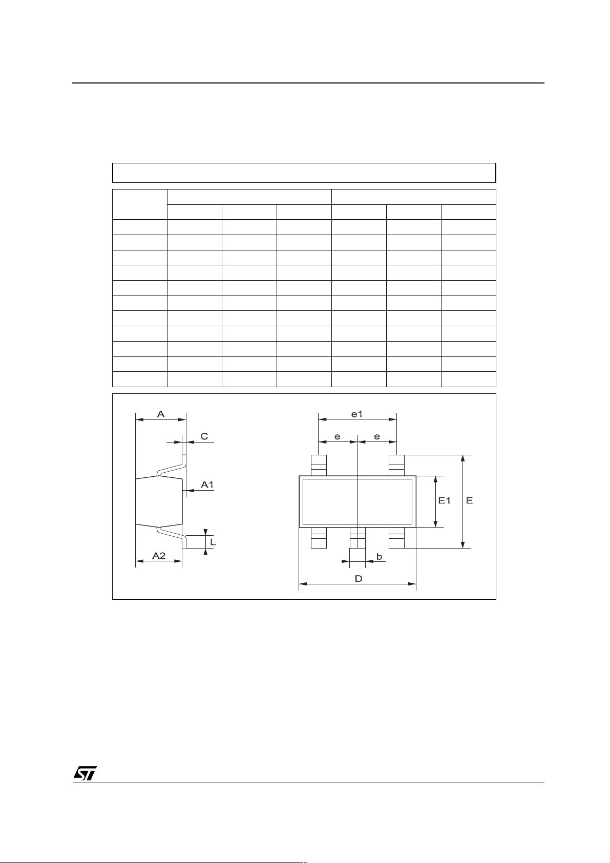
Package Mechanical Data TS461-TS462-TS464
3 Package Mechanical Data
3.1 SOT23-5L package
SOT23-5L MECHANICAL DATA
DIM.
A 0.90 1.45 35.4 57.1
A1 0.00 0.15 0.0 5.9
A2 0.90 1.30 35.4 51.2
b 0.35 0.50 13.7 19.7
C 0.09 0.20 3.5 7.8
D 2.80 3.00 110.2 118.1
E 2.60 3.00 102.3 118.1
E1 1.50 1.75 59.0 68.8
e.95 37.4
e1 1.9 74.8
L 0.35 0.55 13.7 21.6
MIN. TYP MAX. MIN. TYP. MAX.
mm. mils
0
4/12
 Loading...