

STMicroelectronics TS4601B Technical data
Features
TS4601B
High performance stereo headphone amplifier
with capacitorless outputs and I
2
C bus interface
■ Power supply range: 2.9 V to 5.5 V
■ 107 dB of PSRR at 217 Hz
■ Fully differential inputs
■ I²C interface for volume control
■ Digital volume control range from -60 dB to
+4 dB
■ 101 dB of SNR A-weighted
■ Independent right and left channel shutdown
control
■ Low quiescent current: 4.8 mA typ. at 3.0 V
■ Low standby current: 2 µA max
■ Output-coupling capacitors removed
■ Flip-chip package 2.1 mm x 2.1 mm, 500 µm
pitch, 16 bumps
Applications
■ Cellular phones
■ Notebook computers
■ CD/MP3 players
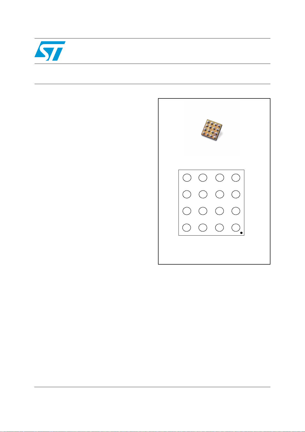
TS4601BEIJT - Flip-chip
Pinout (top view)
SDA
SDZ
SDZ
INR-
INR-
INL-
INL-
SDA
INR+
INR+
INL+
INL+
GND
GND
4321
4321
SCL
SCL
CMS
CMS
PVSS
PVSS
C1
C1
VOUTR
VOUTR
VCC
VCC
VOUTL
VOUTL
C2PVCC
C2PVCC
D
D
C
C
B
B
A
A
Balls are underneath
Description
The TS4601B is a stereo headphone driver
dedicated to high audio performance and spaceconstrained applications. It has the same uses as
the TS4601 which it replaces, while offering highly
improved ESD ratings.
It is based on low power dissipation amplifier core
technology. Special care was taken in the design
of the amplification chain to achieve peerless
PSRR (107 dB typ. at 217 Hz) and 101 dB of
SNR.
The TS4601B can drive 0.9 V
into 16 Ω and 1.6 V
into 10 kΩ, whatever the
rms
output voltage
rms
An I²C interface offers volume control in 64 steps
from -60 dB to +4 dB and multiple configuration
modes for the device.
The traditionally used output-coupling capacitors
can be removed and a dedicated common-mode
sense pin removes parasitic noise from the jack.
The TS4601B is designed to be used with an
output serial resistor. It ensures unconditional
stability over a wide range of capacitive loads.
The TS4601B is packaged in a tiny 16-bump flipchip with a pitch of 500 µm and a 300 µm
diameter ball size.
power supply voltage, in the 2.9 V to 5.5 V range.
July 2008 Rev 2 1/28
www.st.com
28

Contents TS4601B
Contents
1 Absolute maximum ratings and operating conditions . . . . . . . . . . . . . 3
2 Typical application schematics . . . . . . . . . . . . . . . . . . . . . . . . . . . . . . . . 4
3 Electrical characteristics . . . . . . . . . . . . . . . . . . . . . . . . . . . . . . . . . . . . . 6
3.1 Electrical characteristics tables . . . . . . . . . . . . . . . . . . . . . . . . . . . . . . . . . 6
3.2 Electrical characteristic curves . . . . . . . . . . . . . . . . . . . . . . . . . . . . . . . . . . 8
4 Application information . . . . . . . . . . . . . . . . . . . . . . . . . . . . . . . . . . . . . 17
4.1 Common-mode sense . . . . . . . . . . . . . . . . . . . . . . . . . . . . . . . . . . . . . . . 17
4.2 I²C bus interface . . . . . . . . . . . . . . . . . . . . . . . . . . . . . . . . . . . . . . . . . . . . 17
4.2.1 I²C bus operation . . . . . . . . . . . . . . . . . . . . . . . . . . . . . . . . . . . . . . . . . . 17
4.2.2 Control registers . . . . . . . . . . . . . . . . . . . . . . . . . . . . . . . . . . . . . . . . . . 19
Control register CR0 . . . . . . . . . . . . . . . . . . . . . . . . . . . . . . . . . . . . . . . . . . . . . . . 21
4.3 Wake-up and standby time definition . . . . . . . . . . . . . . . . . . . . . . . . . . . . 22
4.4 Decoupling considerations . . . . . . . . . . . . . . . . . . . . . . . . . . . . . . . . . . . . 22
4.5 Low frequency response . . . . . . . . . . . . . . . . . . . . . . . . . . . . . . . . . . . . . 23
4.6 Low pass output filter . . . . . . . . . . . . . . . . . . . . . . . . . . . . . . . . . . . . . . . . 23
4.7 Single-ended input configuration . . . . . . . . . . . . . . . . . . . . . . . . . . . . . . . 24
5 Package information . . . . . . . . . . . . . . . . . . . . . . . . . . . . . . . . . . . . . . . . 25
6 Ordering information . . . . . . . . . . . . . . . . . . . . . . . . . . . . . . . . . . . . . . . 27
7 Revision history . . . . . . . . . . . . . . . . . . . . . . . . . . . . . . . . . . . . . . . . . . . 27
2/28
TS4601B Absolute maximum ratings and operating conditions
1 Absolute maximum ratings and operating conditions
Table 1. Absolute maximum ratings
Symbol Parameter Value Unit
V
CC
Supply voltage
Input voltage
V
in
In Master standby mode, and I²C mode 1, 6
and 7
In I²C mode 2, 3, 4 and 5
T
stg
T
R
thja
P
d
Storage temperature -65 to +150 °C
Maximum junction temperature 150 °C
j
Thermal resistance junction to ambient
Power dissipation Internally limited
HBM - human body model - all pins
VOUTL, VOUTR vs. VCC, GND
MM - machine model (min. value)
ESD
CDM - charge device model 500 V
IEC61000-4-2 level 4, contact
IEC61000-4-2 level 4, air discharge
Latch-up Latch-up immunity 200 mA
Lead temperature (soldering, 10sec) 260 °C
(1)
(6)
(5)
(4)
(6)
(2)
6V
0 to V
CC
V
-2.4 to +2.4
200 °C/W
(3)
2
4
kV
200 V
+/- 8
+/- 15
kV
1. All voltage values are measured with respect to the ground pin.
2. The device is protected in case of over temperature by a thermal shutdown active @ 150° C.
3. Exceeding the power derating curves during a long period may provoke abnormal operation.
4. Human body model: A 100 pF capacitor is charged to the specified voltage, then discharged through a
1.5 kΩ resistor between two pins of the device. This is done for all couples of connected pin combinations
while the other pins are floating.
5. Machine model: A 200 pF capacitor is charged to the specified voltage, then discharged directly between
two pins of the device with no external series resistor (internal resistor < 5 Ω). This is done for all couples of
connected pin combinations while the other pins are floating.
6. The measurement is performed on the evaluation board, with an STMicroelectronics ESD protection
EMIF02-AV01F3
Table 2. Operating conditions
Symbol Parameter Value Unit
V
T
R
CC
R
C
oper
thja
Supply voltage 2.9 to 5.5 V
Load resistor ≥ 16 Ω
L
L
Load capacitor
Serial resistor of 12Ω minimum, R
≥ 16Ω,
L
0.8 to 100 nF
Operating free air temperature range -40 to +85 °C
Flip-chip thermal resistance junction to ambient 90 °C/W
3/28
Typical application schematics TS4601B
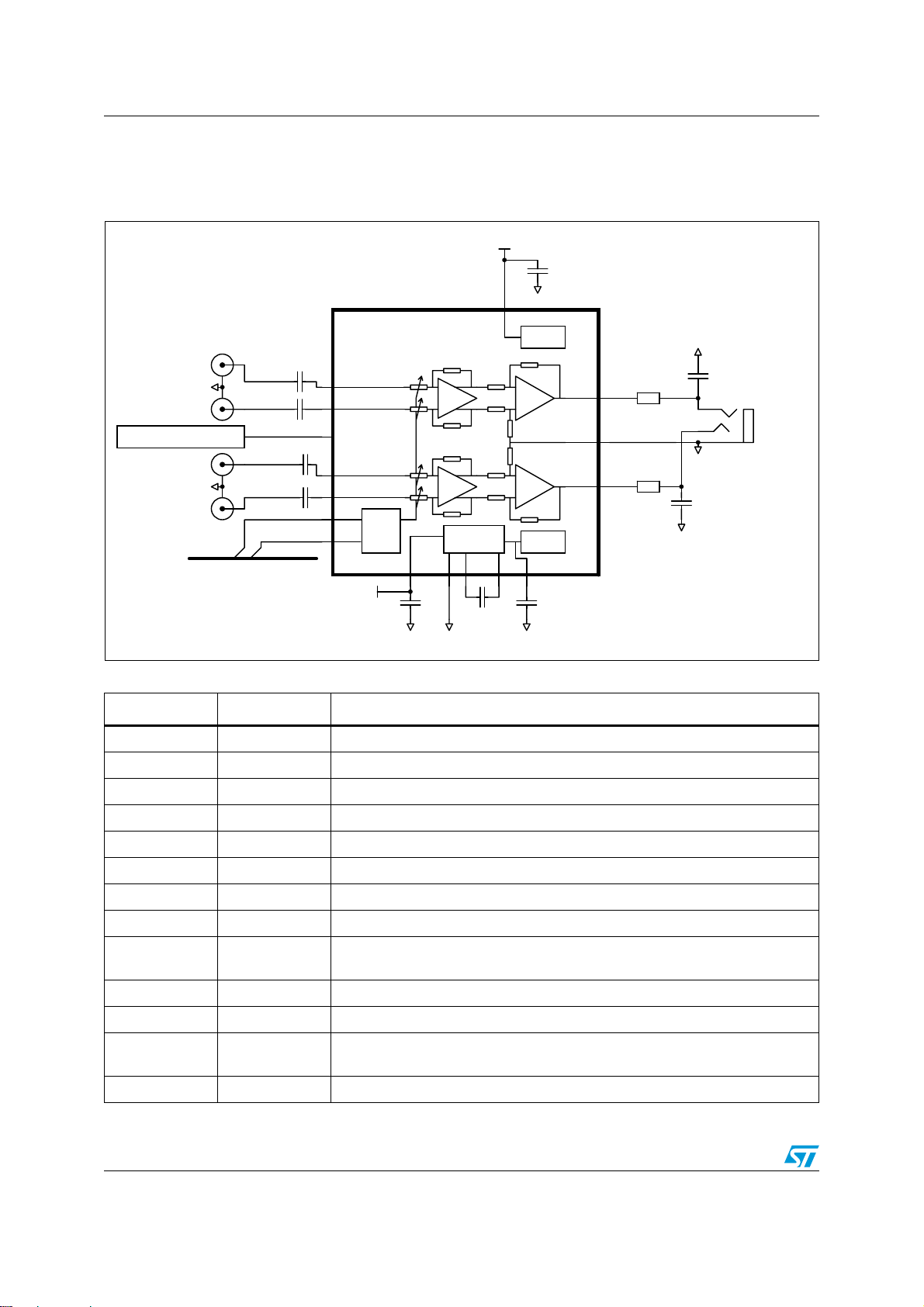
2 Typical application schematics
Figure 1. Typical application schematics for the TS4601B
Vcc
Cs
1uF
Vcc
Gnd
C1
Positive
Reg
-
+
+
-
Negative
Reg
PVss
B2
Css
2.2uF
VoutL
CMS
VoutR
12 ohms min.
B1
C2
12 ohms min.
D1
Rout
Rout
Gnd
Gnd
Gnd
Cout
0.8nF min.
Cout
0.8nF min.
Headphone / Line Out
Negative Left Input
Gnd
Positive Left Input
Master Standby Command
Positive Right Input
Gnd
Negative Right Input
I2C Bus
Cin
2.2uF
Cin
2.2uF
Cin
2.2uF
Cin
2.2uF
B4
B3
D4
C3
C4
D3
D2
TS4601
InL-
InL+
SDZ
InR+
InR-
SDA
SCL
-
+
+
-
I2C
PVcc Gnd C1 C2
A4 A3 A2 A1
Vcc
Cs
1uF
Gnd GndGnd
Negative
Supply
C12
1uF
Table 3. Pin description for the TS4601B
Pin number Pin name Pin definition
C1 VCC Analog supply voltage, connect to V
A4 PVCC Power supply voltage, connect to V
battery
battery
A2 C1 Capacitor terminal for internal negative supply generator.
A1 C2 Capacitor terminal for internal negative supply generator.
B2 PVSS Capacitor terminal for internal negative supply generator filtering.
D1 VOUTR Right audio channel output signal.
B1 VOUTL Left audio channel output signal.
A3 GND Ground of the device.
C2 CMS
Common-mode sense, to be connected as close as possible to the ground of
headphone / line out plug.
B4 INL- Left audio channel negative input signal.
B3 INL+ Left audio channel positive input signal.
D4 SDZ
Master standby of the circuit. When SDZ = 0, the device is also reset to initial
state. Up to V
tolerant input.
CC
C4 INR- Right audio channel negative input signal.
.
.
4/28
TS4601B Typical application schematics
Table 3. Pin description for the TS4601B (continued)
Pin number Pin name Pin definition
C3 INR+ Right audio channel positive input signal.
D3 SDA I²C signal data. Up to V
D2 SCL I²C clock signal. Up to V
tolerant input.
CC
tolerant input.
CC
Table 4. Component description for the TS4601B
Component Value Description
and PVCC. Two 1µF capacitors are enough for
CC
Cs 1µF
C12 1µF
C
SS
C
in
C
out
R
out
2.2µF
Cin
------------------------=
2πZinFc
0.8nF to 100nF
12Ω min.
Decoupling capacitors for V
proper decoupling of TS4601B. X5R dielectric and 10V rating voltage is
recommended to minimize ΔC/ΔV when V
Must be placed as close as possible to the TS4601B to minimize parasitic
inductance and resistance.
Capacitor for internal negative power supply operation. X5R dielectric and 10V
rating voltage is recommended to minimize ΔC/ΔV when VCC=5V.
Must be placed as close as possible to the TS4601B to minimize parasitic
inductance and resistance.
Filtering capacitor for internal negative power supply. X5R dielectric and 10V
rating voltage is recommended to minimize ΔC/ΔV when V
1
Input coupling capacitor that forms with Zin, a first order high pass filter with a
-3dB cut-off frequency FC. Zin is 12kΩ typical and independent of the gain
setting.
For example F
= 13Hz, Cin = 1µF and for FC = 6Hz, Cin = 2.2µF
C
Output capacitor of 0.8nF minimum to 100nF maximum. This capacitor is
mandatory for operation of the TS4601B.
Output resistor in series with the TS4601B output. This 12Ω minimum resistor
is mandatory for operation of the TS4601B.
CC
=5V.
CC
= 5V.
5/28
Electrical characteristics TS4601B
3 Electrical characteristics
3.1 Electrical characteristics tables
Table 5. Electrical characteristics of the I²C interface
from V
=+2.9 V to VCC=+5.5 V, GND = 0 V, T
CC
= 25° C (unless otherwise specified)
amb
Symbol Parameter Min. Typ. Max. Unit
V
V
V
V
F
SCL
V
OL
I
in
Table 6. Electrical characteristics of the amplifier
Low level input voltage on SDZ pins 0.63 V
IL
High level input voltage on SDZ pins 1.1 V
IH
Low level input voltage on SDA, SCL pins 0.6 V
IL
High level input voltage on SDA, SCL pins 1.3 V
IH
I2C clock frequency 400 kHz
Low level output voltage, SDA pin, I
= 3mA 0.4 V
sink
Input current on SDA, SCL from 0.4V to 4.5V 10 µA
from V
=+2.9 V to VCC=+5.5 V, GND = 0 V, T
CC
= 25° C (unless otherwise specified)
amb
Symbol Parameter Min. Typ. Max. Unit
Quiescent supply current, no input signal, both channels
I
CC
enabled, RL= 16Ω
= 3.0V
V
CC
VCC = 5.0V
4.8
5.6
6
7
Master standby current, No input signal
I
STBY
I
STBY
= 0V
V
SDZ
V
= 0.35V, VCC= 5V
SDZ
0.5 2
10
I²C standby current, no input signal 75 µA
Pull-down resistor on SDZ 480 600 720 kΩ
V
V
oo
Input differential voltage range
in
Output offset voltage
No input signal, RL = 32Ω
(1)
1.2 V
-5 +5 mV
mA
µA
rms
Maximum output voltage, in-phase signals
V
out
Frequency
range
= 16Ω, THD+N = 1% max, f = 1kHz
R
L
= 10kΩ, Rs=15Ω, CL=1nF, THD+N = 1% max, f = 1kHz
R
L
RL = 16Ω, G = 0dB, P
= 20mW, +/- 0.5dB (related to1kHz)
out
Cin = 4.7µF
Total harmonic distortion + noise, G = 0dB
THD + N
R
= 16Ω, Po = 5mW, F = 1kHz
L
= 16Ω, Po = 10mW, 20Hz < F < 20kHz 0.2
R
L
6/28
0.9
V
1.6
10 22000 Hz
0.02 %
rms
TS4601B Electrical characteristics
Table 6. Electrical characteristics of the amplifier
from V
Symbol Parameter Min. Typ. Max. Unit
Power supply rejection ratio
F = 217Hz, R
PSRR
CMRR
Crosstalk
SNR
ONoise
G Gain range with Gain(dB) = 20xlog[(V
Mute InL/R+ - InL/R- = 1V
-
- Step size error -1 +1 stepsize
V
F = 10kHz, R
V
Common mode rejection ratio
= 16Ω, F = 20Hz to 20 kHz, G = 0dB, Vic = 200 mV
R
L
Channel separation
R
RL = 10kΩ, G = 0dB, F = 1kHz, V
Signal to noise ratio, A-weighted, R
THD+N < 1%, F = 1kHz, G=+4 dB
Output noise voltage, A-weighted
G= +4dB
G=-19.5dB -103
Gain step size
from -60dB to -36dB
from -36dB to -16.5dB
from -16.5dB to +4dB
Gain error (G = +4dB) -0.45 +0.42 dB
=+2.9 V to VCC=+5.5 V, GND = 0 V, T
CC
(2)
= 16Ω, G = 0dB
= 200mVpp, grounded inputs
ripple
= 200 mVpp, grounded inputs
ripple
= 16Ω, G = 0dB, F = 1kHz, Po = 40mW
L
L
= 16Ω, G = 0dB
L
rms
= 1.6V
out
=16 Ω, V
L
(3)
(3)
L/R)/(InL/R+ - InL/R-)] -60 +4 dB
out
rms
= 0.9V
out
= 25° C (unless otherwise specified)
amb
100
107
70
65 dB
pp
60
80
rms
82
84
101 dB
-100
-80 dB
3
1.5
0.5
dB
dB
dBV
dB
Left and right channel input impedance all gains setting
Z
in
Single-ended inputs referenced to GND
Differential inputs
Output impedance in Mode 5 (negative supply is ON and
amplifier output stages are OFF)
Z
out
F < 40kHz
F = 6MHz
F = 36MHz
t
wu
t
STBY
1. Guaranteed by design and parameter correlation.
2. Dynamic measurements - 20*log(rms(V
3. Guaranteed by design and parameter correlation.
Wake-up time 12 22 ms
Standby time 10 µs
)/rms(V
out
(3)
ripple
10
20
12
24
14.5
29
10
500
75
)). V
is an added sinus signal to VCC @ F = 217 Hz.
ripple
7/28
kΩ
kΩ
Ω
Ω

Electrical characteristics TS4601B
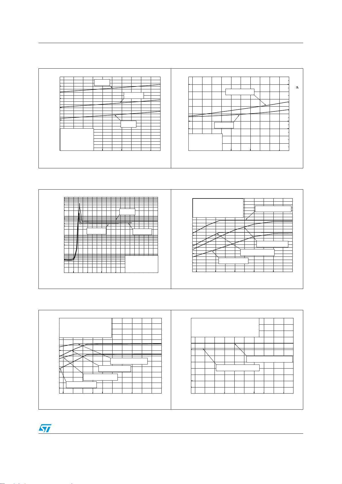
3.2 Electrical characteristic curves
Current consumption vs. power supply voltage see Figure 2
Standby current consumption vs. power supply voltage see Figure 3 and Figure 4
Maximum output power vs. power supply voltage see Figure 5
Maximum output power vs. power supply voltage see Figure 6
Maximum output voltage vs. power supply voltage see Figure 7
PSRR vs. frequency see Figure 8 to Figure 12
PSRR vs. gain setting see Figure 13
THD+N vs. output power see Figure 14 to Figure 25
THD+N vs. output voltage see Figure 26
THD+N vs. frequency see Figure 27
THD+N vs. frequency see Figure 28 to Figure 39
CMRR vs. frequency see Figure 40 and Figure 41
Crosstalk vs. frequency see Figure 42 to Figure 45
Common mode response vs. frequency see Figure 46
THD+N vs. input voltage. Line in mode 5 see Figure 47
Input impedance vs. frequency. Line in mode 5 see Figure 48
Gain vs. frequency see Figure 49
Note: When the label “RC network” is present in a curve, it means that a 12 Ω + 1 nF low pass filter
connected on outputs is used (refer to Figure 1: Typical application schematics for the
TS4601B on page 4).
8/28
TS4601B Electrical characteristics
3.0 3.5 4.0 4.5 5.0 5.5
0
25
50
75
100
125
150
175
200
225
250
275
300
THD+N=10% (180°)
THD+N=10% (0°)
THD+N=1% (0°)
RL = 16Ω, F = 1kHz
Left & Right
BW < 30kHz, Tamb = 25°C
THD+N=1% (180°)
Output power (mW)
Vcc (V)
3.0 3.5 4.0 4.5 5.0 5.5
0.0
0.5
1.0
1.5
2.0
2.5
3.0
THD+N=10% (0° & 180°)
RL = RC network + 10kΩ, F = 1kHz
Left & Right
BW < 30kHz, Tamb = 25°C
THD+N=1% (0° & 180°)
Output Voltage (Vrms)
Vcc (V)
Figure 2. Current consumption vs. power
supply voltage
6.0
5.5
5.0
4.5
4.0
3.5
3.0
2.5
2.0
1.5
No load
Current Consumption (mA)
SDZ = Vcc
1.0
SDA = SCL = Vcc
0.5
Ta = 25°C
0.0
3.0 3.5 4.0 4.5 5.0 5.5
Mode 4
Mode 2, 3
Mode 5
Power Supply Voltage (V)
Figure 4. Standby current consumption vs.
standby voltage
1E-3
1E-4
Vcc=5V
Figure 3. Standby current consumption vs.
power supply voltage
1000
800
600
400
200
No load
SDA = SCL = Vcc
Current Consumption SDZ=Gnd (nA)
Ta = 25°C
0
3.0 3.5 4.0 4.5 5.0 5.5
Mode 1, 6, 7, 8
SDZ=Gnd
Power Supply Voltage (V)
100
90
80
70
60
50
40
30
20
10
0
Figure 5. Maximum output power vs. power
supply voltage
Current Consumption SDZ=Vcc ( A)
1E-5
1E-6
Current Consumption (nA)
1E-7
0.0 0.5 1.0 1.5 2.0 2.5 3.0 3.5 4.0 4.5 5.0
Vcc=2.9V
Figure 6. Maximum output power vs. power
supply voltage
175
RL = 32Ω, F = 1kHz
Left & Right
150
BW < 30kHz, Tamb = 25°C
125
100
75
50
Output power (mW)
25
0
3.0 3.5 4.0 4.5 5.0 5.5
THD+N=1% (180°)
THD+N=1% (0°)
SDZ Voltage (V)
THD+N=10% (180°)
THD+N=10% (0°)
Vcc (V)
Vcc=3.6V
No load
SDA = SCL = Vcc
Ta = 25°C
Figure 7. Maximum output voltage vs. power
supply voltage
9/28
 Loading...