

STMicroelectronics TS393 Technical data
Micropower Dual CMOS Voltage Comparators
1
2
3
45
6
7
8
Inverting Input 2
Output 2
Non-inverting Input 2
Output 1
Inverting Input 1
Non-inverting Input 1
CC
+
V
-
CC
V
-
+
-
+
■ Extremely low supply current: 9µa typ/comp.
■ Wide single supply range 2.7V to 16V or dual
supplies (±1.35V to ±8V)
■ Extremely low input bias current: 1pA typ.
■ Extremely low input offset current: 1pA typ.
■ Input common-mode voltage range includes
GND
■ High input impedance: 10
■ Fast response time: 2.5µs typ. for 5mV
overdrive
■ Pin-to-pin and functionally compatible with
bipolar LM393
Description
The TS393 is a micropower CMOS dual voltage
comparator with extremely low consumption of
9µA typ / comparator (20 times less than bipolar
LM339). Similar performances are offered by the
quad micropower comparator TS3702 with a
push-pull CMOS output.
12
Ω typ
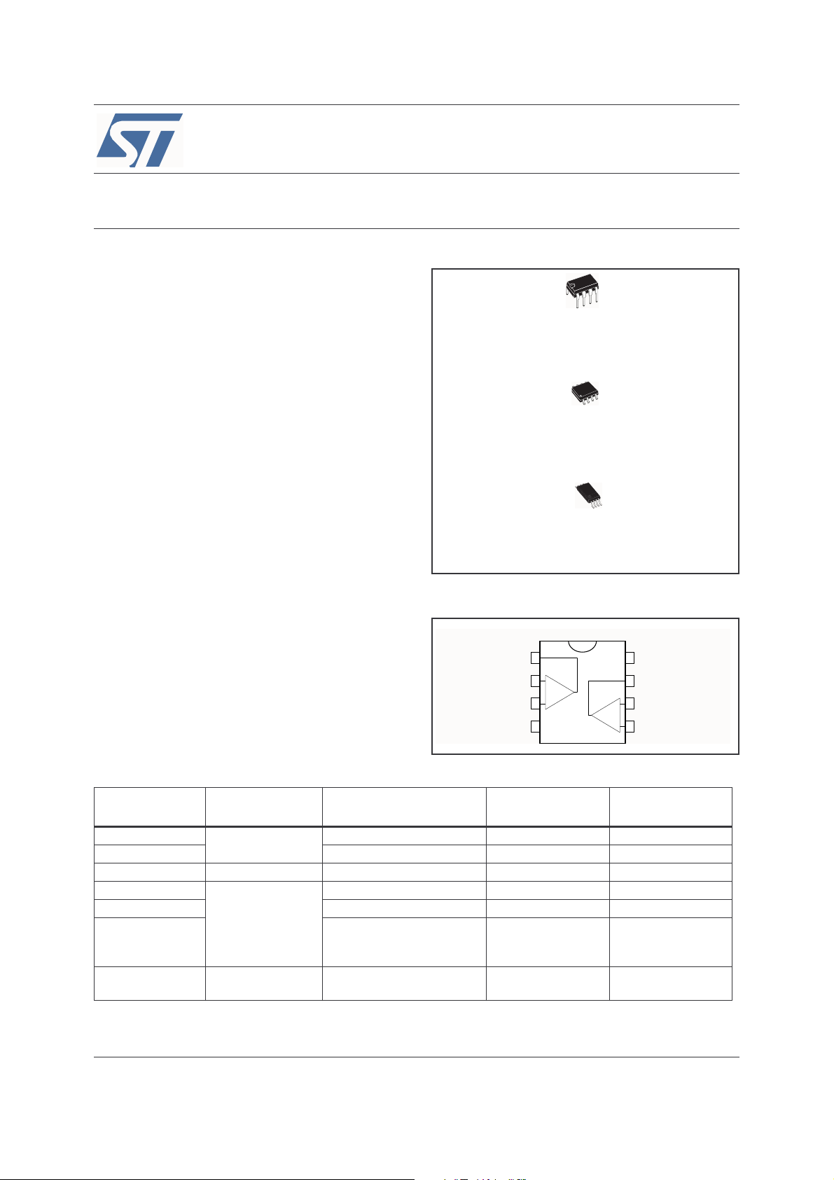
TS393
N
DIP8
(Plastic Package)
D
SO-8
(Plastic Micropackage)
P
TSSOP8
(Thin Shrink Small Outline Package)
Pin Connection (top view)
Thus response times remain similar to the LM393.
Order Codes
Par t Nu mber
TS393CN
TS393CD/CDT SO-8 Tube or Tape & Reel S399C
TS393MD/MDT -55°C, +125°C SO-8 Tube or Tape & Reel S393M
TS393IN
TS393ID/IDT SO-8 Tube or Tape & Reel S393I
TS393IPT
TS393IYD/IYDT -40°C, +125°C
August 2005 1/9
Temperature
Range
0°C, +70°C
Package Packaging Marking
DIP84 Tube TS393CN
DIP8 Tube TS393IN
-40°C, +125°C
TSSOP8
(Thin Shrink Outline
Tape & Reel S393I
Package)
SO-8 (automotive grade
level)
Tube or Tape & Reel S393IY
Rev 2
www.st.com
9
Absolute Maximum Ratings TS393
1 Absolute Maximum Ratings
Table 1. Key parameters and their absolute maximum ratings
Symbol Parameter Value Unit
V
CC
V
V
V
I
I
p
T
stg
ESD
+
Supply Voltage
id
o
o
Differential Input Voltage
Input Voltage
i
Output Voltage 18 V
Output Current 20 mA
Forward Current in ESD Protection Diodes on
F
Inputs
(4)
Power Dissipation
d
SO8
TSSOP8
Storage Temperature Range -65 to +150 °C
HBM: Human Body Model
MM: Machine Model
(3)
(1)
(5)
DIP8
(7)
(2)
(6)
18 V
±18 V
18 V
50 mA
1250
710
625
50 V
40 V
mW
CDM: Charged Device Model 1 kV
1. All voltage values, except differential voltage, are with respect to network ground terminal.
2. Differential voltages are the non-inverting input terminal with respect to the inverting input terminal.
3. Excursions of input voltages may exceed the power supply level. As long as the common mode voltage
[V
However, the maximum current through the ESD diodes (IF) of the input stage must strictly be observed.
4. Guaranteed by design.
5. Pd is calculated with T
= 150 °C/W for SO14 package
= 175°C/W for TSSOP14 package
6. Human body model, 100pF discharged through a 1.5kΩ resistor into pin of device.
7. Machine model ESD, a 200pF cap is charged to the specified voltage, then discharged directly into the IC with
no external series resistor (internal resistor < 5Ω), into pin to pin of device.
icm
=(V
+
-
+ V
in
)/2] remains within the specified range, the comparator will provide a stable output state.
in
= +25°C, Tj = +150°C and R
amb
= 80 °C/W for DIP14 package
thja
Table 2. Operating conditions
Symbol Parameter Value Unit
Supply Voltage
+
CC
TS393C,I
V
TS393M
V
Common Mode Input Voltage Range
icm
Operating Free-Air Temperature range
oper
TS393C
TS393I
T
TS393M
2/9
2.7 to 16
4 to 16
0 to V
CC
0 to +70
-40 to +125
-55 to +125
+
-1.5
V
V
°C
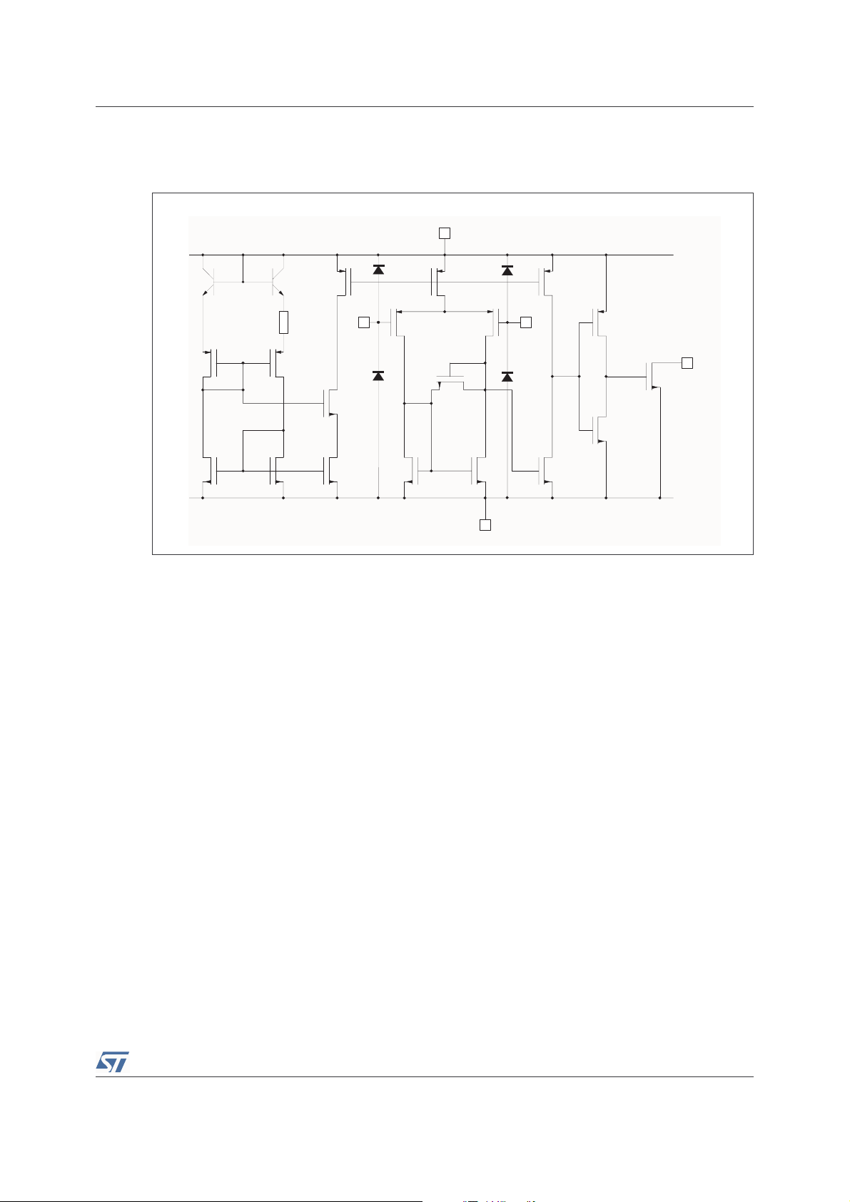
TS393 Typical Application Schematics
2 Typical Application Schematics
Figure 1. Schematic diagram (for 1/2 TS393)
V+
CC
T
T
1
T
2
T
9
10
T
17
R
1
Input - Input +
TT
34
T
8
T
5
T
T
6
7
T
11
TT
14 15
T
12
T
13
T
16
V-
CC
T
18
Output
T
20
T
19
3/9
 Loading...