

STMicroelectronics TS3702 Technical data
Micropower dual CMOS voltage comparators
1
2
3
45
6
7
8
Inverting Input 2
Output 2
Non-inverting Input 2
Output 1
Inverting Input 1
Non-inverting Input 1
CC
+
V
-
CC
V
-
+
-
+
Features
■ Push-pull CMOS output (no external pull-up
resistor required)
■ Extremely low supply current: 9μA typ /
comparator
■ Wide single supply range: 2.7V to 16V or dual
supplies (±1.35V to ±8V)
■ Extremely low input bias current: 1pA typ
■ Extremely low input offset currents: 1pA typ
■ Input common-mode voltage range includes
GND
■ High input impedance: 10
■ Fast response time: 2μs typ for 5mV overdrive
■ Pin-to-pin and functionally compatible with
bipolar LM393
Description
12
Ω typ
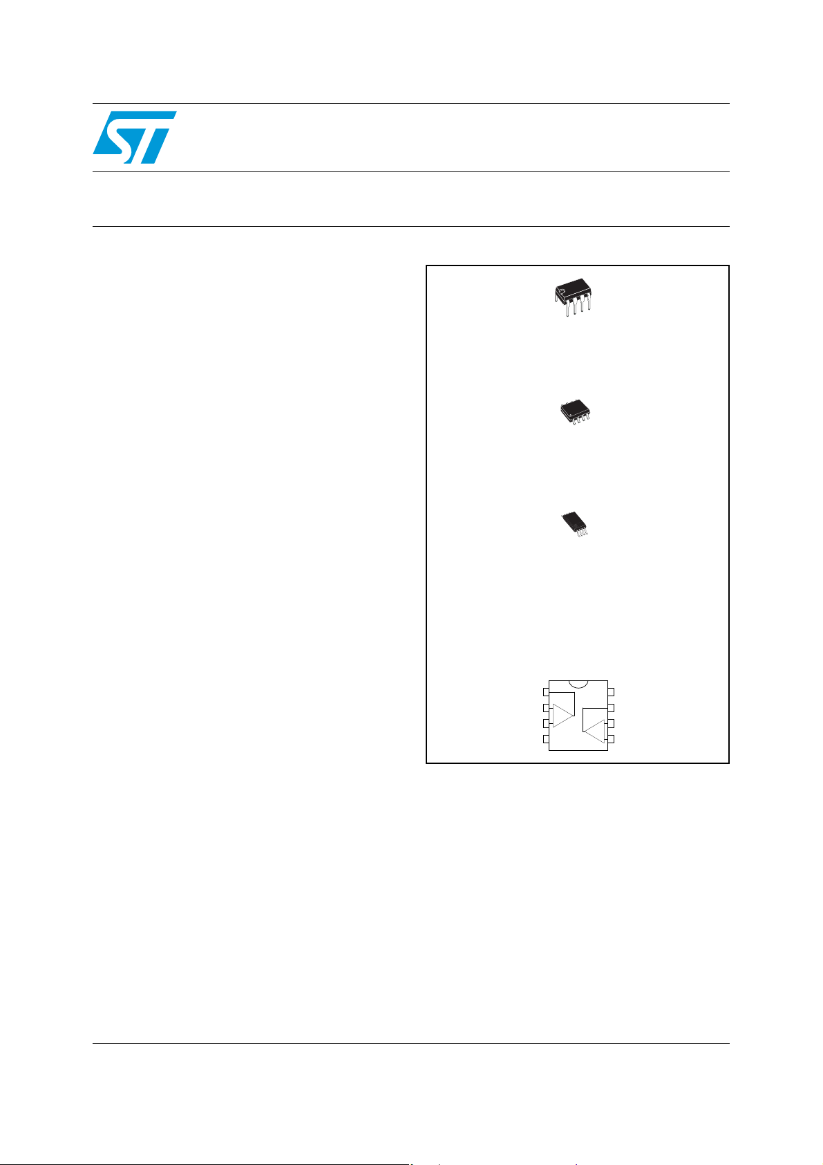
TS3702
N
DIP8
(Plastic package)
D
SO8
(Plastic micropackage)
P
TSSOP8
(Thin shrink small outline package)
The TS3702 is a micropower CMOS dual voltage
comparator with extremely low consumption of
9μA typ / comparator (20 times less than bipolar
LM393). The push-pull CMOS output stage allows
power and space saving by eliminating the
external pull-up resistor required by usual opencollector output comparators.
Thus response times remain similar to the LM393.
Pin connections
(Top view)
February 2007 Rev 3 1/11
www.st.com
11
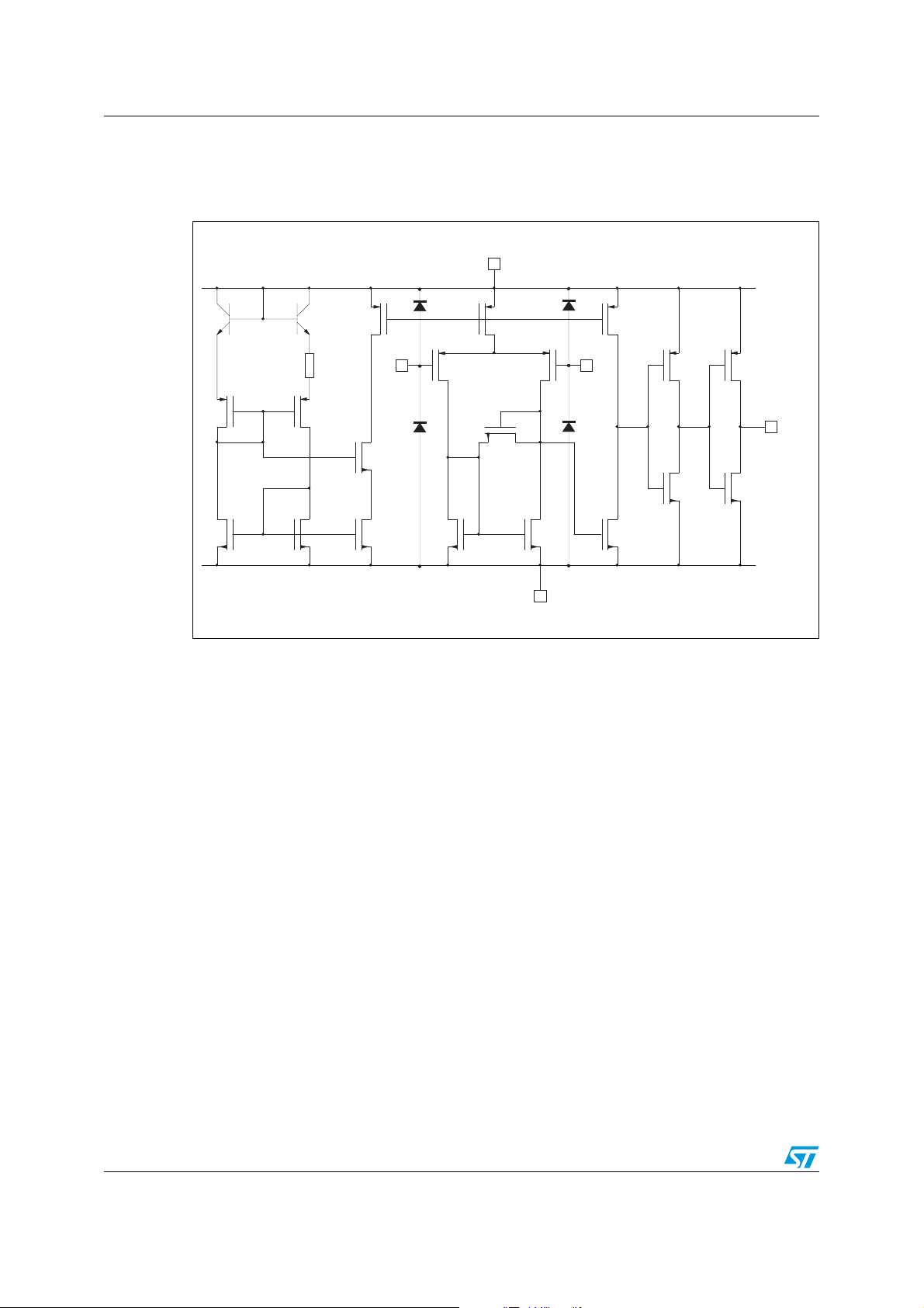
Schematic diagram TS3702
1 Schematic diagram
Figure 1. Schematic diagram (for 1/2 TS3702)
V+
CC
T
T
1
T
2
T
9
10
T
17
R
1
Input - Input +
TT
34
T
8
T
5
T
6
T
7
T
11
TT
14 15
T
12
T
13
T
16
V-
CC
TT
18 21
Output
TT
19 20
2/11
TS3702 Absolute maximum ratings and operating conditions
2 Absolute maximum ratings and operating conditions
Table 1. Absolute maximum ratings
Symbol Parameter Value Unit
V
CC
V
V
V
I
I
p
T
stg
ESD
+
Supply voltage
Differential input voltage
id
Input voltage
i
Output voltage 18 V
o
Output current 20 mA
o
Forward current in ESD protection diodes on input
F
Power dissipation
d
DIP8
SO8
TSSOP8
Storage temperature range -65 to +150 °C
HBM: human body model
MM: machine model
CDM: charged device model
(3)
(1)
(5)
(7)
(2)
(6)
(8)
(4)
18 V
±18 V
18 V
50 mA
1250
710
625
400 V
50 V
1.5 kV
mW
1. All voltage values, except differential voltage, are with respect to network ground terminal.
2. Differential voltages are the non-inverting input terminal with respect to the inverting input terminal.
3. The magnitude of the input and the output voltages must never exceed the magnitude of the positive and
negative supply voltages.
4. Guaranteed by design.
5. Pd is calculated with T
R
= 100°C/W for DIP8 package
thja
R
= 175°C/W for SO8 package
thja
R
= 200°C/W for TSSOP8 package
thja
6. Human body model: A 100pF capacitor is charged to the specified voltage, then discharged through a
1.5kΩ resistor between two pins of the device. This is done for all couples of connected pin combinations
while the other pins are floating.
7. Machine model: A 200pF capacitor is charged to the specified voltage, then discharged directly between
two pins of the device with no external series resistor (internal resistor < 5Ω). This is done for all couples of
connected pin combinations while the other pins are floating.
8. Charged device model: all pins and the package are charged together to the specified voltage and then
discharged directly to the ground through only one pin. This is done for all pins.
Table 2. Operating conditions
= +25°C, Tj = +150°C and
amb
Symbol Parameter Value Unit
Supply voltage
+
V
CC
V
icm
TS3702C, TS3702I
TS3702M
2.7 to 16
4 to 16
Common mode input voltage range 0 to V
+
-1.5 V
CC
Operating free-air temperature range
T
oper
TS3702C
TS3702I
TS3702M
0 to +70
-40 to +125
-55 to +125
V
°C
3/11
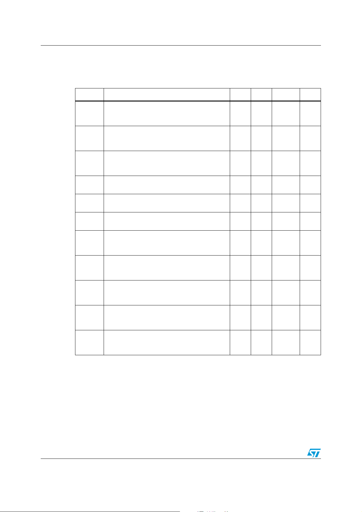
Electrical characteristics TS3702
3 Electrical characteristics
Table 3. V
CC
+
= 3V, V
-
= 0V, T
cc
= 25°C (unless otherwise specified)
amb
Symbol Parameter Min. Typ. Max. Unit
≤ T
≤ T
≤ T
≤ T
max
max
max
max
(2)
(2)
(1)
5
6.5
1
300
1
600
0
0
+
V
-1.2
CC
+
-1.5
V
CC
80 dB
V
io
I
io
I
ib
V
icm
CMR
SVR
Input offset voltage
Vic = 1.5V
T
≤ T
min
amb
Input offset current
Vic = 1.5V
≤ T
T
min
amb
Input bias current
Vic = 1.5V
T
≤ T
min
amb
Input common mode voltage range
≤ T
T
min
amb
Common-mode rejection ratio
Vic = V
icm min
Supply voltage rejection ratio
+
V
= 3V to 5V 75 dB
CC
High level output voltage
V
OH
V
= 1V, IOH = -4mA
id
≤ T
T
min
amb
≤ T
max
2
1.8
2.4
Low level output voltage
V
OL
= -1V, IOL = 4mA
V
id
T
≤ T
amb
≤ T
min
max
300 400
.
575
Supply current (each comparator)
I
CC
No load - Outputs low
≤ T
T
min
amb
≤ T
max
.
720
25
Response time low to high
t
PLH
Vic = 0V, f = 10kHz, CL = 50pF, overdrive = 5mV
TTL input
1.5
0.7
Response time high to low
t
PHL
1. The specified offset voltage is the maximun value required to drive the output up to 2.5V or down to 0.3V.
2. Maximum values include unavoidable inaccuracies of the industrial tests.
= 0V, f = 10kHz, CL = 50pF, overdrive = 5mV
V
ic
TTL input
2.2
0.15
mV
pA
pA
V
V
mV
μA
μs
μs
4/11
 Loading...