

Page 1
TS1871-TS1872-TS1874
1.8V Input/Output Rail-to-Rail
Low Power Operational Amplifiers
■ Operating at VCC = 1.8V to 6V
■ Rail-to-rail input & output
■ Extended Vicm (V
- 0.2V to VCC + 0.2V)
DD
■ Low supply current (400µA)
■ Gain bandwidth product (1.6MHz)
■ High stability
■ ESD tolerance (2kV)
■ Latch-up immunity
■ Available in SOT23-5 micropackage
Description
The TS187x (single, dual & quad) is an
operational amplifier family able to operate with
voltage as low as 1.8V and features both I/O railto-rail.
The common mode input voltage extends 200mV
at 25°C beyond the supply voltages while the
output voltage swing is within 100mV of each rail
with 600 Ohm load resistor. This device consumes
typically 400µA per channel while offering 1.6Mhz
of gain-bandwidth product. The amplifier provides
high output drive capability typically at 65mA-load.
These performances make the TS187X family
ideal for sensor interface, battery-supplied and
portable applications.
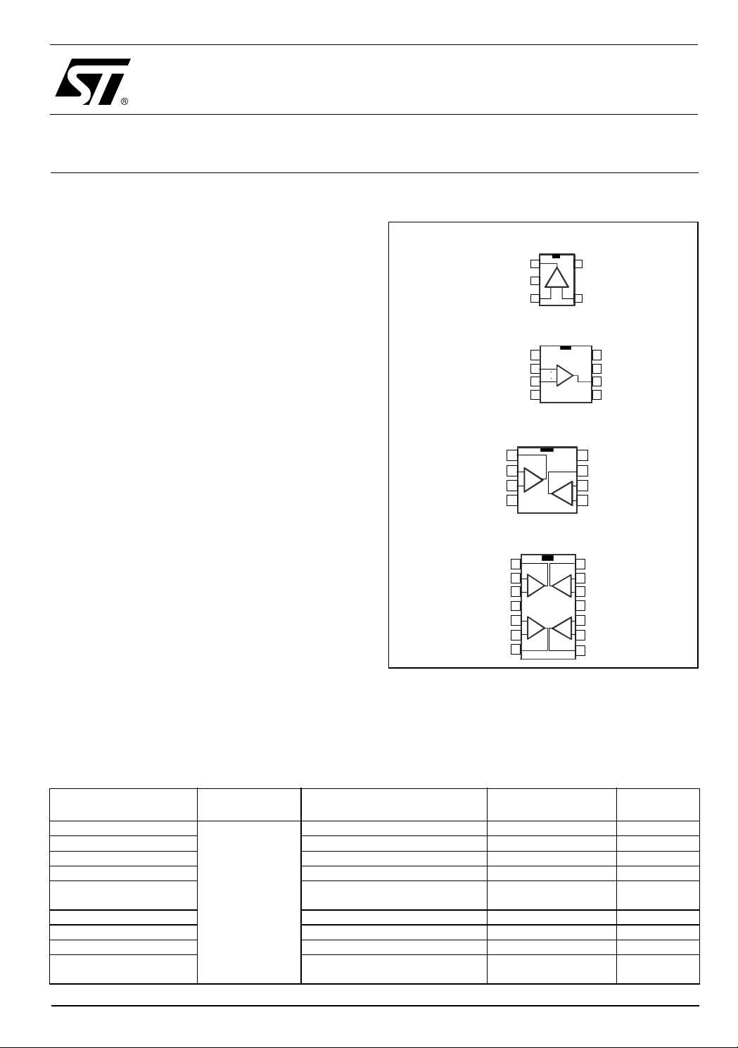
Pin Connections (top view)
TS1871ILT
VCC
Outp ut
Outp ut
1
1
VDD
VDD
2
2
Non Inverting I nput Inverting In put
Non Inverting I nput Inverting In put
3
3
TS1871ID-TS1871IDT
1
1
N.C.
N.C.
2
VDD
VDD
2
3
3
Inverting I nput
Inverting I nput
Non Inverting Input
Non Inverting Input
TS1872IST-TS1872IN-TS1872ID-TS1872IPT
Output 1
Output 1
1
1
_
Inverting Input 1
Inverting Input 1
Non Inverting Input 1
Non Inverting Input 1
VDD
VDD
_
2
2
+
+
3
3
TS1874IN-TS1874ID-TS1874IDT-TS1874IPT
1
1
Output 1
Output 1
Inverting Input 1
Inverting Input 1
Non Inverting Input 1
Non Inverting Input 1
Non Inverting Input 2
Non Inverting Input 2
Inverting Input 2
Inverting Input 2
Output 2
Output 2
VCC
VCC
_
_
2
2
+
+
3
3
5
5
+
+
_
_
6
6
7
7
5
5
4
4
_
_
+
+
_
_
+
+
14
14
_
_
13
13
+
+
12
12
114
114
10
10
+
+
_
_
9
9
8
8
VCC
8
8
7
7
6
6
54
54
8
8
VCC
VCC
7
7
Output 2
Output 2
6
6
Inverting Input 2
Inverting Input 2
Non Inverting Input 2
Non Inverting Input 2
54
54
Output 4
Output 4
Inverting Input 4
Inverting Input 4
Non Inverting Input 4
Non Inverting Input 4
VDD
VDD
Non Inverting Input 3
Non Inverting Input 3
Inverting Input 3
Inverting Input 3
Output 3
Output 3
N.C.
N.C.
VCC
VCC
Output
Output
N.C.
N.C.
Applications
■ Battery-powered applications (toys)
■ Portable communication devices (cell
phone)
■ Audio driver (headphone driver)
■ Laptop/notebook computers
Order Codes
Part Number
TS1871ID/IDT/AID/AIDT
TS1871ILT/AILT SOT23-5L Tape & Reel K171/K172
TS1872IN/AIN DIP Tube
TS1872ID/IDT/AID/AIDT SO Tube or Tape & Reel
TS1872IPT/AIPT TSSOP
TS1872IST/AIST mini SO Tape & Reel K171/K172
TS1874IN/AIN DIP Tube
TS1874ID/IDT/AID/AIDT SO Tube or Tape & Reel
TS1874IPT/AIPT TSSOP
May 2005 Revision 2 1/22
Temperature
Range
-40°C, +125°C
Package Packaging Marking
SO Tube or Tape & Reel
(Thin Shrink Outline Package)
(Thin Shrink Outline Package)
Tape & Reel
Tape & Reel
Page 2
TS1871-TS1872-TS1874 Absolute Maximum Ratings
1 Absolute Maximum Ratings
Table 1: Key parametes and their absolute maximum ratings
Symbol Parameter Value Unit
V
T
R
Supply voltage
CC
V
Differential Input Voltage
id
V
Input Voltage
i
Storage Temperature
stg
T
Maximum Junction Temperature
j
Thermal Resistance Junction to Ambient
thja
SOT23-5
SO8
SO14
TSSOP8
TSSOP14
miniSO8
HBM: Human Body Model
ESD
MM: Machine Model
CDM: Charged Device Model 1.5 kV
Latch-up Immunity 200 mA
Lead Temperature (soldering, 10sec) 250 °C
Output Short Circuit Duration
1) All voltages values, except differential voltage are with respect to network terminal.
2) Differential voltages are the non-inverting input terminal with respect to the inverting input terminal. If Vid > ±1V, the maximum input current must not exceed ±1mA. In this case (Vid > ±1V) an input serie resistor must be added to limit input current.
3) Short-circuits can cause excessive heating. Destructive dissipation can result from simultaneous short-circuit on all amplifiers
4) Human body model, 100pF discharged through a 1.5kΩ resistor into pin of device.
5) Machine model ESD, a 200pF cap is charged to the specified voltage, then discharged directly into the IC with no external series resistor
(internal resistor < 5
6) Short-circuits from the output to V
the magnitude of V
1
2
V
DD
3
4
5
Ω), into pin to pin of device.
can cause excessive heating. The maximum output current is approximately 80mA, independent of
. Destructive dissipation can result from simultaneous short-circuits on all amplifiers.
cc
cc
7V
±1 V
-0.3 to VCC +0.3
V
-65 to +150 °C
150 °C
250
°C/W
125
103
120
100
190
2kV
200 V
see note
6
Table 2: Operating conditions
Symbol Parameter Value Unit
VCC Supply Voltage 1.8 to 6 V
Vicm
Vicm
T
1) At 25°C, for 1.8 ≤ VCC ≤ 6V, V
2) In full temperature range, both Rails can be reached when VCC does not exceed 5.5V.
Common Mode Input Voltage Range
Common Mode Input Voltage Range
Operating Free Air Temperature Range
oper
is extended to VDD - 0.2V, VCC + 0.2V.
icm
1
2
2/22
VDD - 0.2 to VCC + 0.2
VDD to V
CC
-40 to + 125 °C
V
V
Page 3
Electrical Characteristics TS1871-TS1872-TS1874
2 Electrical Characteristics
Tab le 3: VCC = +1.8V, VDD = 0V, RL, CL connected to VCC/2, T
Symbol Parameter Min. Typ. Max. Unit
Input Offset Voltage
V
= V
= V
= V
= V
CC
CC
CC
/2
TS1871/2/4
TS1871A/2A/4A
1
/2
1)
/2
= V
CC
/2
= 0.5V to 1.3V
V
out
R
= 2kΩ
L
out
RL = 600Ω
icm
icm
icm
≤ V
= V
= V
icm
out
out
out
≤ VCC, V
V
io
∆V
I
io
I
ib
CMR
Input Offset Voltage Drift
io
Input Offset Current
V
Input Bias Current
V
Common Mode Rejection Ratio
0
SVR Supply Voltage Rejection Ratio 70 80 dB
Large Signal Voltage Gain
A
vd
= 25°C (unless otherwise specified)
amb
0.1 3
1
2
330nA
40 125 nA
55 77
77
70
92
85
mV
µV/°C
dB
dB
High Level Output Voltage
V
= 100mV
V
OH
id
R
= 2kΩ
L
RL = 600Ω
1.65
1.62
1.77
1.74
Low Level Output Voltage
= -100mV
V
V
OL
id
R
= 2kΩ
L
RL = 600Ω
88
115
100
150
mV
Output Source Current
V
I
o
I
CC
GBP
SR
φm
= 100mV, VO = V
ID
DD
Output Sink Current
V
= -100mV, VO = V
ID
CC
Supply Current (per amplifier), Vout = Vcc/2
A
= 1, no load
VCL
Gain Bandwidth Product
R
= 10kΩ, CL = 100pF, f = 100kHz
L
Slew Rate
R
= 10kΩ, CL = 100pF, AV = 1
L
Phase Margin
C
= 100pF
L
20
20
65
65
mA
400 560
0.9 1.6 MHz
0.38 0.54 V/
53 Degrees
en Input Voltage Noise 27 nV/
THD Total Harmonic Distortion 0.01 %
V
µA
µs
√Hz
1) Maximum values including unavoidable inaccuracies of the industrial test.
3/22
Page 4
TS1871-TS1872-TS1874 Electrical Characteristics
Table 4: VCC = +3V, VDD = 0V, RL, CL connected to VCC/2, T
= 25°C (unless otherwise specified)
amb
Symbol Parameter Min. Typ. Max. Unit
Input Offset Voltage
V
= V
= V
= V
= V
CC
CC
CC
/2
TS1871/2/4
TS1871A/2A/4A
1
/2
1)
/2
= V
CC
/2
out
60 80
0.1 3
1
2
µV/°C
330nA
4 125 nA
V
io
∆V
I
io
I
ib
CMR
icm
out
Input Offset Voltage Drift
io
Input Offset Current
V
= V
icm
out
Input Bias Current
V
= V
icm
out
Common Mode Rejection Ratio
0
≤ V
≤ VCC, V
icm
SVR Supply Voltage Rejection Ratio 70 85 dB
Large Signal Voltage Gain
V
= 0.5V to 2.5V
A
out
vd
R
= 2kΩ
L
RL = 600Ω
80
74
92
95
High Level Output Voltage
V
= 100mV
V
OH
id
R
= 2kΩ
L
RL = 600Ω
2.82
2.80
2.95
2.95
mV
dB
dB
V
Low Level Output Voltage
V
= -100mV
V
OL
id
R
= 2kΩ
L
RL = 600Ω
88
115
L120
160
Output Source Current
V
I
o
I
CC
GBP
SR
φm
= 100mV, VO = V
ID
DD
Output Sink Current
V
= -100mV, VO = V
ID
CC
Supply Current (per amplifier), Vout = Vcc/2
= 1, no load
A
VCL
Gain Bandwidth Product
R
= 10kΩ, CL = 100pF, f = 100kHz
L
Slew Rate
R
= 10kΩ, CL = 100pF, AV = 1
L
Phase Margin
C
= 100pF
L
20
20
80
80
450 650
11.7 MHz
0.42 0.6 V/
53 Degrees
en Input Voltage Noise 27 nV/
THD Total Harmonic Distortion 0.01 %
1) Maximum values including unavoidable inaccuracies of the industrial test.
mV
mA
µA
µs
√Hz
4/22
Page 5
Electrical Characteristics TS1871-TS1872-TS1874
Table 5: V
= +5V, VDD = 0V, CL & RL connected to VCC/2, T
CC
= 25°C (unless otherwise
amb
specified)
Symbol Parameter Min. Typ. Max. Unit
Input Offset Voltage
V
= V
= V
= V
= V
/2
CC
1
/2
CC
1)
/2
CC
different of V
out
CC
TS1871/2/4
TS1871A/2A/4A
/2
R
RL = 600Ω
R
RL = 600Ω
= 2kΩ
L
= 2kΩ
L
0.1 3
1
2
µV/°C
330nA
70 130 nA
65 85 dB
83
77
4.80
4.75
92
85
4.95
4.90
icm
icm
icm
≤ V
= V
= V
icm
out
out
out
≤ VCC, V
V
io
∆V
I
io
I
ib
CMR
Input Offset Voltage Drift
io
Input Offset Current
V
Input Bias Current
V
Common Mode Rejection Ratio
0
SVR Supply Voltage Rejection Ratio 70 90 dB
Large Signal Voltage Gain
V
= 1V to 4V
A
out
vd
High Level Output Voltage
V
= 100mV
V
OH
id
mV
dB
V
Low Level Output Voltage
V
= -100mV
V
OL
id
R
= 2kΩ
L
RL = 600Ω
88
115
130
188
Output Source Current
I
o
I
CC
GBP
SR
φm
V
ID
DD
Output Sink Current
V
= -100mV, VO = V
ID
CC
Supply Current (per amplifier), Vout = Vcc/2
A
= 1, no load
VCL
Gain Bandwidth Product
R
= 10kΩ, CL = 100pF, f = 100kHz
L
Slew Rate
R
= 10kΩ, CL = 100pF, AV = 1
L
Phase Margin
C
= 100pF
L
20
20
80
80
500 835
11.8 MHz
0.42 0.6 V/
55 Degrees
= 100mV, VO = V
en Input Voltage Noise 27 nV/
THD Total Harmonic Distortion 0.01 %
1) Maximum values including unavoidable inaccuracies of the industrial test.
mV
mA
µA
µs
√Hz
5/22
Page 6
TS1871-TS1872-TS1874 Electrical Characteristics
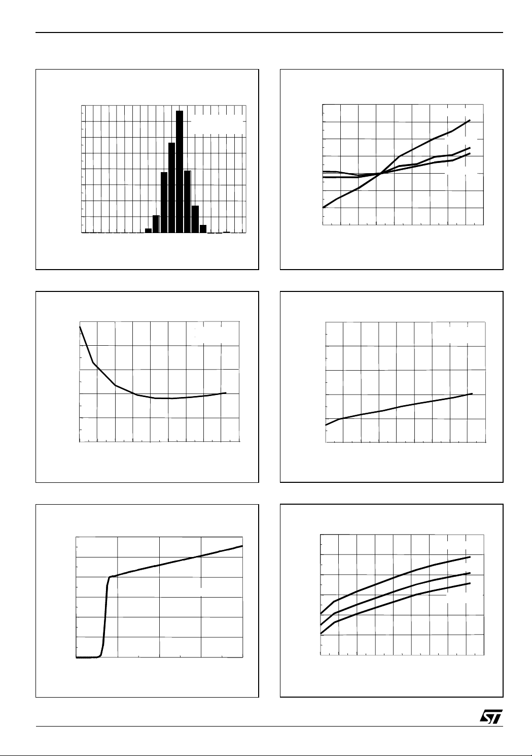
Figure 1 :
160
160
140
140
120
120
100
100
80
80
60
60
Quantity of pieces
Quantity of pieces
40
40
20
20
0
0
Figure 2 :
10.0
10.0
0.0
0.0
Input Offset Voltage Distribution
Input Offset Voltage Distribution
492 pieces tested
492 pieces tested
492 pieces tested
Vcc = 5V
Vcc = 5V
Vcc = 5V
Temp = +25°C
Temp = +25°C
Temp = +25°C
-2. -1.6 -1.2 -.8 -.4 0 .4 .8 1.2 1.6 2
-2. -1.6 -1.2 -.8 -.4 0 .4 .8 1.2 1.6 2
Input Offset Voltage (mV)
Input Offset Voltage (mV)
Input Bias Current vs. Temperature
Input Bias Current vs. Temperature
Vcc = 1.8V
Vcc = 1.8V
Vicm = 0.9V
Vicm = 0.9V
Figure 4 :
200
200
150
150
100
100
50
50
0
0
-50
-50
Input Voltage Drift (µV)
Input Voltage Drift (µV)
-100
-100
-150
-150
-40 -20 0 20 4 0 60 80 100 120 140
-40 -20 0 20 4 0 60 80 100 120 140
Figure 5 :
10.0
10.0
0.0
0.0
Input Offset Voltage Drift vs. Temperature
Input Offset Voltage Drift vs. Temperature
Vcc = 1.8V
Vcc = 1.8V
Vcc = 3V
Vcc = 3V
Vcc = 5V
Vcc = 5V
Tempe rature ( °C)
Tempe rature ( °C)
Input Bias Current vs. Temperature
Input Bias Current vs. Temperature
Vcc = 3V
Vcc = 3V
Vicm = 1.5V
Vicm = 1.5V
-10.0
-10.0
-20.0
-20.0
Input bias current (nA)
Input bias current (nA)
-30.0
-30.0
-40.0
-40.0
-40 -20 0 20 40 60 80 100 120 140
-40 -20 0 20 40 60 80 100 120 140
Figure 3 :
600
600
500
500
400
400
300
300
200
200
Supply Current (µA)
Supply Current (µA)
100
100
0
0
02468
02468
Temperature (°C)
Temperature (°C)
Supply Current / Amplifier vs. Supply Voltage
Supply Current / Amplifier vs. Supply Voltage
Tamb = 25°C
Tamb = 25°C
Supply Voltage (V)
Supply Voltage (V)
-10.0
-10.0
-20.0
-20.0
Input bias current (nA)
Input bias current (nA)
-30.0
-30.0
-40.0
-40.0
Figure 6 :
550
550
500
500
450
450
400
400
350
350
Supply Current (µA)
Supply Current (µA)
300
300
250
250
-40 -20 0 20 40 60 80 100 12 0 140
-40 -20 0 20 40 60 80 100 12 0 140
-40 -20 0 20 40 60 80 100 120 140
-40 -20 0 20 40 60 80 100 120 140
Supply Current / Amplifier vs. Temperature
Supply Current / Amplifier vs. Temperature
Temperature (°C)
Temperature (°C)
Temperature (°C)
Temperature (°C)
Vcc = 5V
Vcc = 5V
Vcc = 3V
Vcc = 3V
Vcc = 1.8V
Vcc = 1.8V
6/22
Page 7
Electrical Characteristics TS1871-TS1872-TS1874
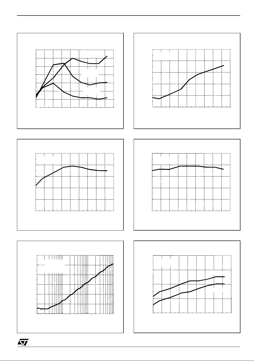
Figure 7 :
120
120
115
115
110
110
105
105
100
100
95
95
Common Mode Rejection (dB)
Common Mode Rejection (dB)
90
90
85
85
-40 -20 0 20 40 60 8 0 100 120 140
-40 -20 0 20 40 60 8 0 100 120 140
Figure 8 :
110
110
100
100
Common Mode Rejection vs. Temperature
Common Mode Rejection vs. Temperature
Vcc = 1.8V
Vcc = 1.8V
Vicm = 0V
Vicm = 0V
Vcc = 3V
Vcc = 3V
Vicm = 0V
Vicm = 0V
Vcc = 5V
Vcc = 5V
Vicm = 0V
Vicm = 0V
Temperature (°C)
Temperature (°C)
Supply Voltage Rejection vs. Temperature
Supply Voltage Rejection vs. Temperature
Vcc = 3V
Vcc = 3V
Vicm = 0V
Vicm = 0V
Figure 10 :
Supply Voltage Rejection vs. Temperature
Supply Voltage Rejection vs. Temperature
110
110
Vcc = 1.8V
Vcc = 1.8V
Vicm = 0V
Vicm = 0V
100
100
90
90
80
80
70
70
Supply Voltage Rejection (dB)
Supply Voltage Rejection (dB)
60
60
-40-200 2040 6080100120140
-40-200 2040 6080100120140
Figure 11 :
110
110
Vcc = 5V
Vcc = 5V
Vicm = 0V
Vicm = 0V
100
100
Temperature (°C)
Temperature (°C)
Supply Voltage Rejection vs. Temperature
Supply Voltage Rejection vs. Temperature
90
90
80
80
70
70
Supply Voltage Rejection (dB)
Supply Voltage Rejection (dB)
60
60
-40 -20 0 20 40 60 80 100 120 140
-40 -20 0 20 40 60 80 100 120 140
Temperature (°C)
Temperature (°C)
Figure 9 :
Power Supply Voltage Rejection vs. Frequency
Power Supply Voltage Rejection vs. Frequency
-20
-20
Vcc = 1.8V
Vcc = 1.8V
-30
-30
Vicm = 0.7V
Vicm = 0.7V
Gain = 10
Gain = 10
-40
-40
-50
-50
-60
-60
-70
-70
Supply Voltage Rejection (dB)
Supply Voltage Rejection (dB)
-80
-80
100 1000 10000 100000
100 1000 10000 100000
Frequency (H z)
Frequency (H z)
90
90
80
80
70
70
Supply V oltage Rejection (dB)
Supply V oltage Rejection (dB)
60
60
-40 -20 0 2 0 4 0 60 80 100 120 140
-40 -20 0 2 0 4 0 60 80 100 120 140
Figure 12 :
110
110
100
100
90
90
Open Loop Gain (dB)
Open Loop Gain (dB)
80
80
70
70
-40-200 20406080100120140
-40-200 20406080100120140
Temperatu re (°C)
Temperatu re (°C)
Open Loop Gain vs. Temperature
Open Loop Gain vs. Temperature
Vcc = 1.8V
Vcc = 1.8V
Vicm = 0.9V
Vicm = 0.9V
Temperature (°C)
Temperature (°C)
RL = 2 kOhms
RL = 2 kOhms
RL = 600 Ohm s
RL = 600 Ohm s
7/22
Page 8

TS1871-TS1872-TS1874 Electrical Characteristics
Figure 13 :
110
110
Vcc = 3V
Vcc = 3V
Vicm = 1.5V
Vicm = 1.5V
100
100
90
90
80
80
Open Loop Gain (dB)
Open Loop Gain (dB)
70
70
-40-200 20406080100120140
-40-200 20406080100120140
Figure 14 :
High Level Output Voltage vs. Temperature
High Level Output Voltage vs. Temperature
110
110
100
100
90
90
80
80
70
70
60
60
50
50
Voltage Reference d to VCC (mV)
Voltage Reference d to VCC (mV)
40
40
-40 -20 0 20 40 60 80 100 120 140
-40 -20 0 20 40 60 80 100 120 140
Open Loop Gain vs. Temperature
Open Loop Gain vs. Temperature
Tempe rature ( °C)
Tempe rature ( °C)
RL = 600 ohms
RL = 600 ohms
Vcc = 5V
Vcc = 5V
Vcc = 3V
Vcc = 3V
Vcc = 1.8V
Vcc = 1.8V
Temperature (°C)
Temperature (°C)
RL = 2 kOhms
RL = 2 kOhms
RL = 600 Oh ms
RL = 600 Oh ms
Figure 16 :
110
110
Vcc = 5V
Vcc = 5V
Vicm = 2.5V
Vicm = 2.5V
100
100
90
90
80
80
Open Loop Gain (dB)
Open Loop Gain (dB)
70
70
-40 -20 0 20 40 60 80 100 120 140
-40 -20 0 20 40 60 80 100 120 140
Figure 17 :
Low Level Output Voltage vs. Temperature
Low Level Output Voltage vs. Temperature
110
110
100
100
90
90
80
80
70
70
60
60
50
50
Voltage Ref erenced to Gnd (mV)
Voltage Ref erenced to Gnd (mV)
40
40
-40 -20 0 20 40 60 8 0 100 120 140
-40 -20 0 20 40 60 8 0 100 120 140
Open Loop Gain vs. Temperature
Open Loop Gain vs. Temperature
Temperature (°C)
Temperature (°C)
RL = 600 ohms
RL = 600 ohms
Temperature (°C)
Temperature (°C)
RL = 2 kOhms
RL = 2 kOhms
RL = 600 ohm s
RL = 600 ohm s
Vcc = 5V
Vcc = 5V
Vcc = 3V
Vcc = 3V
Vcc = 1.8V
Vcc = 1.8V
Figure 15 :
High Level Output Voltage vs. Temperature
High Level Output Voltage vs. Temperature
80
80
70
70
60
60
50
50
40
40
30
30
Voltage Referenced to VCC (mV)
Voltage Referenced to VCC (mV)
20
20
-40 -20 0 20 4 0 60 80 100 120 140
-40 -20 0 20 4 0 60 80 100 120 140
8/22
RL = 2 kohms
RL = 2 kohms
Temperature (°C)
Temperature (°C)
Vcc = 5V
Vcc = 5V
Vcc = 3V
Vcc = 3V
Vcc = 1.8V
Vcc = 1.8V
Figure 18 :
80
80
70
70
60
60
50
50
40
40
30
30
Voltage Referenced to Gnd (mV)
Voltage Referenced to Gnd (mV)
20
20
-40 -20 0 20 40 60 80 100 120 140
-40 -20 0 20 40 60 80 100 120 140
Low Level Output Voltage vs. Temperature
Low Level Output Voltage vs. Temperature
RL = 2 kohms
RL = 2 kohms
Vcc = 5V
Vcc = 5V
Vcc = 3V
Vcc = 3V
Vcc = 1.8V
Vcc = 1.8V
Temperature (°C)
Temperature (°C)
Page 9

Electrical Characteristics TS1871-TS1872-TS1874
Figure 19 :
100
100
50
50
0
0
Output Current (mA)
Output Current (mA)
-50
-50
-100
-100
-40 -20 0 20 40 60 80 100 120 140
-40 -20 0 20 40 60 80 100 120 140
Figure 20 :
100
100
50
50
0
0
Output Current (mA)
Output Current (mA)
-50
-50
-100
-100
-40 -20 0 20 40 60 80 100 120 140
-40 -20 0 20 40 60 80 100 120 140
Output Current vs. Temperature
Output Current vs. Temperature
Isink
Isink
Vcc = 1.8V
Vcc = 1.8V
Vid = 1V
Vid = 1V
Isource
Isource
Temperature (°C)
Temperature (°C)
Output Current vs. Temperature
Output Current vs. Temperature
Isink
Isink
Vcc = 5V
Vcc = 5V
Vid = 1V
Vid = 1V
Isource
Isource
Temperature (°C)
Temperature (°C)
Figure 22 :
100
100
50
50
0
0
Output Current (mA)
Output Current (mA)
-50
-50
-100
-100
-40 -20 0 20 40 60 80 100 120 140
-40 -20 0 20 40 60 80 100 120 140
Figure 23 :
100
100
50
50
0
0
Output Current (mA)
Output Current (mA)
-50
-50
-100
-100
0.00.51.01.52.0
0.00.51.01.52.0
Output Current vs. Temperature
Output Current vs. Temperature
Isink
Isink
Vcc = 3V
Vcc = 3V
Vid = 1V
Vid = 1V
Isource
Isource
Temperature (°C)
Temperature (°C)
Output Current vs. Temperature
Output Current vs. Temperature
T = 25 °C
T = -4 0 °C
T = -4 0 °C
T = -40 °C
T = -40 °C
T = 125 °C
T = 125 °C
T = 25 °C
T = 25 °C
T = 125 °C
T = 125 °C
Output Voltage (V)
Output Voltage (V)
T = 25 °C
Vcc = 1.8V
Vcc = 1.8V
Vid = 0.1V
Vid = 0.1V
Vicm = 0.9V
Vicm = 0.9V
sink
sink
source
source
Figure 21 :
100
100
50
50
0
0
Output Current (mA)
Output Current (mA)
-50
-50
-100
-100
0.0 0.5 1.0 1.5 2.0 2.5 3.0 3.5
0.0 0.5 1.0 1.5 2.0 2.5 3.0 3.5
Output Current vs. Temperature
Output Current vs. Temperature
T = -4 0 °C
T = -4 0 °C
T = 125 °C
T = 125 °C
Vcc = 3V
Vcc = 3V
Vid = 0.1V
Vid = 0.1V
Vicm = 1.5V
T = 125 °C
T = 125 °C
T = 25 ° C
T = 25 ° C
T = -40 °C
T = -40 °C
Vicm = 1.5V
Output Vol tage (V)
Output Vol tage (V)
sink
sink
T = 25 °C
T = 25 °C
source
source
Figure 24 :
100
100
50
50
0
0
Output Current (mA)
Output Current (mA)
-50
-50
-100
-100
0.0 1.0 2.0 3.0 4.0 5.0
0.0 1.0 2.0 3.0 4.0 5.0
Output Current vs. Temperature
Output Current vs. Temperature
T = -40 °C
T = -40 °C
sink
sink
T = 125 °C
T = 125 °C
Vcc = 5V
Vcc = 5V
Vid = 0.1V
Vid = 0.1V
Vicm = 2 .5V
T = 125 °C
T = 125 °C
T = 25 °C
T = 25 °C
T = -40 °C
T = -40 °C
Vicm = 2 .5V
Output Voltage (V)
Output Voltage (V)
T = 25 °C
T = 25 °C
source
source
9/22
Page 10

TS1871-TS1872-TS1874 Electrical Characteristics
Figure 25 :
70
70
60
60
50
50
40
40
gain
gain
Gain (dB)
Gain (dB)
30
30
20
20
10
10
0
0
1E+3 1E+4 1E+5 1E+6
1E+3 1E+4 1E+5 1E+6
Figure 26 :
70
70
60
60
50
50
40
40
gain
gain
Gain (dB)
Gain (dB)
30
30
20
20
10
10
0
0
1E+3 1E+4 1E+5 1E+6
1E+3 1E+4 1E+5 1E+6
Gain and Phase vs. Frequency
Gain and Phase vs. Frequency
RL = 10K
RL = 10K
CL = 100 pF
CL = 100 pF
Vcc = 1.8V
Vcc = 1.8V
phase
phase
Frequency (Hz)
Frequency (Hz)
Gain and Phase vs. Frequency
Gain and Phase vs. Frequency
RL = 10K
RL = 10K
CL = 100 pF
CL = 100 pF
Vcc = 5V
Vcc = 5V
phase
phase
Frequency (Hz)
Frequency (Hz)
180
180
160
160
140
140
120
120
100
100
80
80
60
60
40
40
180
180
160
160
140
140
120
120
100
100
80
80
60
60
40
40
Figure 28 :
Gain and Phase vs. Frequency
Gain and Phase vs. Frequency
70
70
RL = 10K
60
60
50
50
Phase (°)
Phase (°)
40
40
gain
gain
30
30
Gain (dB)
Gain (dB)
20
20
10
10
0
0
1E+3 1E+4 1E+5 1E+6
1E+3 1E+4 1E+5 1E+6
Frequency (Hz)
Frequency (Hz)
RL = 10K
CL = 100 pF
CL = 100 pF
Vcc = 3V
Vcc = 3V
phase
phase
180
180
160
160
140
140
120
120
100
100
80
80
60
60
40
40
Phase (°)
Phase (°)
Figure 29 :
Gain-Bandwidth Product vs. Temperature
Gain-Bandwidth Product vs. Temperature
1.70
1.70
1.60
1.60
Phase (°)
Phase (°)
1.50
1.50
1.40
1.40
1.30
1.30
Gain-Ba ndwidth Product (MHz )
Gain-Ba ndwidth Product (MHz )
1.20
1.20
Vcc = 5V Vicm = Vcc/2
Vcc = 5V Vicm = Vcc/2
Vcc = 3V
Vcc = 3V
Vcc = 1.8V
Vcc = 1.8V
-40 -20 0 20 40 60 80 100 120 140
-40 -20 0 20 40 60 80 100 120 140
Temperature (°C)
Temperature (°C)
RL = 10kohms
RL = 10kohms
CL = 100 pF
CL = 100 pF
Figure 27 :
Gain-Bandwidth Product vs. Supply Voltage
Gain-Bandwidth Product vs. Supply Voltage
2.0
2.0
1.5
1.5
1.0
1.0
Gain -Ban dwidt h Product (MH z)
Gain -Ban dwidt h Product (MH z)
0.5
0.5
12345
12345
10/22
RL = 2 kohms
RL = 2 kohms
CL = 220 pF
CL = 220 pF
Vicm = Vcc/2
Vicm = Vcc/2
T = 25°C
T = 25°C
Supply Voltage (V)
Supply Voltage (V)
Figure 30 :
0.55
0.55
0.50
0.50
0.45
0.45
0.40
0.40
Slew Rate (V/µs)
Slew Rate (V/µs)
0.35
0.35
0.30
0.30
-40 -20 0 20 40 60 80 100 120 140
-40 -20 0 20 40 60 80 100 120 140
Slew Rate vs. Temperature
Slew Rate vs. Temperature
Vcc = 1.8V
Vcc = 1.8V
gain = +1
gain = +1
Vin = 0. 4 to 1.4V
Vin = 0. 4 to 1.4V
RL = 10kohms
RL = 10kohms
CL = 100 pF
CL = 100 pF
negative Slew Rate
negative Slew Rate
Temperature (°C)
Temperature (°C)
positive Slew Rate
positive Slew Rate
Page 11

Electrical Characteristics TS1871-TS1872-TS1874
Figure 31 :
0.70
0.70
0.65
0.65
0.60
0.60
0.55
0.55
0.50
0.50
Slew Ra te (V/µs )
Slew Ra te (V/µs )
0.45
0.45
0.40
0.40
0.35
0.35
-40 -20 0 20 40 60 80 100 1 20 140
-40 -20 0 20 40 60 80 100 1 20 140
Figure 32 :
60
60
50
50
40
40
30
30
20
20
Phase Margin (°)
Phase Margin (°)
10
10
0
0
-10
-10
10 100 1000
10 100 1000
Slew Rate vs. Temperature
Slew Rate vs. Temperature
positive Slew Rate
Vcc = 3V
Vcc = 3V
gain = +1
gain = +1
Vin = 1 to 2V
Vin = 1 to 2V
RL = 10kohms
RL = 10kohms
CL = 100 pF
CL = 100 pF
Temperature (°C)
Temperature (°C)
Phase Margin vs. Load Capacitor
Phase Margin vs. Load Capacitor
Load Capaci tor (pF)
Load Capaci tor (pF)
positive Slew Rate
negative Slew Rate
negative Slew Rate
Vcc = 1.8V
Vcc = 1.8V
gain = 40dB
gain = 40dB
RL = 1Kohms
RL = 1Kohms
Figure 34 :
0.75
0.75
0.70
0.70
0.65
0.65
0.60
0.60
0.55
0.55
0.50
0.50
Slew Rate (V/µs)
Slew Rate (V/µs)
0.45
0.45
0.40
0.40
0.35
0.35
-40 -20 0 20 40 60 80 100 120 140
-40 -20 0 20 40 60 80 100 120 140
Figure 35 :
80
80
75
75
70
70
65
65
60
60
55
55
Phase Margin (°)
Phase Margin (°)
50
50
45
45
40
40
-10 -5 0 5 10
-10 -5 0 5 10
Slew Rate vs. Temperature
Slew Rate vs. Temperature
Vcc = 5V
Vcc = 5V
gain = +1
gain = +1
Vin = 2 to 3V
Vin = 2 to 3V
RL = 10kohms
RL = 10kohms
CL = 100 pF
CL = 100 pF
Phase Margin vs. Output Current
Phase Margin vs. Output Current
DC Output Current (mA)
DC Output Current (mA)
positive S lew Rate
positive S lew Rate
negative S lew R ate
negative S lew R ate
Temperature (°C)
Temperature (°C)
Vcc = 1. 8V
Vcc = 1. 8V
RL = 1 kOhms
RL = 1 kOhms
CL = 220 pF
CL = 220 pF
Figure 33 :
0
0
-5
-5
-10
-10
-15
-15
Gain Margin (dB)
Gain Margin (dB)
-20
-20
-25
-25
-10 -5 0 5 10
-10 -5 0 5 10
Gain Margin vs. Output Current
Gain Margin vs. Output Current
Vcc = 1. 8V
Vcc = 1. 8V
RL = 1 kOhms
RL = 1 kOhms
CL = 220 pF
CL = 220 pF
DC Outp ut Current (mA)
DC Outp ut Current (mA)
Figure 36 :
35
35
30
30
25
25
20
20
15
15
10
10
Equival ent Input Noise (nV/sqr(Hz))
Equival ent Input Noise (nV/sqr(Hz))
5
5
1E+1 1E+2 1E+3 1E+4 1E+5
1E+1 1E+2 1E+3 1E+4 1E+5
Equivalent Input Noise vs. Frequency
Equivalent Input Noise vs. Frequency
Vcc = 1.8V
Vcc = 1.8V
gain = 100
gain = 100
Rs = 100 ohms
Rs = 100 ohms
Frequency (Hz)
Frequency (Hz)
11/22
Page 12

TS1871-TS1872-TS1874 Electrical Characteristics
Figure 37 :
100.000
100.000
10.000
10.000
1.000
1.000
0.100
0.100
Distortion (%)
Distortion (%)
0.010
0.010
0.001
0.001
0.00 0.10 0.20 0.30 0.40 0.50 0.60 0.70 0080
0.00 0.10 0.20 0.30 0.40 0.50 0.60 0.70 0080
Figure 38 :
100.000
100.000
10.000
10.000
1.000
1.000
Distortion vs. Output Voltage
Distortion vs. Output Voltage
RL= 1Kohms
RL= 1Kohms
Gain = -1
Gain = -1
F = 1000 Hz
F = 1000 Hz
Vcc = 1.8V
Vcc = 1.8V
Output Voltage (VRMS)
Output Voltage (VRMS)
Distortion vs. Output Voltage
Distortion vs. Output Voltage
RL= 1Kohms
RL= 1Kohms
Gain = -1
Gain = -1
F = 1000 Hz
F = 1000 Hz
Vcc = 5V
Vcc = 5V
Figure 40 :
100.000
100.000
10.000
10.000
1.000
1.000
0.100
0.100
Distortion (% )
Distortion (% )
0.010
0.010
0.001
0.001
0.00 0.20 0.40 0.60 0.80 1.00 1.20
0.00 0.20 0.40 0.60 0.80 1.00 1.20
Figure 41 :
100.000
100.000
10.000
10.000
1.000
1.000
Distortion vs. Output Voltage
Distortion vs. Output Voltage
RL= 1Kohms
RL= 1Kohms
Gain = -1
Gain = -1
F = 1000 Hz
F = 1000 Hz
Vcc = 3V
Vcc = 3V
Output Voltage (VRMS)
Output Voltage (VRMS)
Distortion vs. Output Voltage
Distortion vs. Output Voltage
RL= 150 ohms
RL= 150 ohms
Gain = -1
Gain = -1
F = 1000 Hz
F = 1000 Hz
Vcc = 2.7V
Vcc = 2.7V
0.100
0.100
Distortion (% )
Distortion (% )
0.010
0.010
0.001
0.001
0.00 0.50 1.00 1.50 2.00
0.00 0.50 1.00 1.50 2.00
Figure 39 :
100.000
100.000
10.000
10.000
1.000
1.000
0.100
0.100
Distortion (%)
Distortion (%)
0.010
0.010
0.001
0.001
0.00 0.20 0.40 0. 60 0.80 1.00 1.20
0.00 0.20 0.40 0. 60 0.80 1.00 1.20
Output Voltage (VRMS)
Output Voltage (VRMS)
Distortion vs. Output Voltage
Distortion vs. Output Voltage
RL= 1500 o hms
RL= 1500 o hms
Gain = -1
Gain = -1
F = 1000 Hz
F = 1000 Hz
Vcc = 2.7V
Vcc = 2.7V
Output Voltage (VRMS)
Output Voltage (VRMS)
0.100
0.100
Distortion (% )
Distortion (% )
0.010
0.010
0.001
0.001
0.00 0.20 0.40 0.60 0.80 1.00 1.20
0.00 0.20 0.40 0.60 0.80 1.00 1.20
Figure 42 :
100.000
100.000
10.000
10.000
1.000
1.000
0.100
0.100
Distortio n (%)
Distortio n (%)
0.010
0.010
0.001
0.001
0.00 0.20 0.,40 0.60 0.80 1.00 1.20
0.00 0.20 0.,40 0.60 0.80 1.00 1.20
Output Voltage (VRMS)
Output Voltage (VRMS)
Distortion vs. Output Voltage
Distortion vs. Output Voltage
RL= 4700 ohms
RL= 4700 ohms
Gain = -1
Gain = -1
F = 1000 Hz
F = 1000 Hz
Vcc = 2.7V
Vcc = 2.7V
Output Voltage (VRMS)
Output Voltage (VRMS)
12/22
Page 13

Electrical Characteristics TS1871-TS1872-TS1874
Figure 43 :
0.014
0.014
0.012
0.012
0.010
0.010
0.008
0.008
Distortion (%)
Distortion (%)
0.006
0.006
0,004.
0,004.
1E+1 1E+2 1E+3 1E+4 1E+5
1E+1 1E+2 1E+3 1E+4 1E+5
Figure 44 :
0.150
0.150
0.125
0.125
0.100
0.100
Distortion vs. Frequency
Distortion vs. Frequency
Vcc = 1.8V
Vcc = 1.8V
Vout = 1Vpp
Vout = 1Vpp
RL = 1Kohms
RL = 1Kohms
gain = -1
gain = -1
Frequency (Hz)
Frequency (Hz)
Distortion vs. Frequency
Distortion vs. Frequency
Vcc = 1.8V
Vcc = 1.8V
Vout = 1V pp
Vout = 1V pp
RL = 32 ohms
RL = 32 ohms
gain = -1
gain = -1
Figure 46 :
0.015
0.015
0.013
0.013
0.010
0.010
0.007
0.007
Distortion (%)
Distortion (%)
0.005
0.005
0.003
0.003
0.000
0.000
1E+1 1E+2 1E+3 1E+4 1E+5
1E+1 1E+2 1E+3 1E+4 1E+5
Figure 47 :
0.150
0.150
0.125
0.125
0.100
0.100
Distortion vs. Frequency
Distortion vs. Frequency
Vcc = 3V
Vcc = 3V
Vout = 1Vpp
Vout = 1Vpp
RL = 1Kohms
RL = 1Kohms
gain = -1
gain = -1
Freque ncy (Hz )
Freque ncy (Hz )
Distortion vs. Frequency
Distortion vs. Frequency
Vcc = 3V
Vcc = 3V
Vout = 1Vpp
Vout = 1Vpp
RL = 32 ohms
RL = 32 ohms
gain = -1
gain = -1
0.075
0.075
0.050
0.050
Distortion (%)
Distortion (%)
0.025
0.025
0.000
0.000
1E+1 1E+2 1E+3 1E+4 1E+5
1E+1 1E+2 1E+3 1E+4 1E+5
Figure 45 :
60
60
RL = 32 ohms
RL = 32 ohms
50
50
40
40
30
30
20
20
Output Power (mW)
Output Power (mW)
10
10
0
0
123456
123456
Freque ncy (H z)
Freque ncy (H z)
Output Power vs. Supply Voltage
Output Power vs. Supply Voltage
10% distor tion
10% distor tion
1% distortion
1% distortion
0.1% distortion
0.1% distortion
Supply Voltage (V)
Supply Voltage (V)
0.075
0.075
Distortion (%)
Distortion (%)
0.050
0.050
0.025
0.025
0.000
0.000
1E+1 1E+2 1E +3 1E+4 1E+5
1E+1 1E+2 1E +3 1E+4 1E+5
Frequency (Hz)
Frequency (Hz)
13/22
Page 14

TS1871-TS1872-TS1874 Package Mechanical Data
3 Package Mechanical Data
3.1 DIP8 package
Plastic DIP-8 MECHANICAL DATA
DIM.
A 3.3 0.130
a1 0.7 0.028
B 1.39 1.65 0.055 0.065
B1 0.91 1.04 0.036 0.041
b 0.5 0.020
b1 0.38 0.5 0.015 0.020
D 9.8 0.386
E 8.8 0.346
e 2.54 0.100
e3 7.62 0.300
e4 7.62 0.300
F 7.1 0.280
I 4.8 0.189
L 3.3 0.130
Z 0.44 1.6 0.017 0.063
MIN. TYP MAX. MIN. TYP. MAX.
mm. inch
14/22
P001F
Page 15

Package Mechanical Data TS1871-TS1872-TS1874
3.2 SO8 package
SO-8 MECHANICAL DATA
DIM.
A 1.35 1.75 0.053 0.069
A1 0. 10 0.25 0. 04 0.010
A2 1. 10 1.65 0. 043 0.065
B 0.33 0.51 0.013 0.020
C 0.19 0.25 0. 007 0.010
D 4.80 5.00 0. 189 0.197
E 3.80 4.00 0.150 0.157
e 1.27 0.050
H 5.80 6.20 0. 228 0.244
h 0.25 0.50 0.010 0.020
L 0.40 1.27 0.016 0.050
k ˚ (max.)
ddd 0.1 0.04
MIN. TYP MAX. MIN. TYP. MAX.
mm. inch
8
0016023/C
15/22
Page 16

TS1871-TS1872-TS1874 Package Mechanical Data
3.3 TSSOP8 package
TSSOP8 MECHANICAL DATA
DIM.
MIN. TYP MAX. MIN. TYP. MAX.
A 1.2 0.047
A1 0.05 0.15 0.002 0.006
A2 0.80 1.00 1.05 0.031 0.039 0.041
b 0.19 0.30 0.007 0.012
c 0.09 0.20 0.004 0.008
D 2.90 3.00 3.10 0.114 0.118 0.122
E 6.20 6.40 6.60 0.244 0.252 0.260
E1 4.30 4.40 4.50 0.169 0.173 0.177
e 0.65 0.0256
K0˚ 8˚0˚ 8˚
L 0.45 0.60 0.75 0.018 0.024 0.03 0
L1 1 0.039
mm. inch
16/22
0079397/D
Page 17

Package Mechanical Data TS1871-TS1872-TS1874
3.4 Mini SO8 package
17/22
Page 18

TS1871-TS1872-TS1874 Package Mechanical Data
3.5 DIP14 package
Plastic DIP-14 MECHANICAL DATA
DIM.
a1 0.51 0.020
B 1.39 1.65 0.055 0.065
b 0.5 0.020
b1 0.25 0.010
D 20 0.787
E 8.5 0.335
e 2.54 0.100
e3 15.24 0.600
F 7.1 0.280
I 5.1 0.201
L 3.3 0.130
Z 1.27 2.54 0.050 0.100
MIN. TYP MAX. MIN. TYP. MAX.
mm. inch
18/22
P001A
Page 19

Package Mechanical Data TS1871-TS1872-TS1874
3.6 SO14 package
SO-14 MECHANICAL DATA
DIM.
A 1.75 0.068
a1 0.1 0.2 0.003 0.007
a2 1.65 0.064
b 0.35 0.46 0.013 0.018
b1 0.19 0.25 0.007 0.010
C 0.5 0.019
c1 45˚ (typ.)
D 8.55 8.75 0. 336 0.344
E 5.8 6. 2 0.228 0. 244
e 1.27 0.050
e3 7.62 0.300
F 3.8 4.0 0.149 0.157
G 4.6 5.3 0.181 0. 208
L 0.5 1.27 0.019 0.050
M 0.68 0.026
S˚ (max.)
MIN. TYP MAX. MIN. TYP. MAX.
mm. inch
8
PO13G
19/22
Page 20

TS1871-TS1872-TS1874 Package Mechanical Data
3.7 TSSOP14 package
TSSOP14 MECHANICAL DATA
DIM.
A 1.2 0.047
A1 0.05 0.15 0.002 0.004 0.006
A2 0.8 1 1.05 0.031 0.039 0.041
b 0.19 0.30 0. 007 0.012
c 0.09 0.20 0.004 0.0089
D 4.9 5 5.1 0.193 0.197 0.201
E 6.2 6.4 6.6 0.244 0.252 0.260
E1 4.3 4.4 4.48 0.169 0.173 0.176
e 0.65 BSC 0.0256 BSC
K0˚ 8˚0˚ 8˚
L 0.45 0.60 0.75 0.018 0.024 0.030
A
MIN. TYP MAX. MIN. TYP. MAX.
A2
b
A1
mm. inch
e
D
c
K
L
E
20/22
PIN 1 IDENTIFICATION
E1
1
0080337D
Page 21

Package Mechanical Data TS1871-TS1872-TS1874
3.8 SOT23-5 package
SOT23-5L MECHANICAL DATA
DIM.
A 0.90 1.45 35.4 57.1
A1 0.00 0.15 0.0 5.9
A2 0.90 1.30 35.4 51.2
b 0.35 0.50 13.7 19.7
C 0.09 0.20 3.5 7.8
D 2.80 3.00 110.2 118.1
E 2.60 3.00 102.3 118.1
E1 1.50 1.75 59.0 68.8
e.95 37.4
e1 1.9 74.8
L 0.35 0.55 13.7 21.6
MIN. TYP MAX. MIN. TYP. MAX.
mm. mils
0
21/22
Page 22

TS1871-TS1872-TS1874 Revision History
4 Revision History
Date Revision Description of Changes
01 April 2002 1 First Release
01 Jan. 2005 2 Modifications on AMR Table 1 on page 2 (explanation of Vid and Vi limits)
Information furnished is believed to be accurate and reliable. However, STMicroelectronics assumes no responsibility for the consequences
of use of such information nor for any infringement of patents or other rights of third parties which may result from its use. No license is granted
by implication or otherwise under any patent or patent rights of STMicroelectronics. Specifications mentioned in this publication are subject
to change without notice. This publication supersedes and replaces all information previously supplied. STMicroelectronics products are not
authorized for use as critical components in life support devices or systems without express written approval of STMicroelectronics.
The ST logo is a registered trademark of STMicroelectronics
All other names are the property of their respective owners
© 2005 STMicroelectronics - All rights reserved
Australia - Belgium - Brazil - Canada - China - Czech Republic - Finland - France - Germany - Hong Kong - India - Israel - Italy - Japan -
Malaysia - Malta - Morocco - Singapore - Spa in - Sweden - Switzerland - United Kingdom - United States of America
STMicroelectronics group of companies
www.st.com
22/22
 Loading...