

Page 1
®
TPN3021
Application Specific Discretes
TRIPOLAR OVERVOLTAGE PROTECTION
A.S.D.™
FEATURES
Triple crowbar protection
■
Low capacitance
■
Low holding current: IH= 30mA minimum
■
Surge current: IPP= 200A, 2/10µs
■
= 30A, 10/1000µs
I
PP
MAIN APPLICATIONS
Dedicated to dataline protection, this device provides a tripolar protection function. It ensures the
same protection capability with the same breakdown voltage in both common and differential
modes.
DESCRIPTION
The TPN3021 is a low capacitance transient
surge arrestor designed for protection of high
debit rate communication network. Its low capacitance avoids distorsion of the signal as it
has been designed for T1/E1 and Ethernet networks.
FOR NETWORK INTERFACES
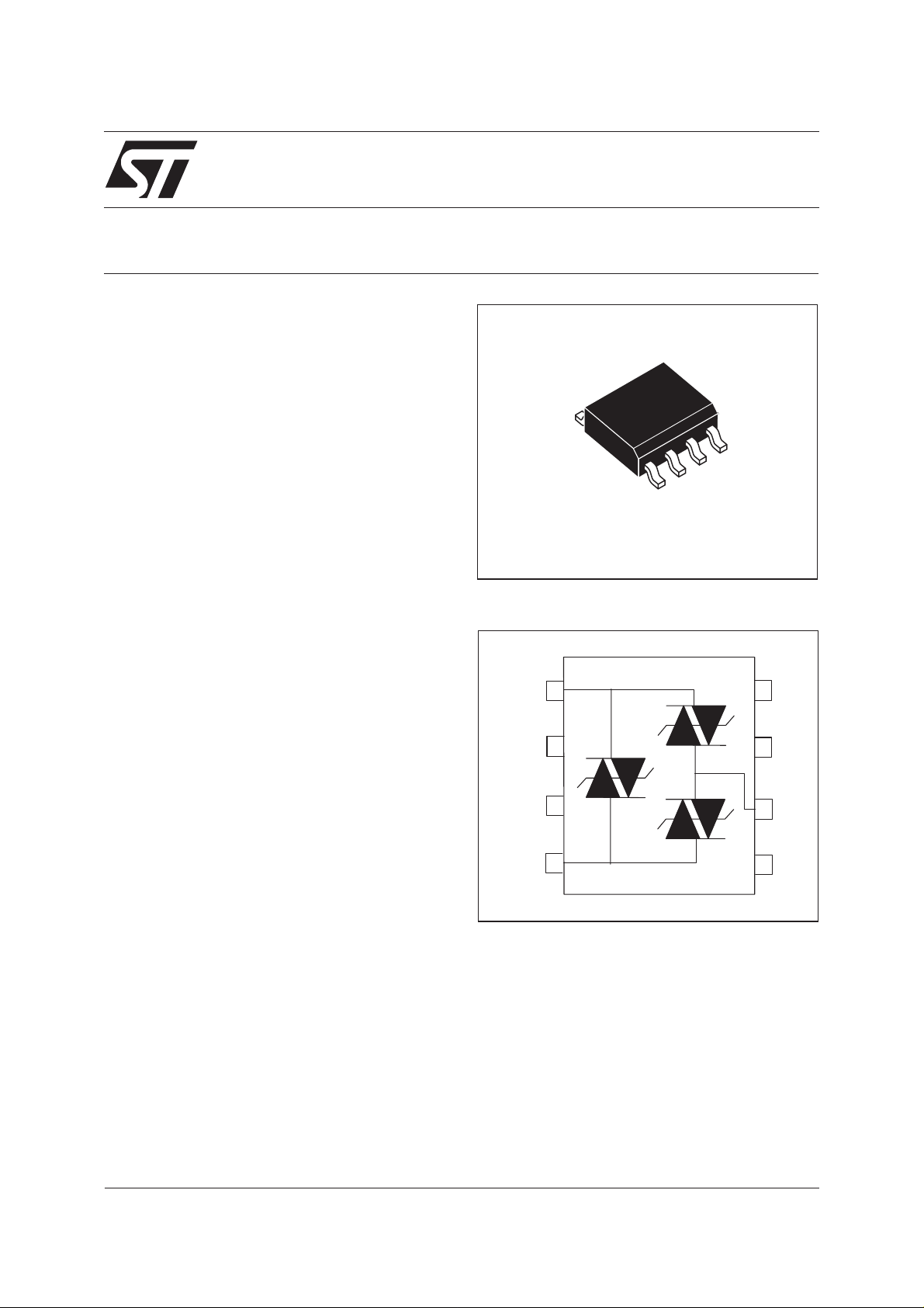
SO-8
SCHEMATIC DIAGRAM
Rx+ / Tx+
1
8
NC
BENEFITS
Trisil technology is not subject to ageing and provides a fail safe mode in short circuit for a better
protection. They are used to help equipment to
meet main standards such as UL1950, IEC950 /
CSA C22.2 and UL1459. Theyhave UL94 V0 approved resin. SO8 package is JEDEC registered.
Trisils comply with the following standards
GR-1089 Core, ITU-T-K20/K21, VDE0433,
VDE0878, IEC61000-4-2.
TM: ASDisa trademark of STMicroelectronics.
NC
NC
Rx- / Tx-
NC
2
3
4
7
GND
6
NC
5
September 2001 - Ed : 3
1/6
Page 2
TPN3021
IN COMPLIANCES WITH THE FOLLOWING STANDARDS
Standard
Peak surge
voltage (V)
Voltage
waveform
Required peak
current (A)
Current
waveform
Minimum se-
rial resistor to
meet standard
)
(
GR-1089 Core
First level
GR-1089 Core
2500
1000
1500 2/10 µs 100 2/10 µs 0
Intrabuilding
ITU-T-K20/K21
ITU-T-K20
(IEC61000-4-2)
VDE0433
VDE0878
IEC61000-4-5
1000 10/700 µs 25 5/310 µs 0
6000
8000
4000
2000
4000
2000
2000
2000
ELECTRICAL CHARACTERISTICS (T
Symbol Parameter
V
RM
V
BO
V
BR
I
H
I
BO
I
RM
I
PP
C
Stand-off voltage
Breakover voltage
Breakdown voltage
Holding current
Breakover current
Leakage current at V
Peak pulse current
Capacitance
RM
2/10 µs
10/1000 µs
500
100
1/60 ns ESD contact discharge
ESD air discharge
10/700 µs 100
50
1.2/50 µs 100
50
amb
=25°C)
10/700 µs
1.2/50 µs
50
50
2/10 µs
10/1000 µs
5/310 µs 40
1/20 µs 0
5/310 µs
8/20 µs
I
I
PP
I
BO
I
I
H
R
I
RM
V
RM
7.5
25
-
-
0
0
0
0
V
V
V
BR
V
BO
R
2/6
V
R
I
R
Continous reverse voltage
Leakage current at V
R
Page 3
TPN3021
ABSOLUTE RATINGS (T
amb
=25°C)
Symbol Parameter Value Unit
I
I
TSM
pp
Peak pulse pulse current: tr / tp
Non repetitive surge peak on-state current
One cycle
Non repetitive surge peak on-state current
F=50Hz
T
stg
Tj
T
L
Storage temperature range
Maximum junction temperature
Maximum lead temperature for soldering during 10s
Repetitive peak pulse current
10/1000 µs
8/20 µs
10/560 µs
5/310 µs
10/160 µs
1/20 µs
2/10 µs
50 Hz
60 Hz
0.2 s
%I
PP
100
2s
30
100
40
50
75
100
200
8
9
3
1.5
-55to+150
150
260 °C
tr: rise time (µs)
tp: pulse duration time (µs)
50
A
A
A
°C
°C
ex: pulse waveform
10/1000 µs tr = 10 µs tp = 1000 µs
0
t
t
p
r
t
THERMAL RESISTANCES
Symbol Parameter Value Unit
R
th(j-a)
Junction to ambient
ELECTRICAL PARAMETERS (T
Type IRM@V
max.
amb
RM
= 25°C)
V
max
max@I
BO
note 1
BO
note 2
170 °C/W
I
H
min.
note 3
typ.
µA V V mA mA pF
TPN3021 4 28 38 300 30 16
Note 1 : See test circuit 1
Note 2 : See functional holding current test circuit 2
Note 3 : VR= 0V bias, V
= 1V, F = 1MHz
RMS
C
3/6
Page 4

TPN3021
TEST CIRCUIT 1 FOR IBOAND VBOPARAMETERS
K
ton = 20ms
Vout
1/4
TEST PROCEDURE :
Pulse test duration (tp = 20ms):
- For bidirectional devices = switch K is closed
- For unidirectional devices = switch K is open
Vout selection
- Devices with Vbo < 200V: Vout = 250VRMS, R1 = 140Ω
- Devices with Vbo > 200V: Vout = 480VRMS, R2 = 240Ω
R1 = 140Ω
R2 = 240Ω
DUT
IBO
measurement
VBO
measurement
TEST CIRCUIT 2 FOR IHPARAMETER
R
Vbat < Vbr
Thisisa GO-NOGO testwhich allows toconfirmthe holding current(I
Test procedure:
1- Adjust the current level at the I
2- Fire the DUT with a surge current I
3- DUT must come back in off state within maximum 50ns.
value by short circuiting the DUT.
H
= 10A, 10/1000 µs.
PP
D.U.T
Surge generator
)levelin a functionaltestcircuit.
H
4/6
Page 5

TPN3021
Fig. 1: Non repetitive surge peak on-state current
versus overload duration (
ITSM(A)
12
10
8
6
4
2
0
1E-2 1E-1 1E+0 1E+1 1E+2 1E+3
t(s)
Tj initial = 25°C)
F=50Hz
Fig. 3: Relative variation of holding current versus
junction temperature.
IH[Tj] / IH[Tj=25°C]
1.8
1.6
1.4
1.2
1.0
0.8
0.6
0.4
0.2
0.0
-40 -20 0 20 40 60 80 100 120
Tj(°C)
Fig. 2: Variation of junction capacitanceversus re-
verse voltage applied (typical values).
C(pF)
22
20
18
16
14
12
10
8
6
4
2
0
0 5 10 15 20 25 30
VR(V)
Tj=25°C
F=1MHz
VRMS=1V
ORDER CODE
Tripolar
Protection
for Network
Numerical code
TPN 30 2 1 RL
Packaging:
RL = Tape & reel
= Tube
Package:
1 = SO-8 Plastic
Version
5/6
Page 6

TPN3021
PACKAGE MECHANICAL DATA
SO-8 (Plastic)
DIMENSIONS
REF.
Millimetres Inches
Min. Typ. Max. Min. Typ. Max.
A 1.75 0.069
a1 0.1 0.25 0.004 0.010
a2 1.65 0.065
b 0.35 0.48 0.014 0.019
b1 0.19 0.25 0.007 0.010
C 0.50 0.020
c1 45° (typ)
D 4.8 5.0 0.189 0.197
E 5.8 6.2 0.228 0.244
e 1.27 0.050
e3 3.81 0.150
F 3.8 4.0 0.15 0.157
L 0.4 1.27 0.016 0.050
M 0.6 0.024
S 8° (max)
Ordering code Marking Package Weight Base qty Delivery mode
TPN3021 TPN302 SO-8 0.08g 100 Tube
TPN3021RL TPN302 2500 Tape & reel
Informationfurnished is believedto be accurate andreliable. However, STMicroelectronicsassumes no responsibility forthe consequences of
useof such informationnor for anyinfringement of patentsor other rights ofthird parties whichmay result fromits use. Nolicenseis granted by
implication or otherwise under any patent or patent rights of STMicroelectronics. Specifications mentioned in this publication are subject to
change without notice. This publication supersedes and replaces all information previously supplied.
STMicroelectronics products are not authorized for use as critical components in life support devices or systems without express written
approval of STMicroelectronics.
The ST logo is a registered trademark of STMicroelectronics
© 2001 STMicroelectronics - Printed in Italy - All rights reserved.
STMicroelectronics GROUP OF COMPANIES
Australia - Brazil - China - Finland - France - Germany - Hong Kong - India - Italy - Japan - Malaysia
Malta - Morocco - Singapore - Spain - Sweden - Switzerland - United Kingdom - U.S.A.
http://www.st.com
6/6
Page 7

This datasheet has been download from:
www.datasheetcatalog.com
Datasheets for electronics components.
 Loading...