

Page 1
TPI8011N
ApplicationSpecific Discretes
A.S.D.
FEATURES
BIDIRECTIONALTRIPLE CROWBAR
PROTECTION.
PEAKPULSECURRENT:
I
=30A , 10/1000 µs.
PP
BREAKDOWN VOLTAGE:
TPI80xxN: 80V
TPI120xxN: 120V.
AVAILABLEIN SO8 PACKAGES.
LOWDYNAMICBREAKOVER VOLTAGE:
TPI80N: 150V
TPI120:200V
DESCRIPTION
Dedicateddevices forISDNinterfaceand high
speeddatatelecomline protection.Equivalentto
a triple TRISILwithlow capacitance.
Thesedevices provide:
low capacitance from lines to ground, allowing
-
high speed transmission without signal
attenuation.
- good capacitance balance between lines in
ordertoensurelongitudinalbalance.
- fixed breakdown voltage in both common and
differentialmodes.
- the same surge current capability in both
commonand differentialmodes.
A particular attention has been given to the
-
internalwirebonding.The”4-point”configuration
ensures a reliable protection, eliminating
overvoltages introduced by the parasitic
inductances of the wiring (Ldi/dt), especially for
veryfasttransientovervoltages.
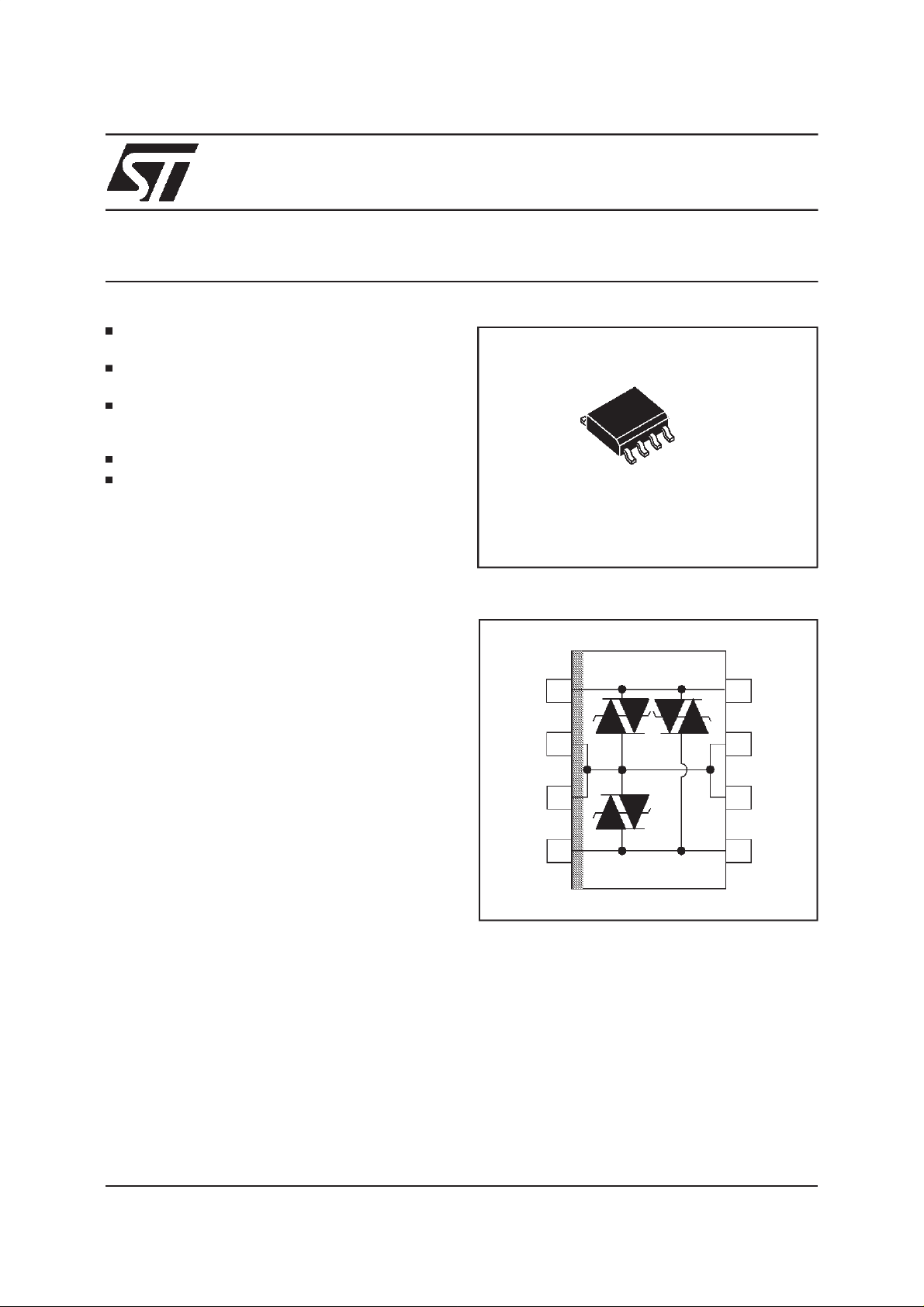
TPI12011N
TRIPOLAR PROTECTION
FOR ISDN INTERFACES
SO8
SCHEMATIC DIAGRAM
Tip
GND
GND
Ring
1
2
3
4
8
Tip
GND
7
GND
6
5
Ring
COMPLIESWITHTHEFOLLOWINGSTANDARDS:
CCITTK17 -K20 10/700 µs 1.5 kV
5/310µs38A
VDE0433 10/700 µs2kV
5/310µs50A
VDE0878 1.2/50µs 1.5 kV
1/20 µs40A
CNET 0.5/700µs 1.5 kV
0.2/310µs38A
TM: ASD is atrademark of SGS-THOMSONMicroelectronics.
November 1999 Ed : 3A
1/7
Page 2
TPI8011N/TPI12011N
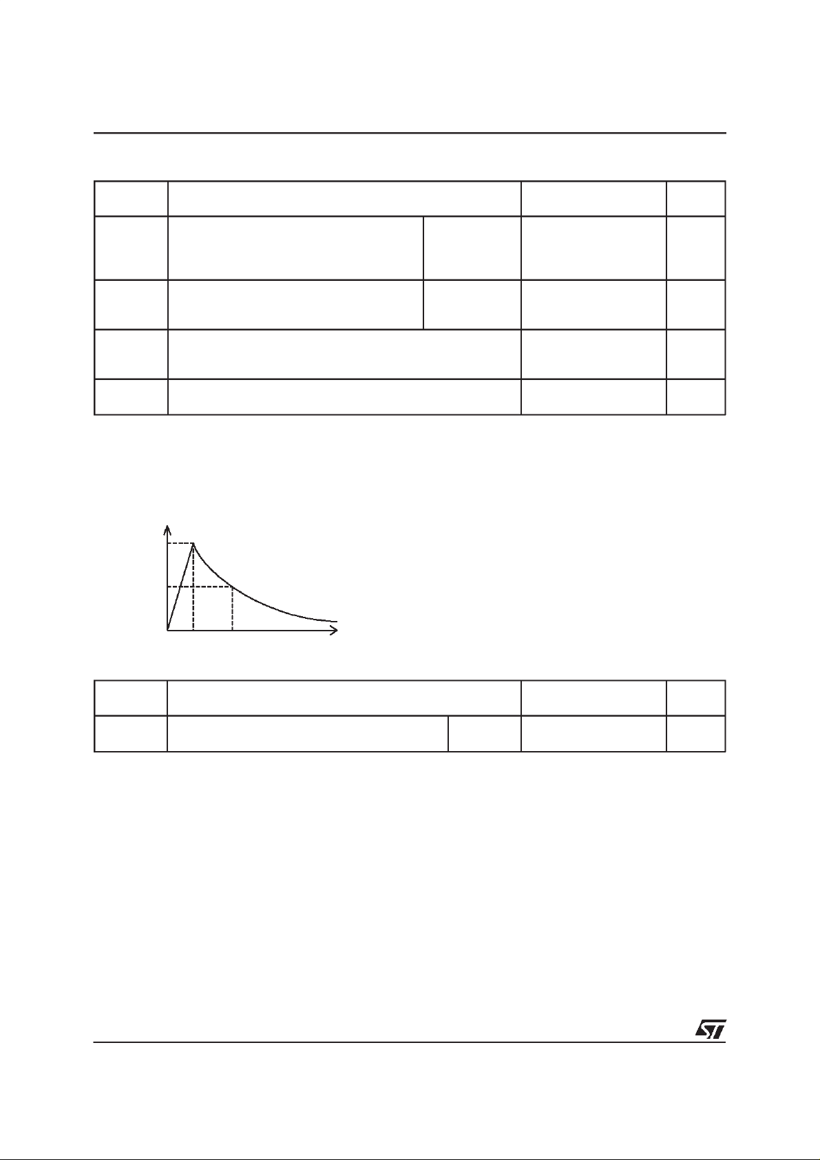
ABSOLUTE MAXIMUM RATINGS(T
amb
=25°C)
Symbol Parameter Value Unit
I
I
TSM
PP
Peak pulsecurrent (seenote 1)
Non repetitivesurge peak on-state
current (F = 50 Hz).
T
stg
T
j
T
L Maximumleadtemperaturefor solderingduring10s
Note 1 :
Storagetemperaturerange
Maximumjunctiontemperature
Pulse waveform :
10/1000µst
5/310µst
2/10µst
%I
PP
100
=10µst
r
=5µst
r
=2µst
r
=1000µs
p
=310µs
p
=10µs
p
10/1000µs
5/320µs
2/10 µs
tp= 10ms
t=1s
30
40
90
8
3.5
- 55 to + 150
150
260 °C
A
A
°C
50
0
t
t
rp
t
THERMAL RESISTANCES
Symbol Parameter Value Unit
R
th (j-a) Junctionto ambient
SO8 170
°
C/W
2/7
Page 3
TPI8011N/TPI12011N
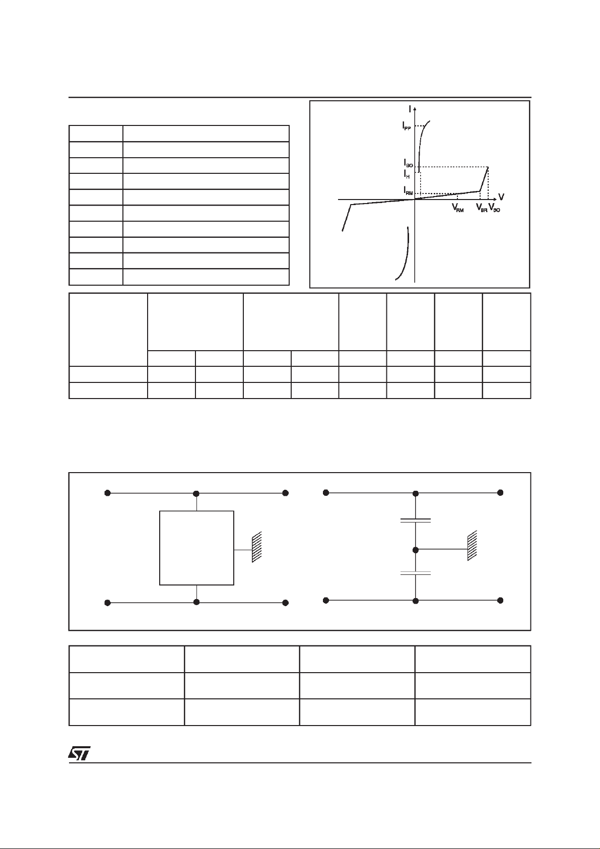
ELECTRICALCHARACTERISTICS
Symbol Parameter
V
RM Stand-offvoltage
I
RM Leakagecurrent
V
BR
V
BO
I
H
I
BO Breakovercurrent
I
PP Peakpulsecurrent
V
F ForwardVoltageDrop
C
Types
Breakdownvoltage
Breakovervoltage
Holdingcurrent
Capacitance
@V
I
RM
RM
max. min. max. typ. max. min.
µAV VmAV VmAmA
TPI8011N
TPI12011N
10 70 80 1 120 150 800 150
10 105 120 1 180 200 800 150
(
Tamb
=25°C)
VBR@I
R
V
BO
VBO
dyn.
I
BO
I
H
note1 note2 note1 note3
Note 1: Seethe reference testcircuit 1.
Note 2: Surgetest according toCCITT 1.5kV,10/700 µs betweenTip or Ringand ground.
Note 3: Seefunctional holding currenttest circuit2.
CAPACITANCES CHARACTERISTICS
LINE A
LINE A
TPIxx
LINE B
CONFIGURATION
=1V
V
A
=56V
V
B
V
=56V
A
=1V
V
B
(pF)
C
A
max
70 50 30
50 70 30
LINE B
CB(pF)
max
C
A
C
B
CA-CB(pF)
max
3/7
Page 4

TPI8011N/TPI12011N
REFERENCETESTCIRCUIT 1 :
TESTPROCEDURE:
PulseTestduration(tp = 20ms):
-For Bidirectionaldevices= SwitchKis closed
-For Unidirectionaldevices= SwitchKisopen.
Selection
V
OUT
-DevicewithV
-V
- Devicewith V
-V
BO
OUT
BO
OUT
< 200 Volt
=250V
≥ 200 Volt
=480V
RMS,R1
,R2= 240Ω.
RMS
= 140Ω.
FUNCTIONAL HOLDINGCURRENT(I
) TEST CIRCUIT 2 :
H
R
D.U.T .
V
= - 48 V
BAT
This isa GO-NOGOTestwhichallowstoconfirmthe holding current(I
testcircuit.
TESTPROCEDURE :
1) Adjustthecurrentlevel at theI
2) Firethe D.U.Twitha surgeCurrent: Ipp= 10A, 10/1000µs.
3) TheD.U.Twill comeback off-statewithin 50 ms max.
valueby short circuitingtheAKoftheD.U.T.
H
Surge generator
)levelin a functional
H
-V
P
4/7
Page 5

TPI8011N/TPI12011N
Fig. 1:
10
Surgepeakcurrentversusoverloadduration.
I (A)TSM
9
8
7
6
5
4
3
2
1
0
1E-2 1E-1 1E+0 1E+1 1E+2 1E+3
t(s)
F=50Hz
Tj initial=25°C
APPLICATIONNOTE.
Tip
GND
1
IN
2
3
OUT
8
Tip
7
GND
6
1) Connectpins2, 3, 6 and 7 to ground in order to guaranteeagoodsurgecurrent capability for longdurationdisturbances.
2) Inorder to take advantageof the ”4-point”
structureoftheTPIxxxN,the Tip and Ring
lines have to crossthedevice. In this case,the
devicewilleliminatethe overvoltagesgenerated by the parasiticinductancesof the wiring
(Ldi/dt),especiallyfor veryfast transients.
Ring
IN
4
OUT
5
Ring
4- point structurelay-out.
APPLICATIONCIRCUITS :
1 -UINTERFACE PROTECTION
A
TPIxx
B
RorPTC
RorPTC
GND
2 - S INTERFACEPROTECTION
A
TPIxx
B
A
TPIxx
B
GND
GND
RorPTC
RorPTC
RorPTC
RorPTC
This componentusesan intemalstructureresulting in symetricalcharacteristicswith a goodbalanced
behaviour.Itstopologyensures thesamebreakdownvoltagelevelforpositiveand negative surgesin
differentialand common mode.
5/7
Page 6

TPI8011N/TPI12011N
ORDERCODE
BIDIRECTIONAL
TPI 80 1 1 N RL
PACKAGING:
RL = Tape and reel
= Tube
REVISION
PACKAGE
1=SO8PLASTIC
BREAKDOWNVOLTAGE
MARKING
Package Type Marking
SO8 TPI8011N
TPI12011N
CONNECTIONDIAGRAM
SO8 Plastic
Tip
GND
GND
1
2
3
8
7
6
VERSION
TP80N
TP120N
Tip
GND
GND
6/7
Ring
4
5
Ring
Page 7

PACKAGEMECHANICALDATA
SO8 Plastic
TPI8011N/TPI12011N
DIMENSIONS
REF.
A 1.75 0.069
a1 0.1 0.25 0.004 0.010
a2 1.65 0.065
b 0.35 0.48 0.014 0.019
b1 0.19 0.25 0.007 0.010
C 0.50 0.020
c1 45°(typ)
D 4.8 5.0 0.189 0.197
E 5.8 6.2 0.228 0.244
e 1.27 0.050
e3 3.81 0.150
F 3.8 4.0 0.15 0.157
L 0.4 1.27 0.016 0.050
M 0.6 0.024
S8°(max)
Millimetres Inches
Min. Typ. Max. Min. Typ. Max.
Packaging: Productssuppliedinantistatictubes
or tape andreel.
Weight:
Informationfurnished is believedtobe accurateand reliable.However,STMicroelectronics assumes no responsibilityfor theconsequences of
use ofsuch informationnor forany infringement of patents orotherrightsof thirdparties which mayresult fromits use. No license isgranted by
implication or otherwise under any patent or patent rights of STMicroelectronics. Specifications mentioned in this publication are subject to
change without notice. Thispublication supersedesand replaces all information previously supplied.
STMicroelectronics products are not authorized for use as critical components in life support devices or systems withoutexpress written approval ofSTMicroelectronics.
Australia- Brazil- Canada- China -France -Germany- Italy- Japan -Korea- Malaysia- Malta-Mexico- Morocco -The
0.08g
1998 STMicroelectronics - Printed inItaly - Allrightsreserved.
STMicroelectronics GROUP OF COMPANIES
Netherlands - Singapore- Spain- Sweden- Switzerland- Taiwan-Thailand- UnitedKingdom- U.S.A.
7/7
 Loading...