

Page 1
General purpose JFET quad operational amplifier
Inverting Input 2
Non-inverting Input 2
Non-inverting Input 1
CC
V
-
CC
V
1
2
3
4
8
5
6
7
9
10
11
12
13
14
+
Output 3
Output 4
Non-inverting Input 4
Inverting Input 4
Non-inverting Input 3
Inverting Input 3
-
+
+
-
+
-
+
Output 1
Inverting Input 1
Output 2
Features
■ Wide common-mode (up to V
differential voltage range
■ Low input bias and offset current
■ Output short-circuit protection
■ High input impedance JFET input stage
■ Internal frequency compensation
■ Latch up free operation
■ High slew rate: 16V/µs (typ)
Description
The TL084, TL084A and TL084B are high-speed
JFET input quad operational amplifiers
incorporating well matched, high voltage JFET
and bipolar transistors in a monolithic integrated
circuit.
The devices feature high slew rates, low input
bias and offset currents, and low offset voltage
temperature coefficient.
CC
+
) and
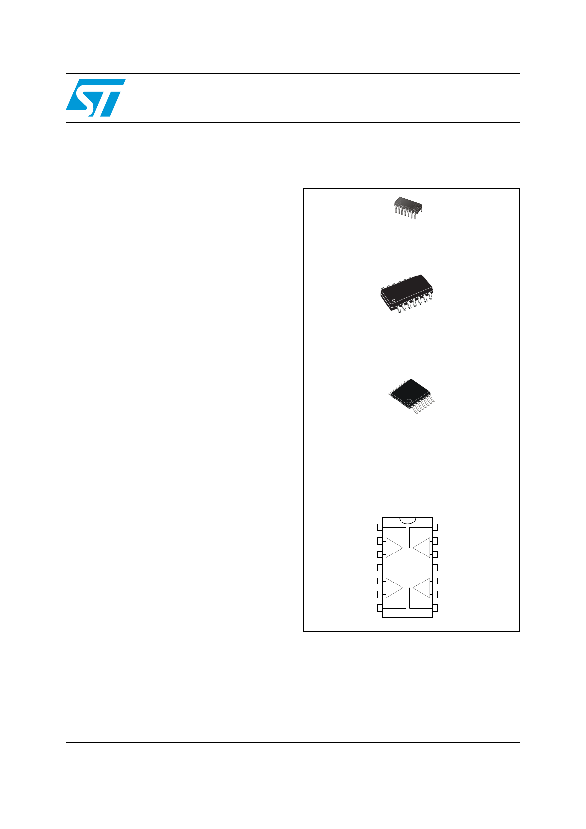
TL084
N
DIP14
(Plastic package)
D
TSSOP-14
(Thin shrink small outline package)
D
SO-14
(Plastic micropackage)
Pin connections
(Top view)
July 2007 Rev 2 1/16
www.st.com
16
Page 2
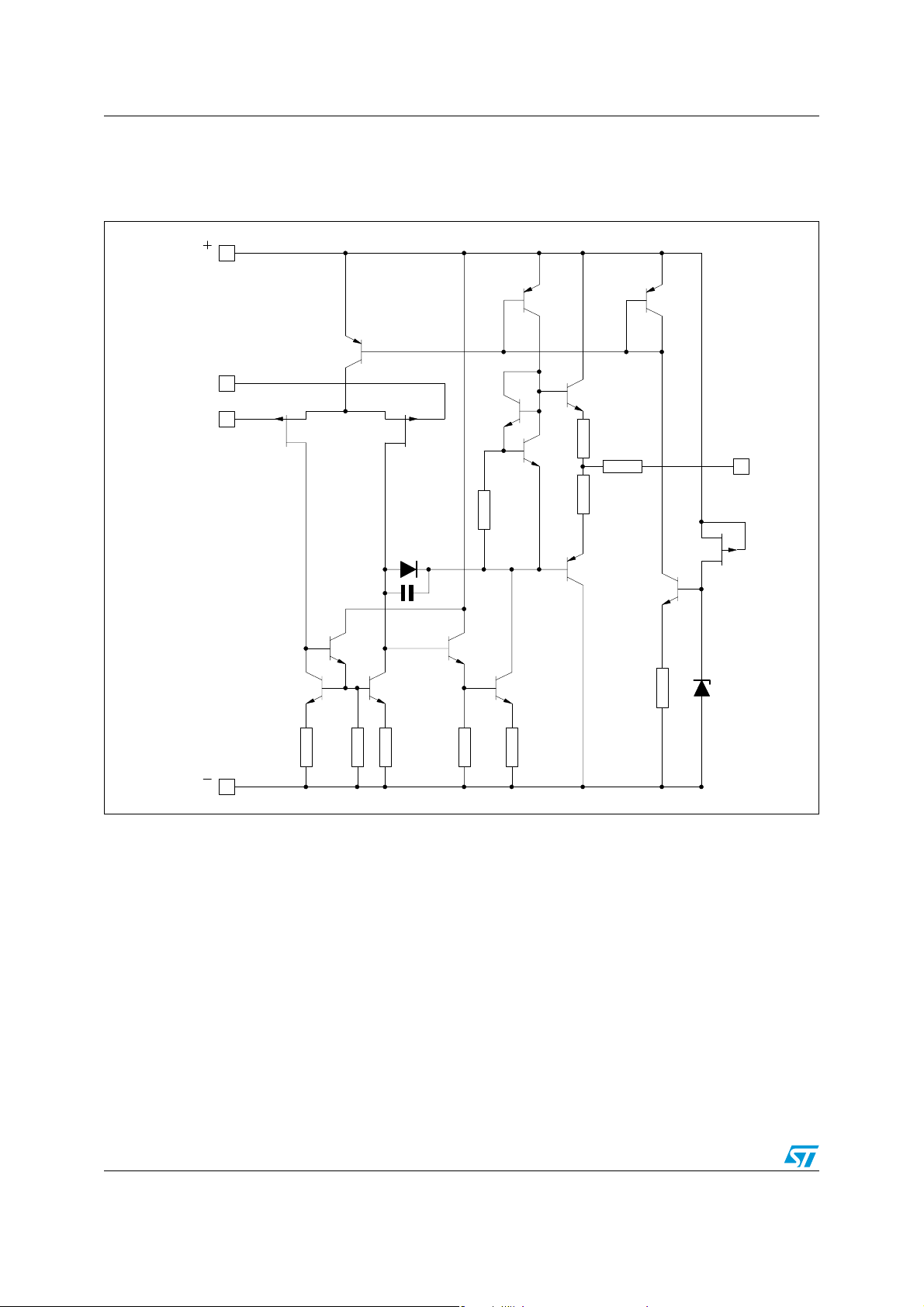
Schematic diagram TL084
1 Schematic diagram
Figure 1. Circuit schematics (for each amplifier)
V
CC
Non-inverting
input
Inverting
input
V
CC
1.3k
35k
1.3k
35k
30k
100
100
100
Ω
Ω
Ω
200
8.2k
Ω
Output
2/16
Page 3
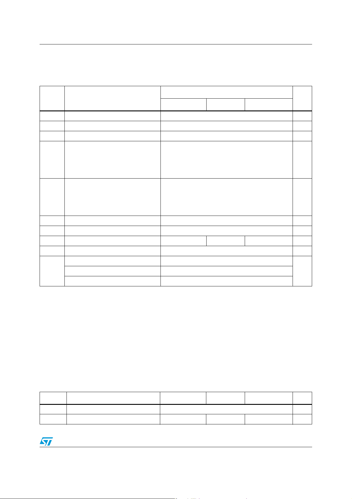
TL084 Absolute maximum ratings and operating conditions
2 Absolute maximum ratings and operating conditions
Table 1. Absolute maximum ratings
Value
Symbol Parameter
Unit
TL084M, AM, BM TL084I, AI, BI TL084C, AC, BC
(4) (5)
(2)
(1)
(8)
(3)
(7)
(6)
(9)
CC
+
and V
CC
±18 V
±15 V
±30 V
105
°C/W
80
100
31
°C/W
33
32
Infinite
1000
150
1500
-
.
V
Supply voltage
CC
V
Input voltage
i
Differential input voltage
V
id
Thermal resistance junction to
ambient
R
thja
SO-14
DIP14
TSSOP14
Thermal resistance junction to
(4) (5)
case
R
thjc
SO-14
DIP14
TSSOP14
P
Power dissipation 680 mW
tot
Output short-circuit duration
T
T
Operating free-air temperature range -55 to +125 -40 to +105 0 to +70 °C
oper
Storage temperature range -65 to +150 °C
stg
HBM: human body model
ESD
CDM: charged device model
1. All voltage values, except differential voltage, are with respect to the zero reference level (ground) of the supply voltages
where the zero reference level is the midpoint between V
2. The magnitude of the input voltage must never exceed the magnitude of the supply voltage or 15 volts, whichever is less.
3. Differential voltages are the non-inverting input terminal with respect to the inverting input terminal.
4. Short-circuits can cause excessive heating and destructive dissipation.
5. Rth are typical values.
6. The output may be shorted to ground or to either supply. Temperature and/or supply voltages must be limited to ensure
that the dissipation rating is not exceeded.
7. Human body model: 100pF discharged through a 1.5kΩ resistor between two pins of the device, done for all couples of pin
combinations with other pins floating.
8. Machine model: a 200pF cap is charged to the specified voltage, then discharged directly between two pins of the device
with no external series resistor (internal resistor < 5Ω), done for all couples of pin combinations with other pins floating.
9. Charged device model: all pins plus package are charged together to the specified voltage and then discharged directly to
the ground.
Table 2. Operating conditions
VMM: machine model
Symbol Parameter TL084M, AM, BM TL084I, AI, BI TL084C, AC, BC Unit
V
T
oper
Supply voltage range 6 to 36 V
CC
Operating free-air temperature range -55 to +125 -40 to +105 0 to +70 °C
3/16
Page 4

Electrical characteristics TL084
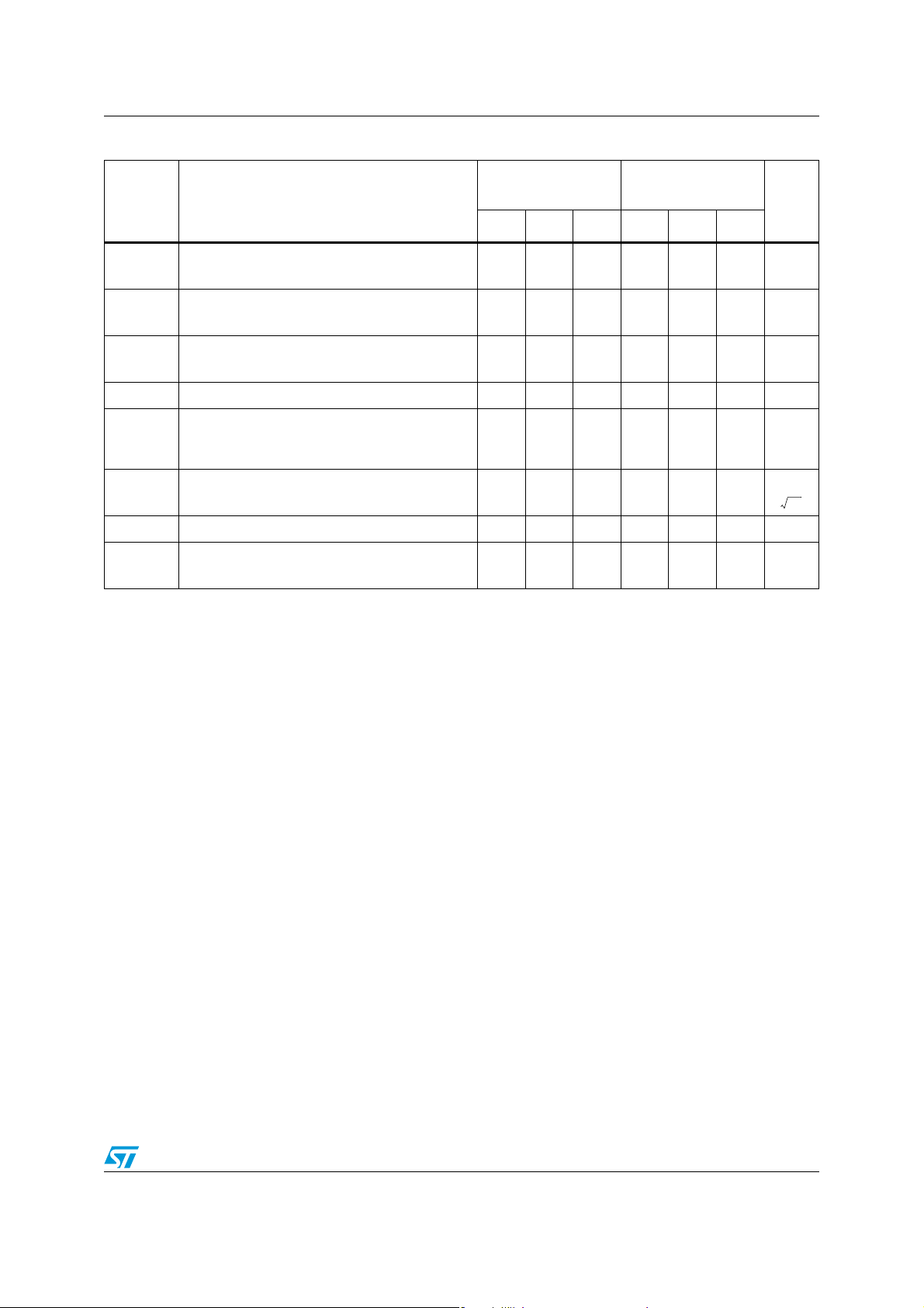
3 Electrical characteristics
Table 3. VCC = ±15V, T
= +25°C (unless otherwise specified)
amb
Symbol Parameter
Input offset voltage (Rs = 50Ω)
T
= +25°C TL084
amb
TL084A
V
io
≤ T
T
min
amb
≤ T
max
TL084B
TL084
TL084A
TL084B
DV
Input offset voltage drift 10 10 μV/°C
io
Input offset current
I
io
I
ib
= +25°C
T
amb
T
≤ T
amb
≤ T
min
Input bias current
T
= +25°C
amb
T
≤ T
amb
≤ T
min
max
(1)
max
Large signal voltage gain (RL = 2kΩ, Vo =±10V)
A
vd
T
T
amb
min
= +25°C
≤ T
amb
≤ T
max
Supply voltage rejection ratio (R
SVR
T
T
amb
min
= +25°C
≤ T
amb
≤ T
max
Supply current, no load
I
CC
V
icm
= +25°C
T
amb
≤ T
T
min
amb
≤ T
max
Input common mode voltage range
Common mode rejection ratio (RS = 50Ω)
CMR
T
T
amb
min
= +25°C
≤ T
amb
≤ T
max
Output short-circuit current
I
os
T
T
amb
min
= +25°C
≤ T
amb
≤ T
max
Output voltage swing
= +25°C RL = 2kΩ
T
±V
opp
SR
amb
T
≤ T
≤ T
min
amb
Slew rate (T
= 10V, RL = 2kΩ, CL = 100pF, unity gain
V
in
amb
RL = 2kΩ
max
= +25°C)
= 50Ω)
S
RL = 10kΩ
RL = 10kΩ
TL084I,M,AC,AI,AM,
BC,BI,BM
TL084C
Min. Typ. Max. Min. Typ. Max.
3
10
3
1
6
3
13
310
13
7
5
5100
4
20 200
20
5 100
4
30 200
20
5025200 2515200
80
86 70
80
1.4 2.5
±11 +15
-12
80
86 70
80
10
40 60
10
10
12
12
13.5
10
12
2.5
60
70
±11 +15
70
10
10
10
12
10
12
86 dB
1.4 2.5
2.5
-12
86
40 60
60
12
13.5
816 816 V/μs
Unit
mV
pA
nA
pA
nA
V/mV
mA
V
dB
mA
V
4/16
Page 5
TL084 Electrical characteristics
Table 3. VCC = ±15V, T
= +25°C (unless otherwise specified) (continued)
amb
TL084I,M,AC,AI,AM,
Symbol Parameter
BC,BI,BM
Min. Typ. Max. Min. Typ. Max.
t
r
K
ov
GBP
R
THD
e
n
Rise time (T
Vin = 20mV, RL = 2kΩ, CL = 100pF, unity gain
Overshoot (T
Vin = 20mV, RL = 2kΩ, CL = 100pF, unity gain
Gain bandwidth product (T
Vin = 10mV, RL = 2kΩ, CL = 100pF, f= 100kHz
Input resistance 10
i
Total harmonic distortion (T
f= 1kHz, RL = 2kΩ,CL = 100pF, Av = 20dB,
= 2Vpp)
V
o
Equivalent input noise voltage
= 100Ω, f = 1KHz
R
S
= +25°C)
amb
amb
= +25°C)
= +25°C)
amb
amb
0.1 0.1 μs
10 10 %
2.5 4 2.5 4 MHz
12
= +25°C,
0.01 0.01 %
15 15
∅m Phase margin 45 45
Vo1/V
Channel separation
o2
Av = 100
120 120 dB
TL084C
12
10
Unit
Ω
nV
----------- Hz
degrees
1. The input bias currents are junction leakage currents which approximately double for every 10°C increase in the junction
temperature.
5/16
Page 6

Electrical characteristics TL084
30
25
20
15
10
5
02468101214 16
MAXIMUM PEAK-TO-PEAK OUTPUT
VOLTAGE (V)
R
L
= 10 k
Ω
T
amb
= +25˚C
SUPPLY VOLTAGE ( V)
Figure 2. Maximum peak-to-peak output
voltage versus frequency
Figure 4. Maximum peak-to-peak output
voltage versus frequency
Figure 3. Maximum peak-to-peak output
voltage versus frequency
Figure 5. Maximum peak-to-peak output
voltage versus free air temperature
Figure 6. Maximum peak-to-peak output
voltage versus load resistance
Figure 7. Maximum peak-to-peak output
voltage versus supply voltage
6/16
Page 7

TL084 Electrical characteristics
1000
400
200
100
20
40
10
4
2
1
DIFFERENTIAL VOLTAGE
AMPLIFICATION (V/V)
-75 -50 -25 0
25 50 75
100
125
TEMPERATURE (˚C)
R
L
= 2k
Ω
V
O
= 10V
VCC= 15V
0
250
225
200
175
150
125
100
75
50
25
0
TOTAL POWER DISSIPATION (mW)
-75 -50 -25 0
25
50 75 100 125
TEMPERATURE (˚C)
V
CC
=
15V
No signal
No load
5
2.0
1.8
1.6
1.4
1.2
1.0
0.8
0.6
0.4
0.2
0
SUPPL Y CUR REN T (mA)
246810 12 14 16
No signal
No load
= +25˚C
T
amb
SUPPLY VOLTAGE ( V)
Figure 8. Input bias current versus free air
temperature
100
V
15V
=
CC
10
1
0.1
INPUT BIAS CURRENT (nA)
0.01
-50 -25 0 25 50 75 100 125
TEMPERATURE (˚C)
Figure 10. Large signal differential voltage
amplification and phase shift
versus frequency
100
PHASE SHIFT
(right scale)
10
R = 2k
C = 100pF
V = 15V
1
AMPLIFICATION (V/V)
DIFFERENTIAL VOLTAGE
T = +125°C
100
W
L
L
CC
amb
1K 10K 100K 10M1M
FREQUENCY (Hz)
DIFFERENTIAL
VOLTAGE
AMPLIFICATION
(left scale)
180
Figure 9. Large signal differential voltage
amplification versus free air
temperature
Figure 11. Total power dissipation versus free
air temperature
9
0
Figure 12. Supply current per amplifier versus
free air temperature
Figure 13. Supply current per amplifier versus
supply voltage
2.0
V
1.8
1.6
1.4
=
CC
No signal
No load
15V
1.2
1.0
0.8
0.6
0.4
0.2
SUPPLY CURRENT (mA)
0
-75 -50 -25 0
50 75 100 12
25
TEMPERATURE (˚C)
7/16
Page 8

Electrical characteristics TL084
70
60
50
40
30
20
10
0
EQUIVALENT INPU T NOISE
VOLTAGE (nV/VHz)
10 40 100 400 1k 4k 10k 40k 100k
FREQUENCY (Hz)
A
V
= 10
R
S
= 100
Ω
T
amb
= +25˚C
V
CC
= 15V
k
Figure 14. Common mode rejection ratio
COMMON MODE MODE REJECTION
Figure 15. Voltage follower large signal pulse
versus free air temperature
89
R
= 10 k
Ω
L
88
V
= 15V
CC
87
86
85
RATIO (dB)
(V)
84
83
-50 -25 0 25 50 75 100 125
-75
INPUT AND OUTPUT VOLTAGES
TEMPERATURE (˚C)
response
6
4
2
0
-2
-4
-6
0 0.5 1 1.5 2 2.5 3 3.5
V
CC
R
L
C
= 100pF
L
T
amb
= 2 k
OUTPUT
= 15V
W
= +25°C
TIME (ms)
INPUT
Figure 16. Output voltage versus elapsed time Figure 17. Equivalent input noise voltage
28
24
OVERSHOOT
20
90%
16
12
8
4
10%
0
OUTPUT VOLTAGE (mV)
-4
t
r
0 0.1 0.2
TIME (
0.3
V
= 15V
CC
R
= 2k
Ω
L
T
= +25˚C
amb
0.5
0.4
μ
s)
0.6
0.7
versus frequency
Figure 18. Total harmonic distortion versus
frequency
1
V
= 15V
V
= 15V
CC
0.4
0.1
0.04
(%)
0.01
0.004
0.001
TOTAL HARMONIC DISTORTION
8/16
CC
= 1
A
= 1
V
A
V
V
= 6V
V
= 6V
(rms)
O
(rms)
O
T
= +25˚C
= +25˚C
T
amb
amb
100 400 1k 4k 10k 40k 100
FREQUENCY (Hz)
Page 9

TL084 Typical applications
-
e
I
TL084
R
L
1/4
CL= 100pF
1k
Ω
10k
Ω
e
o
-
TL0 84
1/4
-
-
-
TL0 84
1/4
TL084
1/4
TL0 84
1/4
1M
Ω
1μF
Output A
Output B
Output C
Input
100k
Ω
100k
Ω
100k
Ω
100k
Ω
1OOμF
V
CC
+
f = 100kHz
O
Parameter measurement information
Figure 19. Voltage follower Figure 20. Gain-of-10 inverting amplifier
4 Typical applications
Figure 21. Audio distribution amplifier
9/16
Page 10

Typical applications TL084
Figure 22. Positive feeback bandpass filter
16k
Input
43k
1.5k
16k
Ω
220pF
43k
Ω
Ω
Ω
220pF
-
1/4
TL08 4
43k
Ω
-
1/4
TL08 4
30k
43k
1.5k
Ω
220pF
Ω
Ω
-
1/4
TL08 4
43k
220pF
Ω
43k
Ω
30k
Ω
Ω
-
1/4
TL08 4
Output B
Output A
Figure 23. Output A Figure 24. Output B
Second order bandpass filter
fo = 100kHz; Q = 30; Gain = 4
Cascaded bandpass filter
fo = 100kHz; Q = 69; Gain = 16
Ground
10/16
Page 11

TL084 Package information
5 Package information
In order to meet environmental requirements, ST offers these devices in ECOPACK®
packages. These packages have a lead-free second level interconnect. The category of
second level interconnect is marked on the package and on the inner box label, in
compliance with JEDEC Standard JESD97. The maximum ratings related t o soldering
conditions are also marked on the inner box label. ECOPACK is an ST trademark.
ECOPACK specifications are available at: www.st.com.
Figure 25. TSSOP14 package mech anical data
Dimensions
Ref.
Millimeters Inches
Min. Typ. Max. Min. Typ. Max.
A 1.2 0.047
A1 0.05 0.15 0.002 0.004 0.006
A2 0.8 1 1.05 0.031 0.039 0.041
b 0.19 0.30 0.007 0.012
c 0.09 0.20 0.004 0.0089
D 4.9 5 5.1 0.193 0.197 0.201
E 6.2 6.4 6.6 0.244 0.252 0.260
E1 4.3 4.4 4.48 0.169 0.173 0.176
e 0.65 BSC 0.0256 BSC
K0°8°0°8°
L 0.45 0.60 0.75 0.018 0.024 0.030
A2
A
A1
b
e
c
K
L
E
PIN 1 IDENTIFICATION
D
E1
1
11/16
Page 12

Package information TL084
Figure 26. DIP14 package mechanical data
Dimensions
Ref.
Min. Typ. Max. Min. Typ. Max.
a1 0.51 0.020
B 1.39 1.65 0.055 0.065
b0.5 0.020
b1 0.25 0.010
D200.787
E8.5 0.335
e 2.54 0.100
e3 15.24 0.600
F 7.1 0.280
I 5.1 0.201
L3.3 0.130
Z 1.27 2.54 0.050 0.100
Millimeters Inches
12/16
Page 13

TL084 Package information
Figure 27. SO-14 package mechanical data
Dimensions
Ref.
Min. Typ. Max. Min. Typ. Max.
A1.750.068
a1 0.1 0.2 0.003 0.007
a2 1.65 0.064
b 0.35 0.46 0.013 0.018
b1 0.19 0.25 0.007 0.010
C0.5 0.019
c1 45° (typ.)
D 8.55 8.75 0.336 0.344
E 5.8 6.2 0.228 0.244
e 1.27 0.050
e3 7.62 0.300
F 3.8 4.0 0.149 0.157
G 4.6 5.3 0.181 0.208
L 0.5 1.27 0.019 0.050
M0.680.026
S 8° (max.)
Millimeters Inches
13/16
Page 14

Ordering information TL084
6 Ordering information
Table 4. Order codes
Part number
TL084MN
TL084AMN
TL084BMN
TL084MD/MDT
TL084AMD/AMDT
TL084BMD/BMDT
TL084MP/MPT
TL084AMP/AMPT
TL084BMP/BMPT
TL084IN
TL084AIN
TL084BIN
TL084ID/IDT
TL084AID/AIDT
TL084BID/BIDT
TL084IP/IPT
TL084AIP/AIPT
TL084BIP/BIPT
TL084CN
TL084ACN
TL084BCN
Temperature
range
-55°C, +125°C
-40°C, +105°C
Package Packing Marking
TL084MN
DIP14 Tube
SO-14
TSSOP14
DIP14 Tube
SO-14
TSSOP14
DIP14 Tube
Tube or
tape & reel
Tube or
tape & reel
Tube or
tape & reel
Tube or
tape & reel
TL084AMN
TL084BMN
084M
084AM
084BM
084M
084AM
084BM
TL084IN
TL084AIN
TL084BIN
084I
084AI
084BI
084I
084AI
084BI
TL084CN
TL084ACN
TL084BCN
TL084CD/CDT
TL084ACD/ACDT
TL084BCD/BCDT
TL084CP/CPT
TL084ACP/ACPT
TL084BCP/BCPT
14/16
0°C, +70°C
SO-14
TSSOP14
Tube or
tape & reel
Tube or
tape & reel
084C
084AC
084BC
084C
084AC
084BC
Page 15

TL084 Revision history
7 Revision history
Table 5. Document revision history
Date Revision Changes
28-Mar-2001 1 Initial release.
, R
and ESD in Table 1: Absolute maximum
thjc
30-Jul-2007 2
Added values for R
thja
ratings.
Added Table 2: Operating conditions.
Expanded Table 4: Order codes.
Template update.
15/16
Page 16

TL084
Please Read Carefully:
Information in this document is provided solely in connection with ST products. STMicroelectronics NV and its subsidiaries (“ST”) reserve the
right to make changes, corrections, modifications or improvements, to this document, and the products and services described herein at any
time, without notice.
All ST products are sold pursuant to ST’s terms and conditions of sale.
Purchasers are solely res ponsibl e fo r the c hoic e, se lecti on an d use o f the S T prod ucts and s ervi ces d escr ibed he rein , and ST as sumes no
liability whatsoever relati ng to the choice, selection or use of the ST products and services described herein.
No license, express or implied, by estoppel or otherwise, to any intellectual property rights is granted under this document. If any part of this
document refers to any third pa rty p ro duc ts or se rv ices it sh all n ot be deem ed a lice ns e gr ant by ST fo r t he use of su ch thi r d party products
or services, or any intellectua l property c ontained the rein or consi dered as a warr anty coverin g the use in any manner whats oever of suc h
third party products or servi ces or any intellectual property contained therein.
UNLESS OTHERWISE SET FORTH IN ST’S TERMS AND CONDITIONS OF SALE ST DISCLAIMS ANY EXPRESS OR IMPLIED
WARRANTY WITH RESPECT TO THE USE AND/OR SALE OF ST PRODUCTS INCLUDING WITHOUT LIMITATION IMPLIED
WARRANTIES OF MERCHANTABILITY, FITNESS FOR A PARTICUL AR PURPOS E (AND THEIR EQUIVALE NTS UNDER THE LAWS
OF ANY JURISDICTION), OR INFRINGEMENT OF ANY PATENT, COPYRIGHT OR OTHER INTELLECTUAL PROPERTY RIGHT.
UNLESS EXPRESSLY APPROVED IN WRITING BY AN AUTHORIZED ST REPRESENTATIVE, ST PRODUCTS ARE NOT
RECOMMENDED, AUTHORIZED OR WARRANTED FOR USE IN MILITARY, AIR CRAFT, SPACE, LIFE SAVING, OR LIFE SUSTAINING
APPLICATIONS, NOR IN PRODUCTS OR SYSTEMS WHERE FAILURE OR MALFUNCTION MAY RESULT IN PERSONAL INJ URY,
DEATH, OR SEVERE PROPERTY OR ENVIRONMENTAL DAMAGE. ST PRODUCTS WHICH ARE NOT SPECIFIED AS "AUTOMOTIVE
GRADE" MAY ONLY BE USED IN AUTOMOTIVE APPLICATIONS AT USER’S OWN RISK.
Resale of ST products with provisions different from the statements and/or technical features set forth in this document shall immediately void
any warranty granted by ST fo r the ST pro duct or serv ice describe d herein and shall not cr eate or exten d in any manne r whatsoever , any
liability of ST.
ST and the ST logo are trademarks or registered trademarks of ST in various countries.
Information in this document su persedes and replaces all information previous ly supplied.
The ST logo is a registered trademark of STMicroelectronics. All other names are the property of their respective owners.
© 2007 STMicroelectronics - All rights reserved
STMicroelectronics group of compan ie s
Australia - Belgium - Brazil - Canada - China - Czech Republic - Finland - France - Germany - Hong Kong - India - Israel - Italy - Japan -
Malaysia - Malta - Morocco - Singapore - Spain - Sweden - Switzerland - United Kingdom - United States of America
www.st.com
16/16
 Loading...