

STMicroelectronics TDA7850A, TDA7850AH Schematic [ru]
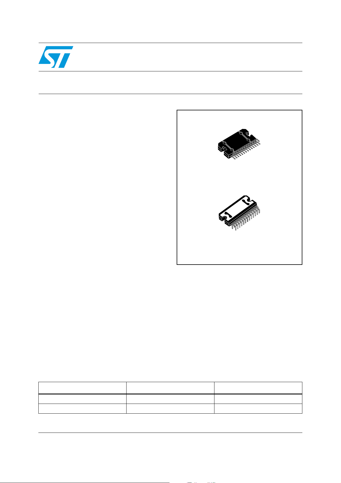
4 x 50 W MOSFET quad bridge power amplifier plus HSD
Features
■ High output power capability:
–4 x 50W/4Ω max.
–4 x 30W/4Ω @ 14.4V, 1KHz, 10%
–4 x 80W/2Ω max.
–4 x 55W/2Ω @ 14.4V, 1KHz, 10%
■ MOSFET output power stage
■ Excellent 2Ω driving capability
■ Hi-fi class distortion
■ Low output noise
■ St-by function
■ Mute function
■ Automute at min. supply voltage detection
■ Low external component count:
– Internally fixed gain (26dB)
– No external compensation
– No bootstrap capacitors
■ On board 0.35A high side driver
Protections:
■ Output short circuit to GND, to V
load
■ Very inductive loads
■ Overrating chip temperature with soft thermal
limiter
■ Output DC offset detection
■ Load dump voltage
■ Fortuitous open gnd
■ Reversed battery
Table 1. Device summary
, across the
s
TDA7850A
Flexiwatt27
(vertical)
Flexiwatt27
(horizontal)
■ ESD
Description
The TDA7850A is a breakthrough MOSFET
technology class AB audio power amplifier in
Flexiwatt27 package designed for high power car
radio. The fully complementary P-Channel/NChannel output structure allows a rail to rail
output voltage swing which, combined with high
output current and minimized saturation losses
sets new power references in the car-radio field,
with unparalleled distortion performances.
The TDA7850A integrates a DC offset detector.
Order code Package Packing
TDA7850A Flexiwatt27 (vertical) Tube
TDA7850AH Flexiwatt27 (horizontal Tube
October 2007 Rev 1 1/16
www.st.com
1

Contents TDA7850A
Contents
1 Block diagram and application circuit . . . . . . . . . . . . . . . . . . . . . . . . . . . 5
1.1 Block diagram . . . . . . . . . . . . . . . . . . . . . . . . . . . . . . . . . . . . . . . . . . . . . . . 5
1.2 Standard test and application circuit . . . . . . . . . . . . . . . . . . . . . . . . . . . . . 5
2 Pin description . . . . . . . . . . . . . . . . . . . . . . . . . . . . . . . . . . . . . . . . . . . . . 6
3 Electrical specifications . . . . . . . . . . . . . . . . . . . . . . . . . . . . . . . . . . . . . . 7
3.1 Absolute maximum ratings . . . . . . . . . . . . . . . . . . . . . . . . . . . . . . . . . . . . . 7
3.2 Thermal data . . . . . . . . . . . . . . . . . . . . . . . . . . . . . . . . . . . . . . . . . . . . . . . 7
3.3 Electrical characteristics . . . . . . . . . . . . . . . . . . . . . . . . . . . . . . . . . . . . . . . 7
3.4 Electrical characteristic curves . . . . . . . . . . . . . . . . . . . . . . . . . . . . . . . . . . 9
4 Application hints . . . . . . . . . . . . . . . . . . . . . . . . . . . . . . . . . . . . . . . . . . . 12
4.1 SVR . . . . . . . . . . . . . . . . . . . . . . . . . . . . . . . . . . . . . . . . . . . . . . . . . . . . . 12
4.2 Input stage . . . . . . . . . . . . . . . . . . . . . . . . . . . . . . . . . . . . . . . . . . . . . . . . 12
4.3 Stand-by and muting . . . . . . . . . . . . . . . . . . . . . . . . . . . . . . . . . . . . . . . . 12
4.4 DC offset detector . . . . . . . . . . . . . . . . . . . . . . . . . . . . . . . . . . . . . . . . . . 12
4.5 Heatsink definition . . . . . . . . . . . . . . . . . . . . . . . . . . . . . . . . . . . . . . . . . . 12
5 Package information . . . . . . . . . . . . . . . . . . . . . . . . . . . . . . . . . . . . . . . . 13
6 Revision history . . . . . . . . . . . . . . . . . . . . . . . . . . . . . . . . . . . . . . . . . . . 15
2/16

TDA7850A List of tables
List of tables
Table 1. Device summary . . . . . . . . . . . . . . . . . . . . . . . . . . . . . . . . . . . . . . . . . . . . . . . . . . . . . . . . . . 1
Table 2. Absolute maximum ratings . . . . . . . . . . . . . . . . . . . . . . . . . . . . . . . . . . . . . . . . . . . . . . . . . . 7
Table 3. Thermal data. . . . . . . . . . . . . . . . . . . . . . . . . . . . . . . . . . . . . . . . . . . . . . . . . . . . . . . . . . . . . 7
Table 4. Electrical characteristics . . . . . . . . . . . . . . . . . . . . . . . . . . . . . . . . . . . . . . . . . . . . . . . . . . . . 7
Table 5. Document revision history . . . . . . . . . . . . . . . . . . . . . . . . . . . . . . . . . . . . . . . . . . . . . . . . . 15
3/16

List of figures TDA7850A
List of figures
Figure 1. Block diagram . . . . . . . . . . . . . . . . . . . . . . . . . . . . . . . . . . . . . . . . . . . . . . . . . . . . . . . . . . . . 5
Figure 2. Standard test and application circuit. . . . . . . . . . . . . . . . . . . . . . . . . . . . . . . . . . . . . . . . . . . 5
Figure 3. Pin connection (top view) . . . . . . . . . . . . . . . . . . . . . . . . . . . . . . . . . . . . . . . . . . . . . . . . . . . 6
Figure 4. Quiescent current vs. supply voltage . . . . . . . . . . . . . . . . . . . . . . . . . . . . . . . . . . . . . . . . . . 9
Figure 5. Output power vs. supply voltage (R
Figure 6. Output power vs. supply voltage (R
Figure 7. Distortion vs. output power (R
Figure 8. Distortion vs. output power (R
Figure 9. Distortion vs. frequency (R
Figure 10. Distortion vs. frequency (R
= 4Ω) . . . . . . . . . . . . . . . . . . . . . . . . . . . . . . . . . . . . . . . . . . . 10
L
= 2Ω) . . . . . . . . . . . . . . . . . . . . . . . . . . . . . . . . . . . . . . . . . . . 10
L
Figure 11. Crosstalk vs. frequency . . . . . . . . . . . . . . . . . . . . . . . . . . . . . . . . . . . . . . . . . . . . . . . . . . . 10
Figure 12. Supply voltage rejection vs. frequency . . . . . . . . . . . . . . . . . . . . . . . . . . . . . . . . . . . . . . . . 10
Figure 13. Output attenuation vs. supply voltage. . . . . . . . . . . . . . . . . . . . . . . . . . . . . . . . . . . . . . . . . 10
Figure 14. Power dissipation & efficiency vs. output power (R
Figure 15. Power dissipation & efficiency vs. output power (R
Figure 16. Power dissipation vs. output power (R
Figure 17. Power dissipation vs. output power (R
Figure 18. ITU R-ARM frequency response, weighting filter for transient pop. . . . . . . . . . . . . . . . . . . 11
Figure 19. Flexiwatt27 (vertical) mechanical data and package dimensions . . . . . . . . . . . . . . . . . . . . 13
Figure 20. Flexiwatt27 (horizontal) mechanical data and package dimensions . . . . . . . . . . . . . . . . . . 14
= 4Ω) . . . . . . . . . . . . . . . . . . . . . . . . . . . . . . . . . . . . . 9
L
= 2Ω) . . . . . . . . . . . . . . . . . . . . . . . . . . . . . . . . . . . . . 9
L
= 4Ω). . . . . . . . . . . . . . . . . . . . . . . . . . . . . . . . . . . . . . . . . . 9
L
= 2Ω). . . . . . . . . . . . . . . . . . . . . . . . . . . . . . . . . . . . . . . . . 10
L
= 4Ω, SINE) . . . . . . . . . . . . . . . . . . . 11
L
= 2Ω, SINE) . . . . . . . . . . . . . . . . . . . 11
= 4Ω, audio program simulation) . . . . . . . . . . . . . 11
L
= 2Ω, audio program simulation) . . . . . . . . . . . . . 11
L
L
4/16
TDA7850A Block diagram and application circuit
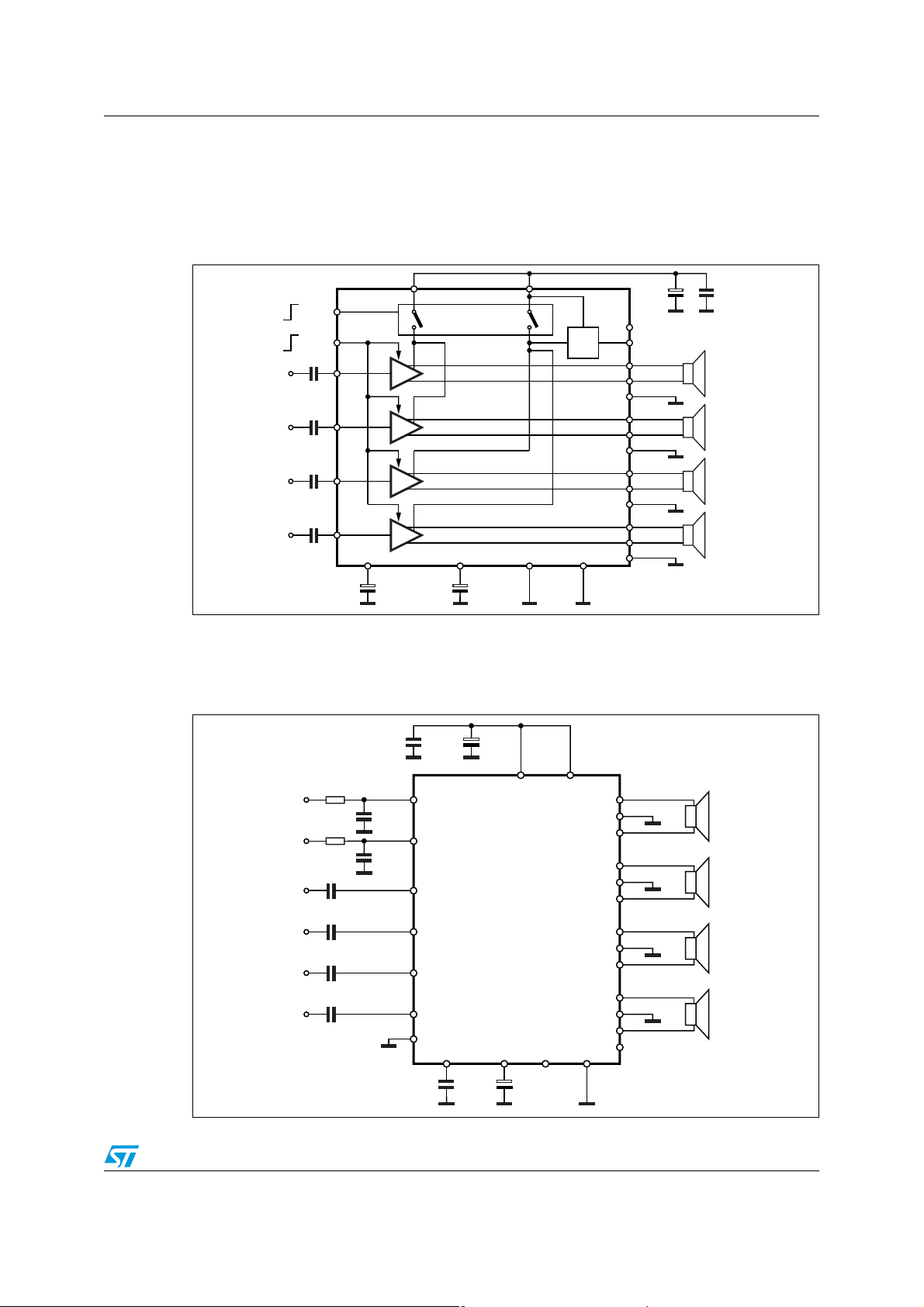
1 Block diagram and application circuit
1.1 Block diagram
Figure 1. Block diagram
IN1
IN2
IN3
IN4
ST-BY
MUTE
0.1μF
0.1μF
0.1μF
0.1μF
AC-GND
0.47μF47μF
Vcc1 Vcc2
OFF DET
HSD/OFF DETHSD
OUT1+
OUT1-
PW-GND
OUT2+
OUT2-
PW-GND
OUT3+
OUT3-
PW-GND
OUT4+
OUT4-
PW-GND
SVR TAB S-GND
D03AU1467
100nF470μF
1.2 Standard test and application circuit
Figure 2. Standard test and application circuit
ST-BY
MUTE
IN1
IN2
IN3
IN4
R1
10K
R2
47K
C1
0.1μF
C2 0.1μF
C3 0.1μF
C4 0.1μF
C9
1μF
C10
1μF
S-GND
C8
0.1μF
5
23
12
13
16
15
14
17 11 26 1, 27
C5
0.47μF
C7
2200μF
Vcc1-2
SVR TAB
C6
47μF
Vcc3-4
721
HSD/OFF DET
10
18
19
20
22
25
24
9
8
6
3
4
2
OUT1
OUT2
OUT3
OUT4
OFF DET
D03AU1469
5/16
Pin description TDA7850A
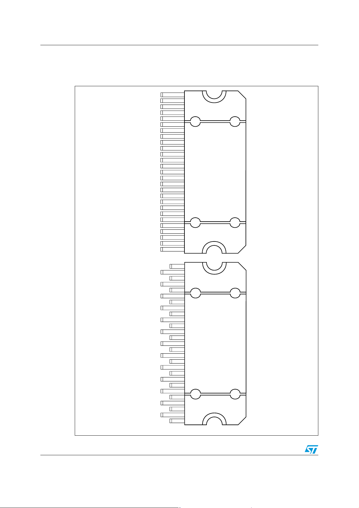
2 Pin description
Figure 3. Pin connection (top view)
TAB
OFF DET
PW-GND
OUT2-
ST-BY
OUT2+
V
OUT1-
PW-GND
OUT1+
SVR
IN1
IN2
S-GND
IN4
IN3
AC-GND
OUT3+
PW-GND
OUT3-
V
OUT4+
MUTE
OUT4-
PW-GND
HSD
TAB
TAB
OFF DET
PW-GND
OUT2-
ST-BY
OUT2+
V
OUT1-
PW-GND
OUT1+
SVR
IN1
IN2
S-GND
IN4
IN3
AC-GND
OUT3+
PW-GND
OUT3-
V
OUT4+
MUTE
OUT4-
PW-GND
HSD
TAB
1
CC
Vertical
CC
27
D03AU1468
1
CC
Horizontal
CC
27
AC00107
6/16
 Loading...