


UM2758
User manual
Evaluation board for TDA7803A and TDA7808 power amplifiers in PSO package
Introduction
Scope of this document is to describe the EVAL-7803APSO-SA standalone demo module.
It contains the module description, the schematic, the bill of materials and the board layout of the following modules:
6038-469.18 v1.0
In the following chapters it will be referred as 469 module.
UM2758 - Rev 1 - August 2020
For further information contact your local STMicroelectronics sales office.
www.st.com
1 Hardware description
1.1 Board description
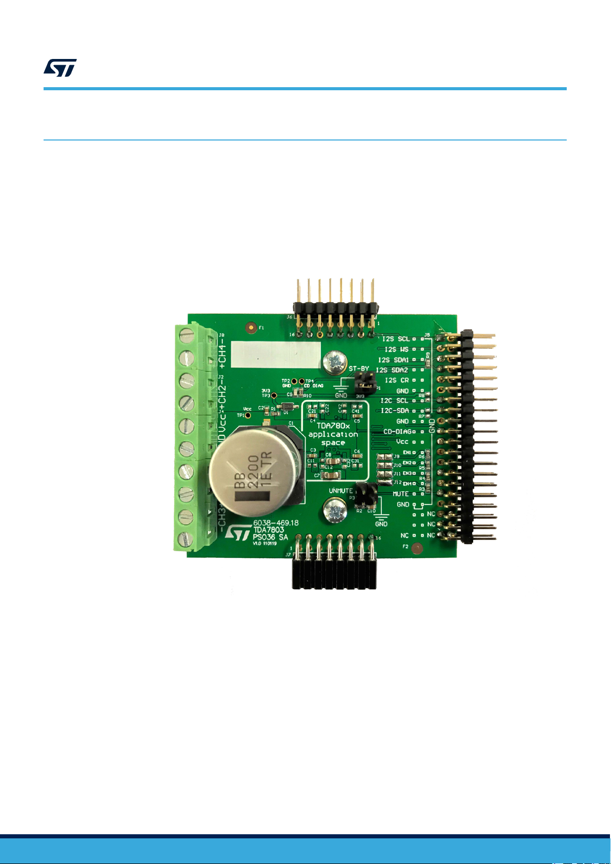
This board is based for TDA7803A and TDA7808 in PSO36 package. It is designed to provide 4 x 27 W on 4 Ω
load.
Figure 1. EVAL-7803APSO-SA board Top view
UM2758
Hardware description
UM2758 - Rev 1
page 2/13
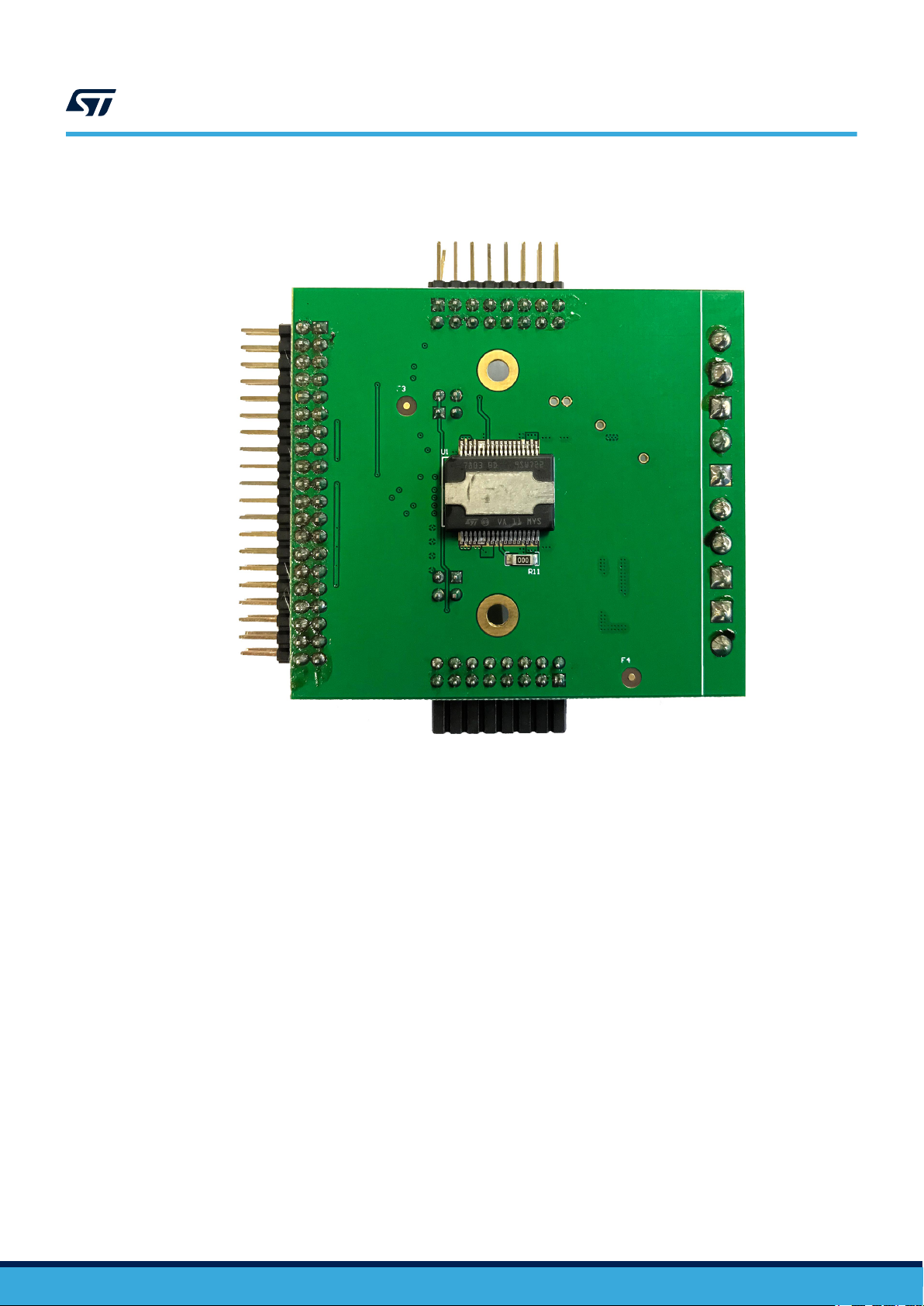
Figure 2. EVAL-7803APSO-SA board Bottom view
UM2758
Board description
Note: • Demo board are designed with scope to show typical device performance in standard application.
Furthermore, some components mounted on PCB could result downsized for satisfy a full performance
operation. Adequate heat dissipation must be provided for optimal performance: heatsink provided with
demo board ensures optimal dissipation when device is supplied with 14 V supply and a 4 Ω load is
connected to its outputs. For further information about high power measurements please contact ST
application team.
• The Figure 2 is taken without heatsink which is listed in the BOM reported in the Table 1.
UM2758 - Rev 1
page 3/13

1.2 Connector and connections
Power supply
The power supply, ranging from 4.5 V to 18.5 V, can be connected on J4 screw terminal following the labels.
Outputs
The amplifier outputs are present on J1, J2, J3, J8 screw terminal. The output assigned to each connection is
written nearby the connector
Input control signal
On J5 terminal is possible to find the I2C and I2S inputs. Additional control/monitor signals are available on this
connector: please refer to Section 1.3 Board option.
Board cascading
To test multiple device systems, is possible to connect more than one 469 modules together by means of J6 and
J7. Plugging J6 of one board to J7 of another, the I2C and I2S bus will be shared allowing to control the system by
means of one I2C interface and feed the same audio.
In order to command each device independently from each other, different addresses must be used on each 469
board. The number of 469 modules is limited by the maximum number of address that can be set.
1.3 Board option
UM2758
Connector and connections
Address selection
Proper I2C address for 469 module could be set by shorting with a 0 Ω resistor (or tin drop) one resistor from J9 to
J12. Please refer to TDA7901 datasheet for list of available addresses.
3.3 V voltage reference
On board 3.3 V reference (made by R1 and D1) is used for pull-up resistor of digital lines. When accurate current
measurement is needed (i.e. efficiency measurements) voltage reference should be disabled: in this case an
external 3.3v reference must be provided for 3V3 line.
STBY function
Stand by function can be hardware controlled by jumper P1 (3V3 →Device ON or GND → Device standby).
UNMUTE
Hardware unmute function is controlled by P3 (GND → device mute). By default these jumpers are left open
(device internal pull-up). P3 jumper allows also to remote control UNMUTE function through J10 connector (PIN
31, MUTE).
CD/DIAG
CD/DIAG function can be monitored through J10 connector, pin 19.
I2S data line pairing
If only one I2S data line is needed, SDA1 and SDA2 could be shorted through R9 with a 0 Ω (or tin drop).
1.4 Parallelized channels
TDA7803 provides the possibility to parallelize the channels to increase the output current capability. During this
operation one of the two channels in the parallel configuration will become the “Master” channel, the other one will
be the “Slave” channel.
The possible configurations are:
• CH1 and CH2 in parallel: CH1 is the master, CH2 is the slave
• CH3 and CH4 in parallel: CH3 is the master, CH4 is the slave
To use parallel configuration connect the two channels outputs close to the load, respecting output polarities.
Important:
When channels are parallelized, pay attention to the device’s configuration. Play signal with parallelized channels when the
device is configured for single output channels can lead to improper functioning
UM2758 - Rev 1
page 4/13

1.5 Board schematic
F1
P&P FiducialF2P&P Fiducial
F3
P&P FiducialF4P&P Fiducial
SH
1
HS1
SK1 SK2
BUSES EXP CONNECTORS
SCL
SDA
SCK
SDA2
SDA1
WS
SCK
WS
SDA1
SDA2
SCL
SDA
3V3
STD DONGLE CONNECT OR
TP3
TP2
SCL
SDA
SCK
SDA2
SDA1
WS
DGND
DGND
SDA2SDA1
DGND
CD/DIAG
TP4
DGND
DGND
SCK
WS
SDA1
SDA2
SCL
SDA
MUTE
OUT4-
OUT4+
OUT1-
OUT1+
OUT2+
OUT2-
OUT3+
OUT3-
OUTPUT CONNECT ORS
OUT1+
OUT1-
OUT2+
OUT2-
OUT3-
OUT3+
OUT4-
OUT4+
TAB
1
OUT4-
2
VCC34
3
PWGND4
4
OUT4+
5
NC
6
CD/DIAG
7
SDA
8
SCL
9
ADD
10
STDBY
11
WS
12
UNMUTEhw
13
OUT2+
14
PWGND2
15
VCC12
16
OUT2-
17
TAB
18
TAB
19
OUT1-
20
VCC12
21
PWGND1
22
OUT1+
23
SCK
24
SD24
25
SD13
26
DGND
27
AGND
28
D3V3
29
A3V3
30
NC
31
OUT3+
32
PWGND3+
33
VCC34
34
OUT3-
35
TAB
36
TDA
7803
U1
TDA7803
GND GND
GND GND
VCC34 VCC34
VCC12 VCC12
SCK
SDA
SCL
WS
OUT2+
OUT2-
GND
GND
OUT1-
OUT1+
GND
OUT3+
OUT3-
GND
SDA2
SDA1
CD/DIAG
OUT4-
OUT4+
DGND
3V3
112
2
334
4
P1
2x2 p2.54mm M
112
2
334
4
P3
2x2 p2.54mm M
DGND
DGND
DGND
GND
GND
ADD
MUTE
ADDR2 ADDR1 RES
0 0 R6
0 1 R5
1 0 R4
1 1 R3
R3 91K
R4 56K
R6 10K
R5 36K
J9 0R NM
J10 0R NM
J11 0R NM
J12 0R NM
DGND
ADD
C3
100nF
VCC12Vbatt
+
C1
2200uF
R1 1K
C4
100nF
VCC12
C5
100nF
VCC34
C6
100nF
VCC34
GND
3V3
GND AGND DGND
TP1
ADDRESS SELECTION NETWORK
D1
MMSZ5228BT1G
P4
Jumper
P2
Jumper
J1
J2
J3
J8
1 2
3 4
5 6
7 8
9 10
11 12
13 14
15 16
J6
8x2 p2.54mm M Horiz.
1 2
3 4
5 6
7 8
9 10
11 12
13 14
15 16
J7
8x2 p2.54mm F Horiz.
2
4
6
8
10
1
3
5
7
9
11 12
13 14
15 16
17 18
19 20
21 22
23 24
25 26
27 28
29 30
31 32
33 34
35 36
37 38
39 40
J5
20x2 p2.54mm M Horiz.
J4
C11
4.7nF NM
C12
4.7nF NM
C31
4.7nF NM
C32
4.7nF NM
C41
4.7nF NM
C42
4.7nF NM
C22
4.7nF NM
C21
4.7nF NM
C7
22uF
C8
4.7uF
R11 0R
C10
1uF
R2 47K
R9
0R NM
R8
4K7 NM
R7
4K7 NM
R10 47K
C9
100pF
POWER ST AGE
C2
220nF
UM2758
Board schematic
Figure 3. EVAL-7803APSO-SA board schematic
UM2758 - Rev 1
page 5/13

1.6 Bill of materials
Quantity Designator Description Value Rated V Package
1 C1 SMD Electrolityc Capacitor 2200 uF 25 V 19x19 d18 mm
1 C2 SMD MLCC X7R Capacitor 220 nF 25 V 0603
4 C3, C4, C5, C6 SMD MLCC X7R Capacitor 100 nF 25 V 0603
1 C7 SMD MLCC X7R Capacitor 22 uF 6.3 V 1206
1 C8 SMD MLCC X7R Capacitor 4.7 μF 10 V 0805
1 C9 SMD MLCC X7R Capacitor 100 pF 16 V 0603
1 C10 SMD MLCC X7R Capacitor 1 μF 25 V 0805
C11, C12, C21, C22, C31,
8
1 D1 3.9V Zener DIODE - 3.9 V SOD-123
1 HS1 HEATSINK - - -
5 J1, J2, J3, J4, J8 Terminal Block 2position p5.08mm - - p5.08 mm
1 J5 Header, 40-Pin, Dual row, TH, Right Angle, Male - - p2.54 mm
1 J6 Header, 8-Pin, Dual row, TH, Right Angle, Male - - p2.54 mm
1 J7 Header, 8-Pin, Dual row, TH, Right Angle, Female - - p2.54 mm
4 J9, J10, J11, J12 Solder Jumper 0805 - - 0805
2 P1, P3 Header, 2-Pin, Dual row, TH, Straight, Male - - p2.54 mm
2 P2, P4 Jumper shunt p2.54mm - - p2.54 mm
1 R1 Surface mount chip resistor 1 KΩ 75 V 0603
1 R2 Surface mount chip resistor 47 KΩ 75 V 0603
1 R3 Surface mount chip resistor 91 KΩ 75 V 0603
1 R4 Surface mount chip resistor 56 KΩ 75 V 0603
1 R5 Surface mount chip resistor 36 KΩ 75 V 0603
1 R6 Surface mount chip resistor 10 KΩ 75 V 0603
2 R7, R8 Surface mount chip resistor 4.7 KΩ 75 V 0603
1 R9 Surface mount chip resistor 0 Ω 75 V 0603
1 R10 Surface mount chip resistor 47 KΩ 75 V 0603
1 R11 Surface mount chip resistor 0 Ω 200 V 1206
2 SK1, SK2 M3 Fastener - - -
1 U1 4 Channel Class AB Amplifier - - PSO36
C32, C41, C42
UM2758
Bill of materials
Table 1. Bill of materials
SMD MLCC X7R Capacitor 4 n7 25 V 0603
UM2758 - Rev 1
page 6/13

1.7 Board layout
UM2758
Board layout
Figure 4. Assembly top
Figure 5. Inner 1
UM2758 - Rev 1
page 7/13

Figure 6. inner 2
UM2758
Board layout
Figure 7. Assembly bottom
UM2758 - Rev 1
page 8/13

2 Information on board use
This evaluation board/kit is intended to be used for ENGINEERING DEVELOPMENT, DEMONSTRATION OR
EVALUATION PURPOSES ONLY and it is not considered by ST Microelectronics (ST) a finished end product fit
for general consumer use. People handling the product(s) must have electronics training and observe good
engineering practice standards. As such, the goods being provided are not intended to be complete in terms of
required design-, marketing- and/or manufacturing-related protective considerations, including product safety and
environmental measures typically found in end products that incorporate such semiconductor components or
circuit boards. This evaluation board/kit does not fall within the scope of the European Union directives regarding
electromagnetic compatibility, restricted substances (RoHS), recycling (WEEE), FCC, CE or UL, and therefore
they may not meet the technical requirements of these directives or other related directives.
UM2758
Information on board use
UM2758 - Rev 1
page 9/13

Revision history
UM2758
Table 2. Document revision history
Date Version Changes
05-Aug-2020 1 Initial release.
UM2758 - Rev 1
page 10/13

UM2758
Contents
Contents
1 Hardware description ..............................................................2
1.1 Board description ..............................................................2
1.2 Connector and connections ......................................................4
1.3 Board option ..................................................................4
1.4 Parallelized channels ...........................................................4
1.5 Board schematic ...............................................................5
1.6 Bill of materials ................................................................6
1.7 Board layout...................................................................7
2 Information on board use ..........................................................9
Revision history .......................................................................10
UM2758 - Rev 1
page 11/13

UM2758
List of figures
List of figures
Figure 1. EVAL-7803APSO-SA board Top view ....................................................2
Figure 2. EVAL-7803APSO-SA board Bottom view ..................................................3
Figure 3. EVAL-7803APSO-SA board schematic ...................................................5
Figure 4. Assembly top .....................................................................7
Figure 5. Inner 1..........................................................................7
Figure 6. inner 2..........................................................................8
Figure 7. Assembly bottom ..................................................................8
UM2758 - Rev 1
page 12/13

UM2758
IMPORTANT NOTICE – PLEASE READ CAREFULLY
STMicroelectronics NV and its subsidiaries (“ST”) reserve the right to make changes, corrections, enhancements, modifications, and improvements to ST
products and/or to this document at any time without notice. Purchasers should obtain the latest relevant information on ST products before placing orders. ST
products are sold pursuant to ST’s terms and conditions of sale in place at the time of order acknowledgement.
Purchasers are solely responsible for the choice, selection, and use of ST products and ST assumes no liability for application assistance or the design of
Purchasers’ products.
No license, express or implied, to any intellectual property right is granted by ST herein.
Resale of ST products with provisions different from the information set forth herein shall void any warranty granted by ST for such product.
ST and the ST logo are trademarks of ST. For additional information about ST trademarks, please refer to www.st.com/trademarks. All other product or service
names are the property of their respective owners.
Information in this document supersedes and replaces information previously supplied in any prior versions of this document.
© 2020 STMicroelectronics – All rights reserved
UM2758 - Rev 1
page 13/13
 Loading...