

STMicroelectronics TDA7496 Schematic [ru]
TDA7496
5W+5W AMPLIFIER WITH DC VOLUME CONTROL
5+5WOUTPUTPOWER
R
=8Ω@THD= 10% VCC= 22V
L
ST-BYAND MUTEFUNCTIONS
LOW TURN-ON TURN-OFF POP NOISE
LINEAR VOLUME CONTROL DC COUPLED
WITH POWEROP. AMP.
NO BOUCHEROTCELL
NO ST-BY RC INPUT NETWORK
SINGLESUPPLYRANGINGUP TO35V
SHORTCIRCUITPROTECTION
THERMALOVERLOAD PROTECTION
INTERNALLYFIXED GAIN
SOFTCLIPPING
VARIABLE OUTPUT AFTER VOLUME CON-
TROL CIRCUIT
MULTIWATT 15 PACKAGE
DESCRIPTION
The TDA7496 is a stereo 5+5W class AB power
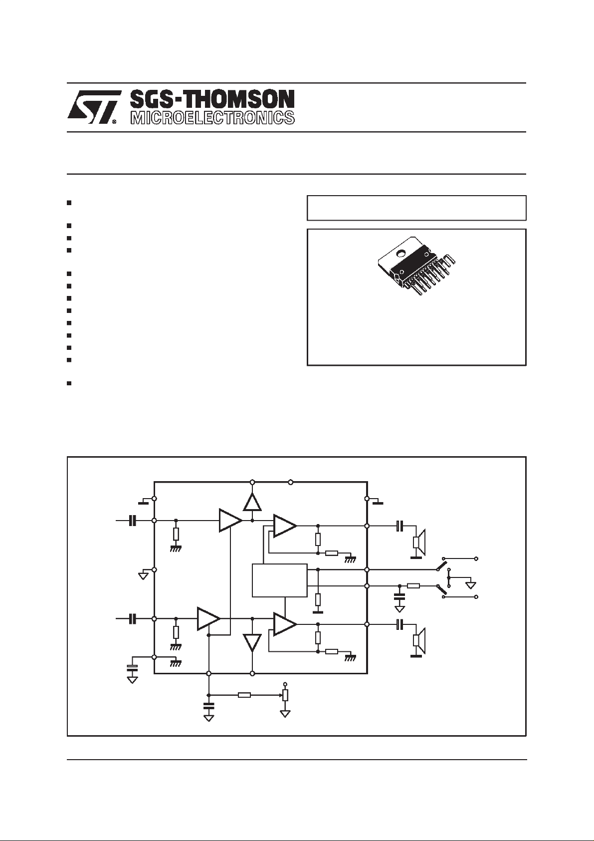
BLOCK AND APPLICATIONDIAGRAM
VAROUT_R
2
PROTECTIONS
VAROUT_L
+
OP AMP
MUTE/STBY
+
-30K
OP AMP
INR
INL
470µF
PW_GND
470nF
S_GND
470nF
SVR 7
11
1
8
5
VOLUME
30K
VOLUME
34
VOLUME
MULTIPOWERBI50IITECHNOLOGY
Multiwatt15
ORDERING NUMBER: TDA7496
amplifier assembled in the @ Multiwatt 15 package, specially designed forhigh quality sound, TV
applications.
Features of the TDA7496 include linear volume
control, Stand-byandmute functions.
V
S
13
60K
+5V
15
14
10
12
9
PW_GND
1000µF
OUTR
STBY
MUTE
OUTL
1000µF
10K
1µF
S1 ST-BY
S2 MUTE
+5V
S_GND
+5V
April 1998
100nF
300K
D96AU440D
1/10
TDA7496
ABSOLUTE MAXIMUM RATINGS
Symbol Parameter Value Unit
V
S
V
IN
P
tot
amb Ambient Operating Temperature 0 to 70 °C
T
T
stg,Tj
V
3
DC Supply Voltage 35 V
Maximum Input Voltage 8 Vpp
Total Power Dissipation (Tamb = 80°C) 15 W
Storage and Junction Temperature -40 to 150 °C
Volume CTRL DC voltage 7 V
PIN CONNECTION
(Top view)
15
14
13
12
11
10
9
8
7
6
5
4
3
2
1
D96AU441B
PW_GND
OUTR
V
S
OUTL
PW_GND
MUTE
STBY
S_GND
SVR
N.C.
INL
VAROUT_L
VOLUME
VAROUT_R
INR
THERMAL DATA
Symbol Parameter Value Unit
R
th j-case
R
th j-amb
Thermal Resistance Junction-case Typ. = 4 Max. = 4.6 °C/W
Thermal Resistance Junction-ambient max 35 °C/W
ELECTRICALCHARACTERISTICS
(RefertothetestcircuitV
= 22V; RL=8Ω,Rg=50Ω,T
S
amb
=25°C).
Symbol Parameter Test Condition Min. Typ. Max. Unit
V
DCV
S
I
q
Supply Voltage Range 10 32 V
Total Quiescent Current 25 50 mA
OS Output DC Offset Referred to
No Input Signal 200 mV
SVR Potenial
V
O
P
O
THD Total Harmonic Distortion G
I
peak
V
in
G
V Closed Loop Gain Vol Ctrl > 4.5V 28.5 30 31.5 dB
Quiescent Output Voltage 11 V
Output Power THD= 10%;RL=8Ω; 5 5.5 W
THD= 1%;R
THD= 10%;R
THD= 1%;R
= 30dB;PO= 1W; f = 1KHz; 0.4 %
V
=8Ω;4W
L
=4Ω;VCC= 12V 2.1 W
L
=4Ω;VCC= 12V 1.0 W
L
Output Peak Current (internally limited) 1 1.3 A
Input Signal 2.8 Vrms
2/10
TDA7496
ELECTRICALCHARACTERISTICS (continued)
Symbol Parameter Test Condition Min. Typ. Max. Unit
G
vLine
A
MinVOL
BW 0.6 MHz
e
N
SR Slew Rate 5 8 V/µs
R
R
Var Out Variable Output Resistance 30 100 Ω
R
load Var Out Variable Output Load 2 KΩ
SVR Supply Voltage Rejection f = 1kHz; max volume
T
M
T
s
MUTE STAND-BY & INPUT SELECTION FUNCTIONS
V
ST-ON
V
ST-OFF
V
MON Mute ON Threshold 3.5 V
V
M OFF
I
qST-BY
A
MUTE
I
stbyBIAS Stand-by bias current Stand by on VST-BY =5V
I
muteBIAS
Monitor Out Gain Vol Ctrl > 4.5V; Zload > 30KΩ -1.5 0 1.5 dB
Attenuation at Minimum Volume Vol Ctrl < 0.5V 80 dB
Total Output Noise f = 20Hz to 22KHz
500 800 µV
Play, max volume
f = 20Hz to 22KHz
100 250 µV
Play, max attenuation
f = 20Hz to 22KHz
60 150 µV
Mute
Input Resistance 22.5 30 K
i
35 39 dB
C
= 470µF;VRIP =1Vrms
SVR
f = 1kHz; max attenuation
C
= 470µF;V
SVR
RIP
=1V
rms
55 65 dB
Thermal Muting 150 °C
Thermal Shut-down 160 °C
Stand-by ON threshold 3.5 V
Stand-by OFF threshold 1.5 V
Mute OFF Threshold 1.5 V
Quiescent Current @ Stand-by 0.6 1 mA
Mute Attenuation 50 65 dB
80 µA
V
=5V
MUTE
Play or Mute -20 -5 µA
Mute bias current Mute 1 5 µA
Play 0.2 2
Ω
A
µ
A
µ
APPLICATIONSUGGESTIONS
The recommended values of theexternal components are those shown on the application circuit of figure 1a. Differentvaluescan be used, the followingtablecan help the designer.
COMPONENT
SUGGESTION
VALUE
PURPOSE
R1 300K Volume controlcircuit
R2 10K Mute time constant Larger mute on/off time Smaller mute on/off time
P1 50K Volume control circuit
C1 1000µF
Supply voltage
bypass
C2 470nF Input DC decoupling Lower low frequency cutoff Higher low frequency cutoff
C3 470nF Input DC decoupling Lower low frequency cutoff Higher low frequency cutoff
C4 470µF Ripple rejection Better SVR Worse SVR
C5 100nF
Volume controltime
costant
C6 1000µF OutputDC decoupling Lower low frequency cutoff Higher low frequency cutoff
C7 1µF Mute time costant Larger mute on/off time Smaller mute on/off time
C8 1000µF OutputDC decoupling Lower low frequency cutoff Higher low frequency cutoff
C9 100nF
Supply voltage
bypass
LARGER THAN
SUGGESTION
Larger volume regulation
time
Larger volume regulation
time
SMALLER THAN
SUGGESTION
Smaller volume regulation
time
Danger of oscillation
Smaller volume regulation
time
Danger of oscillation
3/10
TDA7496
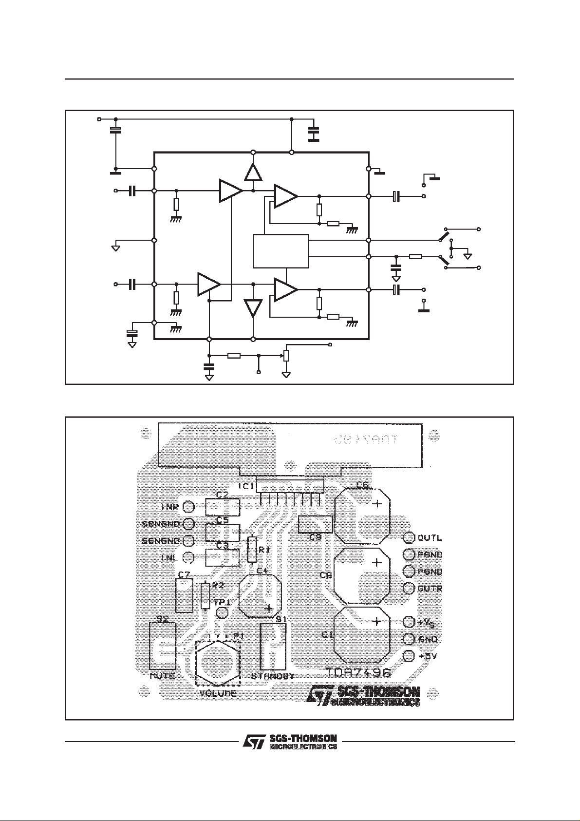
Figure 1a:
+V
S
INR
INL
C4 470µF
ApplicationCircuit.
C1
1000µF
PW_GND
C2 470nF
S_GND
C3 470nF
11
1
30K
8
5
SVR 7
VOLUME
100nF
VAROUT_R
VOLUME
VOLUME
34
VAROUT_L
C5
R1 300K
2
+
OP AMP
MUTE/STBY
PROTECTIONS
+
-30K
OP AMP
TP1
C9
0.1µF
V
S
13
VOL
P1
50K
LOG
+5V
15
14
10
12
9
PW_GND
C8 1000µF
C7
1µF
C6 1000µF
R2 10K
PW_GND
OUTR
OUTL
PW_GND
D96AU493D
S1 STBY
S2 MUTE
+5V
S_GND
+5V
Figure 1b:
P.C.B.and Component Layout.
4/10
 Loading...