STMicroelectronics TDA7293 Schematic [ru]

TDA7293
120V - 100W DMOS AUDIO AMPLIFIER WITHMUTE/ST-BY
VERY HIGH OPERATING VOLTAGE RANGE
(±50V)
DMOSPOWERSTAGE
HIGH OUTPUT POWER (100W @ THD =
10%, R
L =8
,VS=±40V)
Ω
MUTING/STAND-BYFUNCTIONS
NO SWITCHON/OFF NOISE
VERYLOW DISTORTION
VERYLOW NOISE
SHORT CIRCUIT PROTECTED (WITHNO IN-
PUT SIGNAL APPLIED)
THERMALSHUTDOWN
CLIPDETECTOR
MODULARITY (MORE DEVICES CAN BE
EASILY CONNECTED IN PARALLEL TO
DRIVE VERYLOW IMPEDANCES)
DESCRIPTION
The TDA7293 is a monolithic integrated circuit in
Multiwatt15 package, intended for use as audio
class AB amplifier in Hi-Fi field applications
(Home Stereo, self powered loudspeakers, Top-
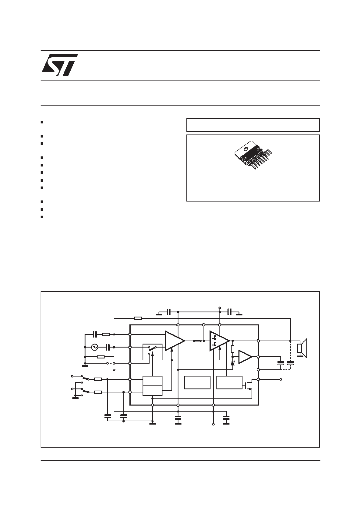
Figure 1: Typical Applicationand Test Circuit
MULTIPOWER BCD TECHNOLOGY
Multiwatt15
ORDERING NUMBER: TDA7293V
class TV). Thanks to the wide voltage range and
to the high out current capability it is able to supply the highest powerinto both4Ω and 8Ω loads.
The built in muting function with turn on delay
simplifiesthe remote operation avoiding switching
on-off noises.
Parallel mode is made possible by connecting
more device through of pin11. High output power
can be deliveredto verylow impedance loads, so
optimizingthe thermal dissipation ofthe system.
VMUTE
VSTBY
October 2000
C7 100nF C6 1000µF
R3 22K
C2
R2
22µF
680Ω
C1 470nF
R1 22K
R5 10K
R4 22K
C3 10µFC410µF
IN- 2
IN+
3
4
SGND
(**)
10
MUTE
9
STBY
(*) see Application
(**) for SLAVE function
note
MUTE
STBY
1
STBY-GND
+Vs
BUFFER DRIVER
713
11
-
+
THERMAL
SHUTDOWN
-Vs -PWVs
C9 100nF C8 1000µF
PROTECTION
158
-Vs
+PWVs+Vs
S/C
14
12
6
5
D97AU805A
OUT
BOOT
LOADER
C5
22µF
BOOTSTRAP
CLIP DET
(*)
VCLIP
1/13

TDA7293
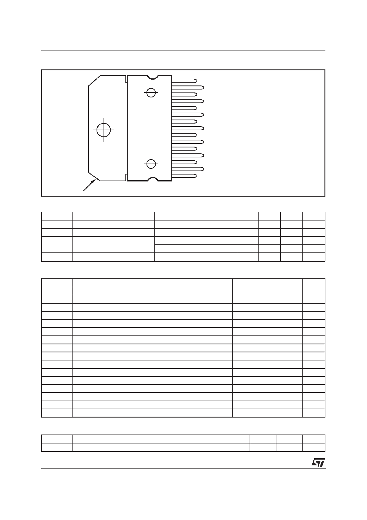
PIN CONNECTION (Top view)
TAB CONNECTED TO PIN 8
15
14
13
12
11
10
9
8
7
6
5
4
3
2
1
D97AU806
-VS(POWER)
OUT
(POWER)
+V
S
BOOTSTRAP LOADER
BUFFER DRIVER
MUTE
STAND-BY
-V
(SIGNAL)
S
+VS(SIGNAL)
BOOTSTRAP
CLIP AND SHORT CIRCUIT DETECTOR
SIGNAL GROUND
NON INVERTING INPUT
INVERTING INPUT
STAND-BY GND
QUICK REFERENCEDATA
Symbol Parameter Test Conditions Min. Typ. Max. Unit
V
S
G
LOOP
P
tot
SVR Supply Voltage Rejection 75 dB
Supply Voltage Operating ±12 æ 50 V
Closed Loop Gain 26 40 dB
Output Power VS=±45V; RL=8Ω; THD = 10% 140 W
= ±30V; RL =4Ω; THD = 10% 110 W
V
S
ABSOLUTE MAXIMUM RATINGS
Symbol Parameter Value Unit
V
S
V
V
2 -V3 Maximum Differential Inputs ±30 V
V
V
V
V
V
V
V
10
11 Buffer Voltage Referred to -VS 120 V
V
V
12
I
O
P
tot
T
op
T
stg,Tj
Supply Voltage (No Signal)
V
1
2
3
4
5 Clip Detector Voltage Referred to -VS 120 V
6
9
STAND-BY
Input Voltage (inverting) Referred to -V
Input Voltage (non inverting) Referred to -V
Signal GND Voltage Referred to -V
Bootstrap Voltage Referred to -V
Stand-by Voltage Referred to -V
Mute Voltage Referred to -V
Bootstrap Loader Voltage Referred to -V
GND Voltage Referred to -VS(pin 8) 90 V
S
S
S
S
S
S
S
Output Peak Current 10 A
Power Dissipation T
=70°C50W
case
Operating Ambient Temperature Range 0 to 70
Storage and Junction Temperature 150
60 V
±
90 V
90 V
90 V
120 V
120 V
120 V
100 V
THERMAL DATA
Symbol Description Typ Max Unit
R
th j-case
Thermal Resistance Junction-case 1 1.5
°
°
C/W
°
C
C
2/13

TDA7293
ELECTRICALCHARACTERISTICS(Refer to the Test Circuit VS= ±40V,RL=8Ω,Rg=50Ω;
T
=25°C,f = 1 kHz; unlessotherwise specified).
amb
Symbol Parameter Test Condition Min. Typ. Max. Unit
V
V
I
P
Supply Range
S
Quiescent Current 30 mA
I
q
Input Bias Current 0.3 1
I
b
Input Offset Voltage -10 10 mV
OS
Input Offset Current 0.2
OS
RMS Continuous Output Power d = 1%:
O
R
=4Ω; VS = ± 29V,
L
d = 10%
R
=4Ω ;VS=±29V
L
d Total Harmonic Distortion (**) P
I
Current Limiter Threshold V
SC
= 5W; f = 1kHz
O
P
=0.1to 50W;f = 20Hz to 15kHz
O
40V 6.5 A
S ≤±
SR Slew Rate 15 V/µs
G
G
e
Open Loop Voltage Gain 80 dB
V
Closed Loop Voltage Gain (1) 30 dB
V
Total Input Noise A = curve
N
f = 20Hz to 20kHz
R
SVR Supply Voltage Rejection f = 100Hz; V
T
Input Resistance 100 kΩ
i
= 0.5Vrms 75 dB
ripple
Thermal Protection DEVICE MUTED 150
S
DEVICE SHUT DOWN 160 °C
STAND-BY FUNCTION (Ref: to pin 1)
V
V
ATT
I
q st-by
ST on
ST off
Stand-by on Threshold 1.5 V
Stand-by off Threshold 3.5 V
Stand-by Attenuation 70 90 dB
st-by
Quiescent Current @ Stand-by 0.5 mA
MUTE FUNCTION (Ref: to pin 1)
V
V
ATT
Mute on Threshold 1.5 V
Mon
Mute off Threshold 3.5 V
Moff
Mute AttenuatIon 60 80 dB
mute
CLIP DETECTOR
Ω
Duty Duty Cycle ( pin 5) THD = 1% ; RL = 10K
to 5V 10 %
THD = 10% ;
RL = 10KΩto 5V
I
CLEAK
SLAVE FUNCTION pin 4 (Ref: to pin 8 -V
V
Slave
V
Master
Note (1): GVmin ≥ 26dB
Note: Pin 11 only for modular connection.Max external load 1MΩ/10 pF,only for test purpose
Note (**): Tested with optimized Application Board (see fig. 2)
SlaveThreshold 1V
Master Threshold 3 V
PO = 50W 1 µA
)
S
12
±
50 V
±
80
80
100
100
0.005
0.1
1
25
40 %
A
µ
A
µ
W
W
%
%
V
µ
V
µ
C
°
3/13

TDA7293
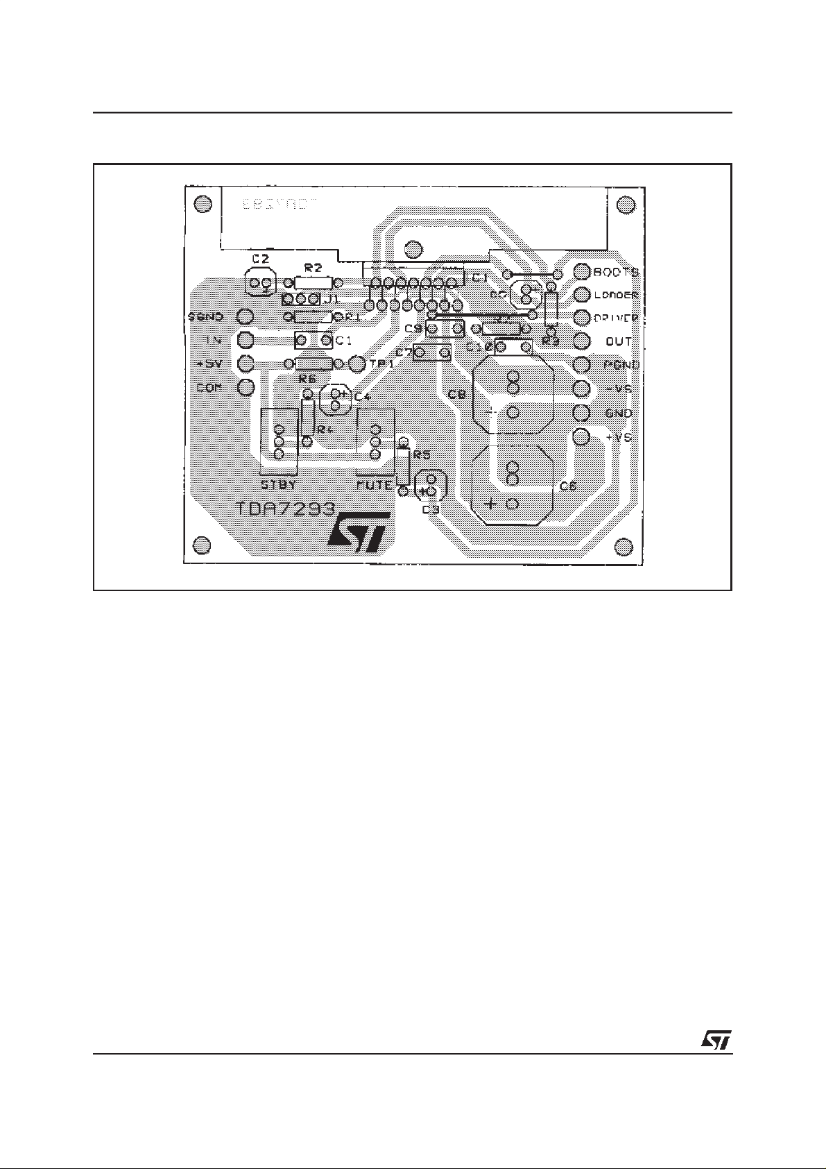
Figure 2: Typical Application P.C. Boardand ComponentLayout (scale1:1)
4/13

TDA7293
APPLICATIONSUGGESTIONS(seeTest andApplication Circuitsof the Fig. 1)
The recommendedvalues of the external components are those shown on the application circuit of Figure 1. Different valuescan be used; the followingtable can help the designer.
COMPONENTS SUGGESTED VALUE PURPOSE
LARGER THAN
SUGGESTED
R1 (*) 22k INPUT RESISTANCE INCREASE INPUT
IMPEDANCE
R2 680
Ω
CLOSED LOOP GAIN
DECREASE OF GAIN INCREASE OF GAIN
SMALLER THAN
SUGGESTED
DECREASE INPUT
IMPEDANCE
SET TO 30dB (**)
R3 (*) 22k INCREASE OF GAIN DECREASE OF GAIN
R4 22k ST-BY TIME
CONSTANT
LARGER ST-BY
ON/OFF TIME
SMALLER ST-BY
ON/OFF TIME;
POP NOISE
R5 10k MUTE TIME
CONSTANT
C1 0.47µF INPUT DC
DECOUPLING
LARGER MUTE
ON/OFF TIME
SMALLER MUTE
ON/OFF TIME
HIGHER LOW
FREQUENCY
CUTOFF
C2 22µF FEEDBACK DC
DECOUPLING
HIGHER LOW
FREQUENCY
CUTOFF
C3 10µF MUTE TIME
CONSTANT
C4 10µF ST-BY TIME
CONSTANT
LARGER MUTE
ON/OFF TIME
LARGER ST-BY
ON/OFF TIME
SMALLER MUTE
ON/OFF TIME
SMALLER ST-BY
ON/OFF TIME;
POP NOISE
C5 22µFXN (***) BOOTSTRAPPING SIGNAL
C6, C8 1000µF SUPPLY VOLTAGE
C7, C9 0.1µF SUPPLY VOLTAGE
(*) R1 = R3 for pop optimization
(**) Closed Loop Gain has to be≥26dB
(***) Multiplay this value for thenumber of modular part connected
Slave function:pin 4 (Ref to pin8 -VS)
+3V
-V
S
+1V
-V
S
-V
S
MASTER
UNDEFINED
SLAVE
D98AU821
DEGRADATION AT
LOW FREQUENCY
BYPASS
DANGER OF
BYPASS
OSCILLATION
Note:
If in the application, the speakers are connected
via long wires, it is a good rule to add between
the output and GND, a BoucherotCell, in order to
avoid dangerous spurious oscillations when the
speakersterminal are shorted.
The suggested Boucherot Resistor is 3.9Ω/2W
and the capacitoris 1µF.
5/13
 Loading...