

Page 1
CONTROL CIRCUIT FOR SWITCH MODE
1
2
3
4
8
7
6
5
REGULATION INPUT
PRIMARY CURRENT SIMULATION
PRIMARY VOLTAGE MONITORING
GROUND OUTPUT
SUPPLY VOLTAGE
SOFT-START
ZERO CROSSING DETECTOR INPUT
Obsolete Product(s) - Obsolete Product(s)
POWER SUPPLIES USING MOS TRANSISTORS
■ Fold-Back Characteristic provides Overload
Protection for External Diodes
■ Burst Operation under Short-Circuit and no
Load Conditions
■ Loop Error Protection
■ Switch-off in case of too low Line Voltage
(Under Voltage Switch-off)
■ Line Voltage Compensation of Overlo ad Point
■ Soft-Start for smooth Start-up
■ Chip Over-Temperature Protection (Thermal
Shutdown)
■ On-Chip Parasitic Transformer Oscillation
Suppression Circuitry
■ Decrease of Regulated Vol tage for low Power
Consumption
DESCRIPTION
The IC TDA4605 controls the MOS Power Transistor and performs all necessary regulation and
monitoring functions in free running flyback converters. Since good load regulation over a wide
load range is attained, this IC is particularly suitable for Consumer as well as Industrial Power Supplies.
Alternative source of the TDA 4605 is als o available from SIEMENS Semiconductors Consumer
Electronics A.G.
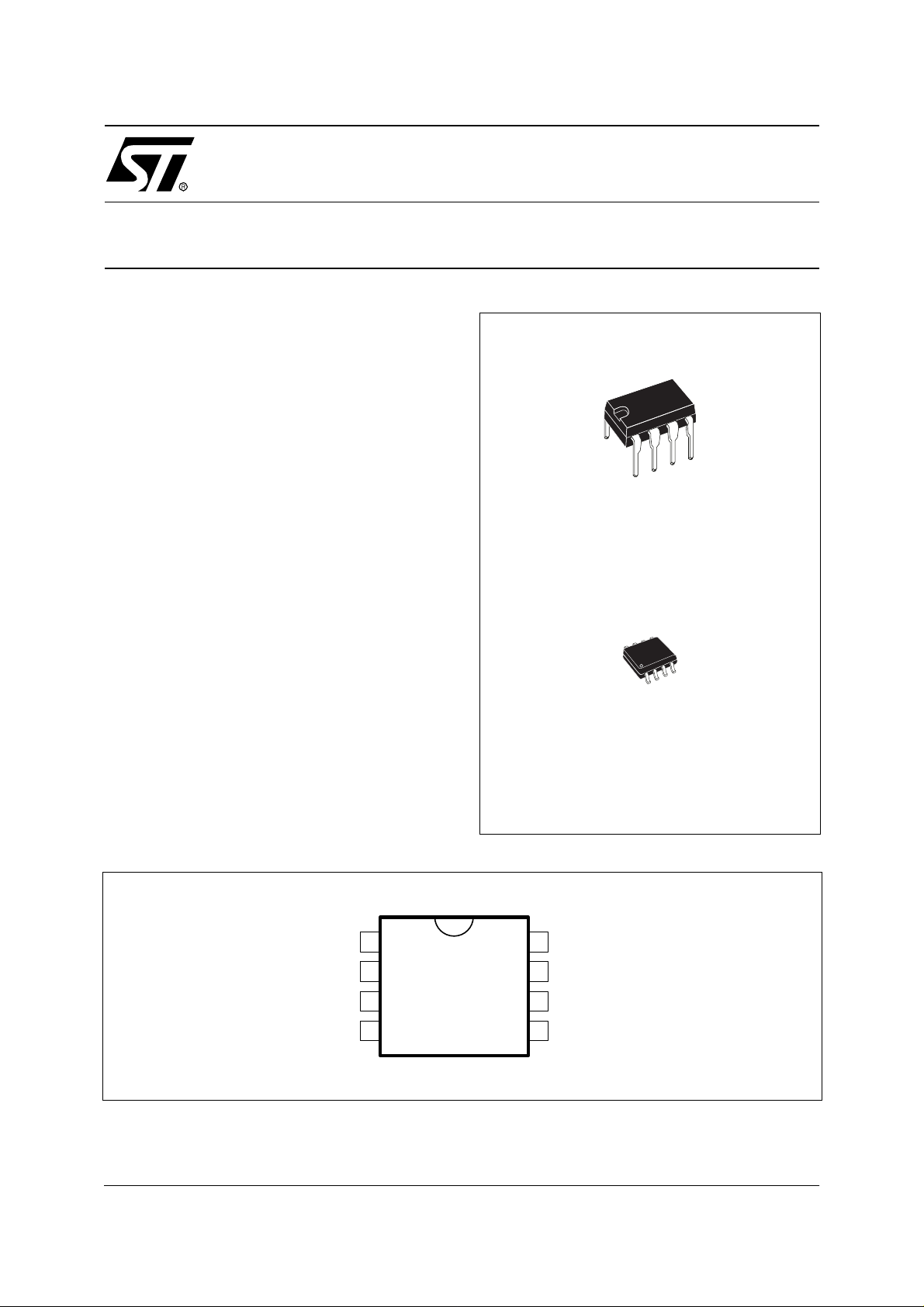
TDA4605
DIP28
(Plastic Package)
ORDER CODE: TDA4605
SO8
(Plastic Micropackage)
ORDER CODE: TDA4605D
Figure 1. Pin Connections
4605-01.eps
September 2003 1/7
1
Page 2
Obsolete Product(s) - Obsolete Product(s)
TDA4605
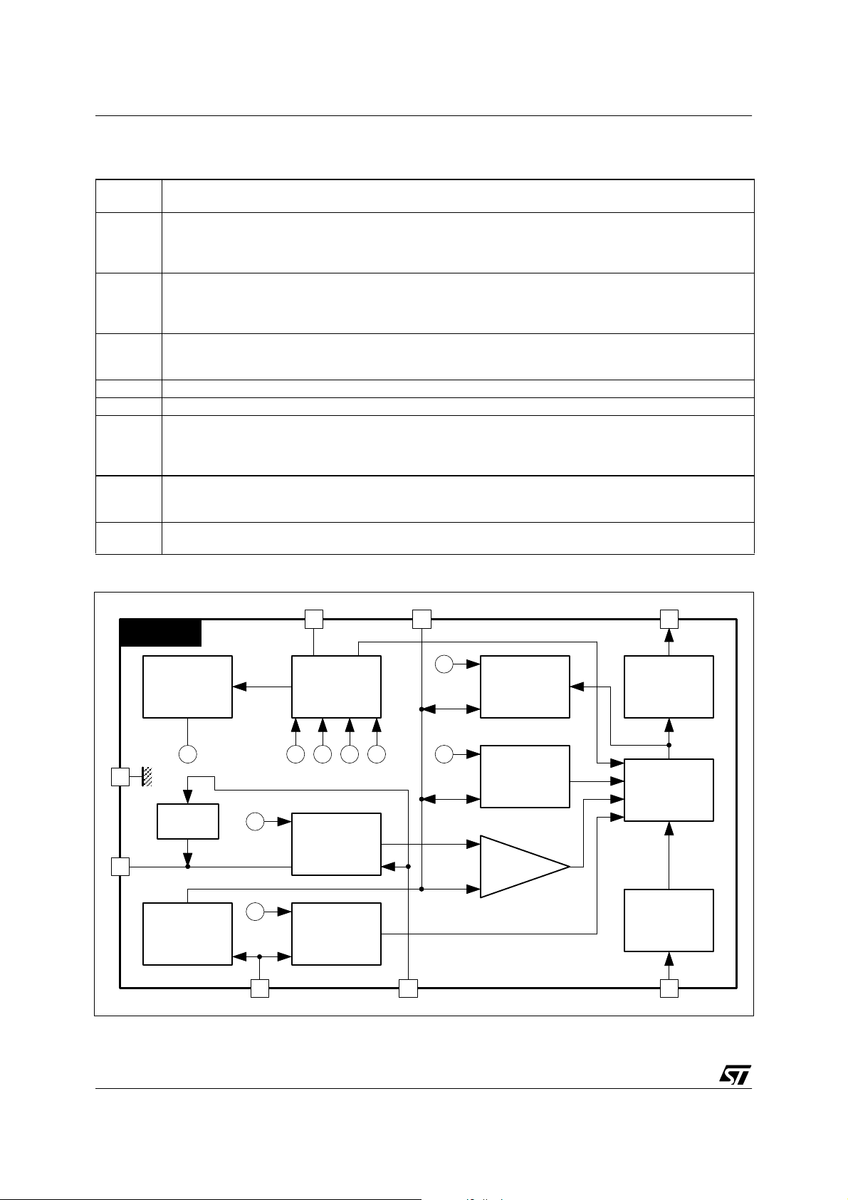
PIN CONFIGURATION
Pin
Number
Regulating voltage : information input concerning secondary voltage.
By comparing the regulating voltage obtained from the regulating winding of the transformer with the
1
internal reference voltage, the output pulse width on Pin 5 is adapted to the load of the secondary side
(normal, overload, short circuit, no load)
Primary current simulation : information input regarding the primary current. The primary current rise in the
primary winding is simulated at Pin 2 as a voltage rise by means of external RC element. When a value is
2
reached that is derived from the regulating voltage at Pin 1, the output pulse at Pin 5 is terminated. The RC
element serves to set the maximum power at the overload point.
Primary voltage detector : input for primary voltage monitoring. When the line voltage is too low the IC is
3
switched-off by comparing V
compensation.
4 Ground
5 Output : push-pull output for charge and discharge of the gate capacitance of the power MOS transistor.
Supply voltage : Supply voltage input. From it are derived a stable internal reference voltage (V
switching threshold V
6
if V
> V6E the V
6
min < V6 < V6 max.
V
6
Soft-start : input for soft-start and integration network. Start-up will begin with short pulses by connecting a
7
capacitor between Pin 7 to ground. This capacitor together with a resistor connected between Pin 7 and
error amplifier output also as acts an integrator network for regulation.
Zero detector : Input for the oscillator feedback. After starting oscillator, every zero transit of the feedback
8
voltage (falling edge) triggers an output pulse at Pin 5. The trigger threshold is at typically - 50mV
6A
is switched on and switched off when V6 < V6A. In addition the logic is only enable for
REF
with an internal reference. Voltage at Pin 3 is used for overload point
3
, V6E, V6 max and V6 min for the supply voltage detector.
Description
) and the
REF
Figure 2. Block Diagram
2
56
TDA4605
4
1
Reference
Voltage
(typ. 3V)
V
Current
Source
Overload
Point
Correction
REF
V
R
V
u
V
6min
Regulating
& Overload
Amplifier
Low Voltage
Protection
Monitoring
Supply
Voltage
Monitor
V
V
6A
6E
V
6max
V
2B
Primary
Current
Recopy
V
st
Starting
Impulse
Generator
Output Stage
and
Current Limit
Logic
Stop
Comp.
Zero
Crossing
Detector
3
7 8
4605-02.eps
2/7
1
Page 3
Obsolete Product(s) - Obsolete Product(s)
TDA4605
ABSOLUTE MAXIMUM RATINGS
Symbol Parameter Pin Value Unit
V
1
V
2
V
3
V
V
V
I
I
I
I
I
I
I
I
T
T
stg
Supply Voltage
4
6
7
1
2
3
t
50µs, V ≤ 0.1 4 - 1.5 A
4
Supply Current
5
6
7
8
Junction Temperature (autom. thermal disjunction) +125
j
≤
p
tp ≤ 50µs, V ≤ 0.1 5 -0.5, +1.5 A
tp ≤ 50µs, V ≤ 0.1 6 0.5 A
Storage Temperature -40, +125
THERMA L D ATA
Symbol Parameter Value Unit
R
(j-a) Junction-ambient Thermal Resistance 80
th
(j-c) Junction-case Thermal Resistance 45
R
th
T
amb
Ambient Temperature -20, +85
1 -0.3, +3 V
2 -0.3 V
3 -0.3 V
4 -0.3 V
6 -0.3, +20 V
7 -0.3 V
13mA
23mA
33mA
73mA
8 -3, +3 mA
o
C/W
o
C/W
o
o
C
o
C
C
ELECTRICAL CHARACTERISTICS
(V
= 10V, T
CC
= 25oC, unless otherwise specified)
amb
Symbol Parameter Test Conditions Min. Typ. Max. Unit
START-UP HYSTERESIS
I
6E0
V
V
I
6E1
I
6A1
VOLTAGE CLAMP (V
(Max.) At Pin 2 (V6 < V6E)I
V
2
V
(Max.) At Pin 3 (V6 < V6E)I
3
Start-up Current Drain V6 = V
Switch-on Voltage 11 12 13 V
6E
Switch-off Voltage 4.5 5 5.5 V
6A
Switch-on Current V6 = V
Switch-off Current V6 = V
= 10V, IC Switched off)
6
6E
6E
6A
= 1mA 5.6 6.6 9 V
2
= 1mA 5.6 6.6 9 V
3
0.6 0.8 mA
11 mA
10 mA
CONTROL RANGE
V
-V
Control Input Voltage 400 410 420 mV
1R
= d(V2S - V2B)/dV
V
Voltage Gain of the Control Circuit in the Control Range
R
R
f = 1kHz
1
43 dB
PRIMARY CURRENT SIMULATION VOLTAGE
V
Basic Value 0.955 1.00 1.03 V
2B
OVERLOAD RANGE AND SHORT CIRCUIT OPERATION
V
2O
DV
V
Peak Value in the Range of Secondary Overload V1 = V1R - 10mV 2.8 2.95 3.1 V
Maximum Ramp Amplitude V2O - V
2
Peak Value in the Range of Secondary Short
2S
Circuit Operation
2B
= 0 2.3 2.5 2.7 V
V
1
1.82 1.95 2.08 V
FOLDBACK POINT CORRECTION
-I
Foldback Point Correction Curre nt V3 = 3.7V 300 500 650 µA
2
3/7
1
Page 4

Obsolete Product(s) - Obsolete Product(s)
TDA4605
ELECTRICAL CHARACTERISTICS (V
= 10V, T
CC
= 25oC, unless otherwise specified) - Continued
amb
Symbol Parameter Test Conditions Min. Typ. Max. Unit
GENERALLY VALID DATA (V
VOLTAGE OF THE ZERO Transition DETECTOR
V
V
V
Positive Clamping Voltage I8 = 1mA 0.75 V
8P
Negative Clamping Voltage I8 = -1mA -0.2 V
8N
Threshold Value 40 50 mV
8S
= 10V)
6
TUL Suppression of Transformer Ringing 3 3.8 4.5 µs
-I
Input Current V8 = 0 0 4 µV
8
PUSH-PULL OUTPUT STAGE
SATURATION VOLTAGES
V
V
V
SatU
SatU
SatU
Pin 5 Sourcing I5 = -0.1A 1.5 2.0 V
Pin 5 Sinking I5 = 0.1A 1.0 1.2 V
Pin 5 Sinking I5 = 0.5A 1.4 1.8 V
OUTPUT SLOW RATE
/dt Rising Edge 70 V/µs
dV
5
/dt Falling Edge 100 V/µs
-dV
5
REDUCTION OF CONTROL VOLTAGE
-I
Current to reduce the Control Voltage V7 = 1V 50 µA
1
PROTECTION CIRCUIT
V
6
V
6
V
(Min.)
(Max.)
V
3A
Oj
3Sat
I
6
Undervoltage Protection for V
Voltage at Pin 5 = V
(Min.) if V6 < V6(Min.)
5
Overvoltage Protection for V
Voltage at Pin 5 = V
(Min.) if V6 > V6(Max.)
5
Undervoltage Protection for VAC :
Voltage at Pin 5 = V
(Min.) if V3 < V
5
Over Temperature : at the given chip temperature the
IC will switch V
to V5(Min.)
5
Voltage at Pin 3 if one of the protection functions was
triggered ; (V
will be clamped until V6 < V6A)
3
Current Drain during Burst Operation V3 = V2 = 0V 8 mA
:
6
:
6
3A
V2 = 0V 970 1005 1040 mV
7.0 7.25 7.5 V
15 16 16.5 V
150
= 750µA 0.4 0.8 V
I
3
o
C
4/7
1
Page 5

Obsolete Product(s) - Obsolete Product(s)
FUNCTIONAL DESCRIPTION
In free running fly-back converters, the TDA460 5
assumes control of a MOS power transistor and all
necessary regulation and monitoring functions.
The serial circuit of power transistor and primary
winding of the flyback transformer is co nnecte d to
the input voltage. During the switch-on period of
the transistor, energy is s tored in the tran sformer
and during the switch-off period it is fed to t he l oad
via the secondary winding. By varying the switchon time of the power transistor, the IC controls
each portion of energy transferred to the secondary side such that the output v oltage remains nearly independent of load variations.
The required control information is taken from th e
input voltage during the switch-on period and from
a regulation winding during the switch-off period. A
new cycle begins as soon as the energy stored in
the transformer has been totally delivered to the
secondary side.
TDA4605
In different load ranges, the SMPS will behave as
follows:
– No-Load Operation: The power supply unit os-
cillates in non continuous mode at a typical frequency of 20 to 40kHz. Depending upon the
transformer winding and the regulated voltage divider, the output voltage can be slightly above
the nominal value.
– Normal Operation: S tarting from typ. 200kHz,
the switching frequency falls with increasing load
and decreasing AC voltage. The duty cycle depends primarily on the AC voltage. The output
voltage is only slightly load-dependent.
– Overload Point: Maximum output po w er is
available at this point of the output characteristics
– Overload: The energy transferred per operation
cycle is limited at the top. Therefore, the output
voltage will fall with secondary overloading.
5/7
1
Page 6
Obsolete Product(s) - Obsolete Product(s)
TDA4605
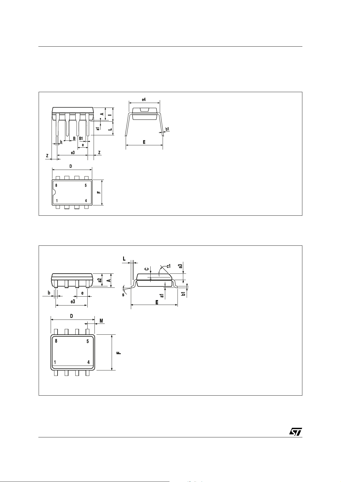
PACKAGE MECHANICAL DATA
8-PINS - PLASTIC DIP
Figure 3. 8-Pin Package
8-PINS - PLAS TI C SO
Figure 4. 8-Pin Plastic Micropackage
6/7
1
Page 7

Obsolete Product(s) - Obsolete Product(s)
TDA4605
Information furnished is believed to be accurate and reliable. However, STMicroelectronics assumes no responsibility for the consequences
of use of such information nor for any infringement of patents or other rights of third parties which may result from its use. No license is granted
by implic ation or otherwise under any patent or patent r i ght s of STMi croelectr oni cs. Spec i fications mentione d i n this publicatio n are subj ect
to change without notice. This publication supersedes and replaces all information previously supplied. STMicroelectronics product s are not
authorized for use as cri tical comp onents in lif e support devi ces or systems without the express written appr oval of STMic roelectronics.
The ST logo is a registered trademark of STMicroelectronics
2003 STMicroelectronics - All Rights Reserved.
Purchase of I
Australi a - Brazil - China - Finland - France - Germany - Hong Kong - India - Italy - Japan - Malaysia - Malt a - Mo rocco - Singa pore - Spain
2
C Components by STMicroelectronics conveys a license under the Philips I2C Patent. Rights to use the se components in an
2
C system i s granted pro vi ded that the sy stem conforms to the I2C Standard Specification as defined by Philips.
I
STMicroelectronics Grou p of Companies
Sweden - Switzerland - United K i ngdom - U.S.A.
http://www.s t. com
7/7
Page 8

 Loading...