STMicroelectronics TDA2050 Technical data

®
32W Hi-Fi AUDIO POWER AMPLIFIER
HIGH OUTPUT POWER
(50W MUSIC POWER IEC 268.3 RULES)
HIGH OPERATING SUPPLY VOLTAGE (50V)
SINGLE OR SPLIT SUPPLY OPERATIONS
VERY LOW DISTORTION
SHORT CIRCUIT PROTECTION (OUT TO
GND)
THERMAL SHUTDOWN
TDA2050
Pentawatt
DESCRIPTION
The TDA 2050 is a monolithic inte grated circuit in
Pentawatt package, intended for use as an audio
class AB audio amplifier. Thanks to its high power
capability the TDA2050 is able to provide up to
35W true rms power into 4 ohm load @ THD =
10%, V
= ±18V, f = 1KHz and up to 32W into
S
8ohm load @ THD = 10%, VS = ±22V, f = 1KHz.
Moreover, the TDA 2050 delivers typically 50W
music power into 4 ohm load over 1 sec at V
S
22.5V, f = 1KHz.
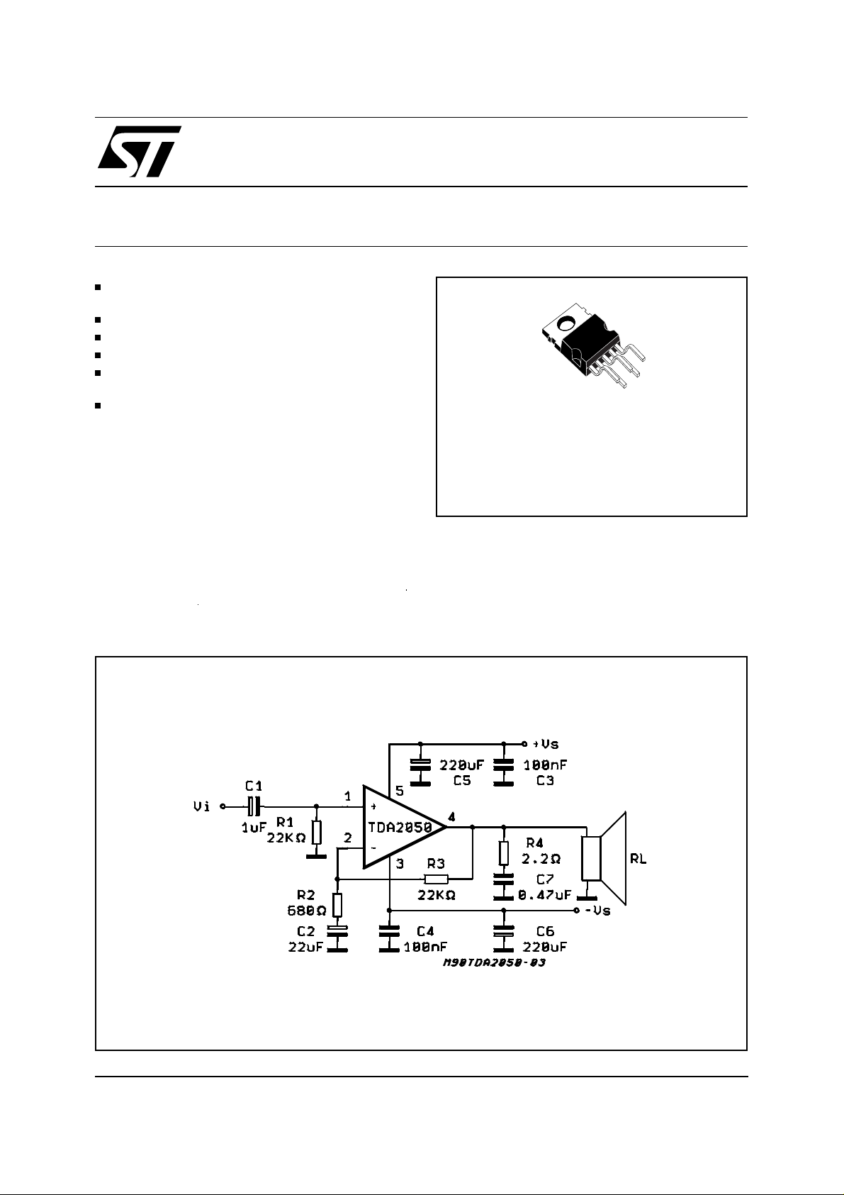
TEST AND APPLICATION CIRCUIT
ORDERING NUMBERS:
TDA2050H
TDA2050V
The high power and very low harmonic and crossover distortion (THD = 0.05% typ, @ VS = ±22V,
= 0.1 to 15W, RL=8ohm, f = 100Hz to 15KHz)
P
O
make the device most suitable for both HiFi and
=
high class TV sets.
March 2002
This is advanced information on a new product now in development or undergoing evaluation. Details are subject to change without notice.
1/13

TDA2050
ABSOLUTE MAXIMUM RATINGS
Symbol Parameter Value Unit
V
V
V
I
P
T
stg
Supply Voltage ±25 V
S
Input Voltage V
i
Differential Input Voltage ±15 V
i
Output Peak Current (internally limited) 5 A
O
Power Dissipation T
tot
= 75°C25W
CASE
S
, TjStorage and Junction Temperature -40 to 150 °C
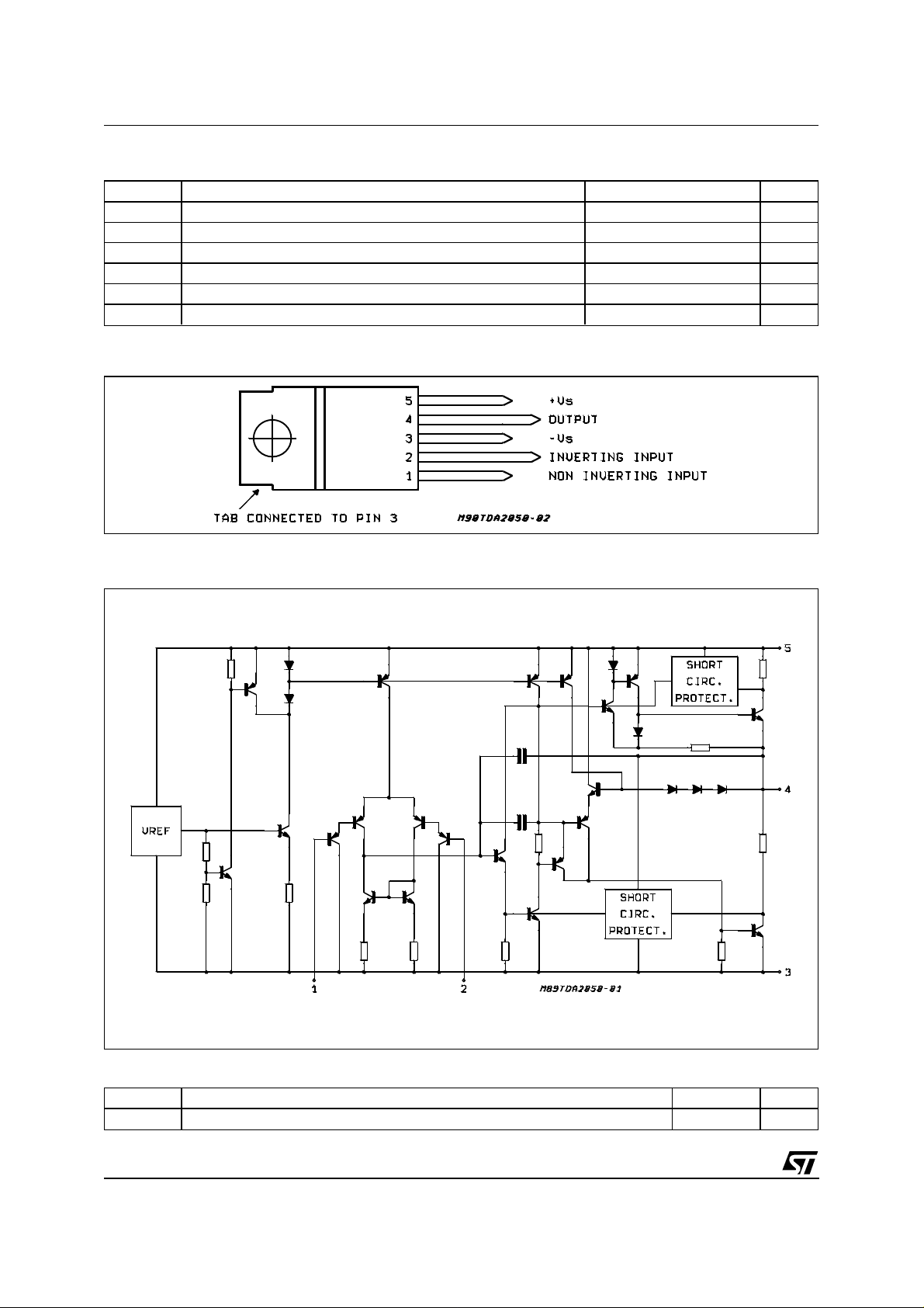
PIN CONNECTION
(Top view)
SCHEMATIC DIAGRAM
THERMAL DATA
Symbol Description Value Unit
Thermal Resistance junction-case Max 3 °C/W
2/13
R
th j-case

TDA2050
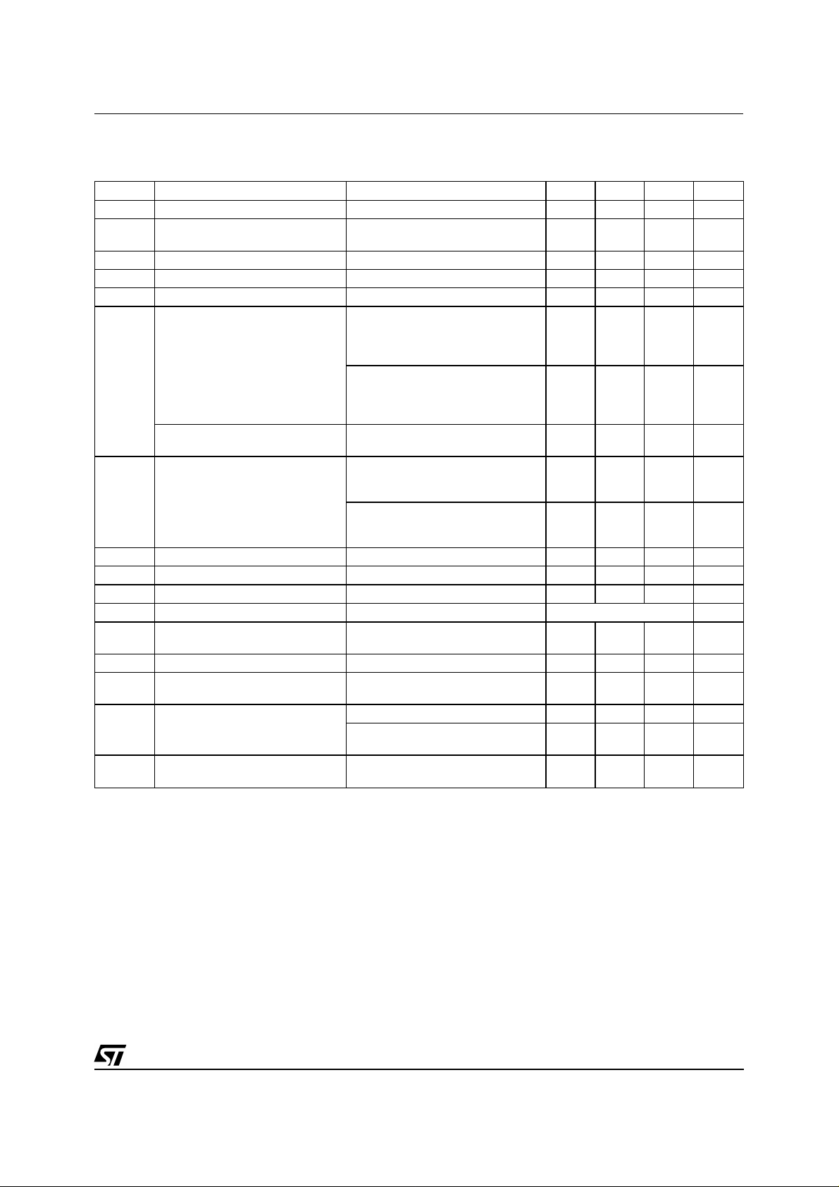
ELECTRICAL CHARACTERISTICS
(Refer to the Test Circuit, V
= ±18V, T
S
= 25°C, f = 1 kHz; un-
amb
less otherwise specified)
Symbol Parameter Test Condition Min. Typ. Max. Unit
V
I
I
V
I
OS
P
d Total Harmonic Distortion R
SR Slew Rate 5 8 V/µs
G
G
BW Power Bandwidth (-3dB) R
e
R
SVR Supply Voltage Rejection R
η Efficiency P
T
sd-j
Supply Voltage Range ±4.5 ±25 V
S
Quiescent Drain Current VS = ±4.5V
d
Input Bias Current VS = ±22V 0.1 0.5 µA
b
Input Offset Voltage VS = ±22V ±15 mV
OS
V
= ±25V
S
30
55
Input Offset Current VS = ±22V ±200 nA
RMS Output Power d = 0.5%
O
R
= 4Ω
L
R
= 8Ω
L
V
= ±22V RL = 8Ω
S
24
22
28
18
25
d = 10%
R
= 4Ω
L
R
= 8Ω
L
V
= ±22V RL = 8Ω
S
Music Power
IEC268.3 RULES
Open Loop Voltage Gain 80 dB
V
Closed Loop Voltage Gain 30 30.5 31 dB
V
Total Input Noise curve A
N
d = 10%; T = 1s
V
= ±22.5V; RL = 4Ω 50 W
S
= 4Ω
L
f = 1kHz, P
f = 100H z to 10 kHz, P
= ±22V RL = 8Ω
V
S
f = 1kHz, P
f = 100H z to 10 kHz, P
= 4Ω Vi = 200mV 20 to 80,000 Hz
L
= 0.1 to 24W
O
= 0.1 to 20W
O
O
O
= 0.1 to 18 W
= 0.1 to 15 W
B = 22Hz to 22kHz
Input Resistance (pin 1) 500 kΩ
i
= 22kΩ; f = 100Hz;
s
V
= 0.5Vrms 45 dB
ripple
= 28W; RL = 4Ω 65 %
O
35
22
32
0.03 0.5
0.02
4
510
PO = 25W; RL = 8Ω;
V
= ±22V 67 %
S
Thermal Shut-down
150 °C
Junction Temperature
50
90
0.5
0.5
mA
mA
W
W
W
W
W
W
%
%
%
%
µV
µV
3/13

TDA2050
Figure 1:
Figure 2:
Split Supply Typical Application Circuit
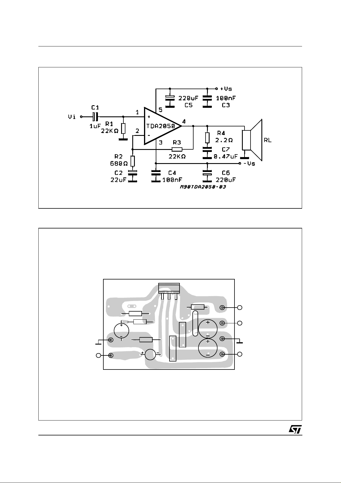
P.C. Board and Components Layout of the Circuit of Fig. 1 (1:1)
4/13
TDA2050
L
R4
R3
R2
C2
R1
C4
C1
Vi
C7
C5
C3
C6
R
+Vs
-Vs
 Loading...