

Page 1
■ 1A sink / 0.75A source min. gate drive
P
■ Active Miller clamp feature
■ Desaturation detection
■ Adjustable and accurate turn-on delay
■ UVLO protection
■ 2kV ESD protection
Description
TD352 is an advanced gate driver for IGBT and
power MOSFET. Control and protection functions
are included and allow the design of high reliability
systems.
Innovative active Miller clamp function avoids the
need of negative gate drive in most applications
and allows the use of a simple bootstrap supply
for the high side driver.
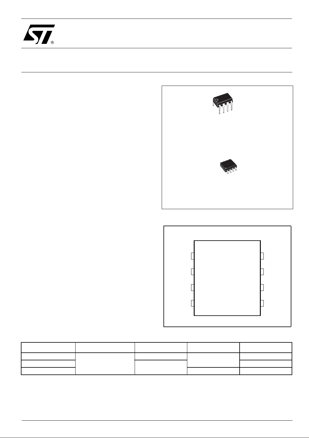
TD352
Advanced IGBT/MOSFET Driver
N
DIP-8
(Plastic Package)
D
SO-8
(Plastic Micropackage)
TD352 includes an adjustable turn-on delay. This
Pin Connections (top view)
feature can be used to implement reliable
deadtime between high and low sides of a half
bridge. External resistor and capacitor are used to
provide accurate timing.
Applications
■ 1200V 3-phase inverter
■ Motor control systems
■ UPS
VREF
TD352
CD VL
DESAT
Order Codes
Part Number Temperature Range Package Packaging Marking
TD352IN
TD352ID
TD352IDT Tape & Reel TD352I
-40°C, +125°C
DIP
SO
Tube
VHIN
OUT
CLAM
TD352I
TD352I
December 2004 Revision 1 1/13
Page 2
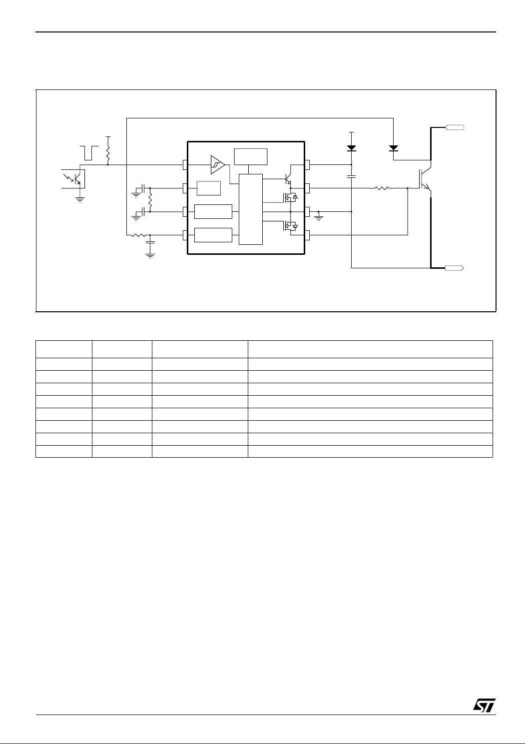
TD352 Block Diagram
1 Block Diagram
Figure 1. System and internal block diagram
VH
4.7k
IN VH
VREF
CD
DESAT
Vref
Delay
Desat
UVLO
OUT
VL
Control Block
CLAMP
16V
TD352
Table 1. Pin Description
Name Pin Number Type Function
IN 1 Analog input Input
VREF 2 Analog output +5V reference voltage
CD 3 Timing capacitor Turn on delay
DESAT 4 Analog input Desaturation protection
CLAMP 5 Analog output Miller clamp
VL 6 Power supply Signal ground
OUT 7 Analog output Gate drive output
VH 8 Power supply Positive supply
2/13
Page 3

Absolute Maximum Ratings TD352
2 Absolute Maximum Ratings
Table 2. Key parameters and their absolute maximum ratings
Symbol Parameter Value Unit
VHL Maximum Supply Voltage (VH - VL) 28 V
Vout Voltage on OUT, CLAMP, LVOFF pins VL-0.3 to VH+0.3 V
Vter Voltage on other pins (IN, CD, VREF) -0.3 to 7 V
Pd Power dissipation 500 mW
Tstg Storage temperature -55 to 150 °C
Tj Maximum Junction Temperature 150 °C
Rhja Thermal Resistance Junction-Ambient 150 °C/W
ESD Electrostatic discharge 2 kV
Table 3. Operating Conditions
Symbol Parameter Value Unit
VH Positive Supply Voltage vs. VL UVLO to 26 V
Toper Operating Free Air Temperature Range -40 to 125 °C
3/13
Page 4
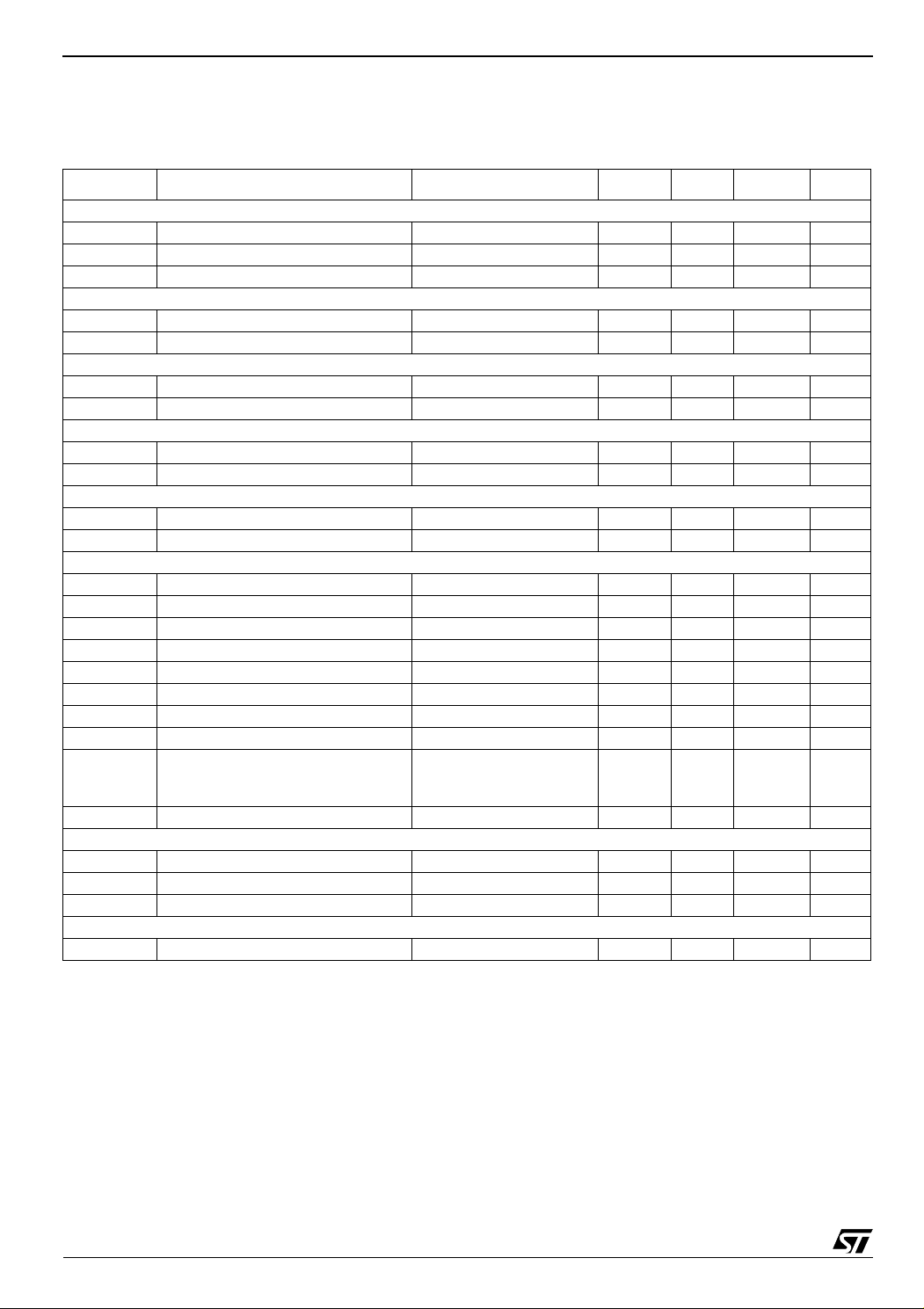
TD352 Electrical Characteristics
3 Electrical Characteristics
Table 4. T
Symbol Parameter Test Condition Min Typ Max Unit
Input
Vton IN turn-on threshold voltage 0.8 1.0 V
Vtoff IN turn-off threshold voltage 4.0 4.2 V
Iinp IN Input current IN input voltage < 4.5V 1
Voltage reference - Note 1
Vref Voltage reference T=25°C 4.85 5.00 5.15 V
Iref Maximum output current 10 mA
Clamp
Vtclamp CLAMP pin voltage threshold 2.0 V
VCL Clamp low voltage Icsink=500mA 2.5 V
Delay
Vtdel Voltage threshold 2.5 V
Rdel Discharge resistor I=1mA 500
Desaturation protection
Vdes Desaturation threshold VH-2
Ides Source current 250 µA
Outputs
Isink Output sink current Vout=6V 1000 1700 mA
Isrc Output source current Vout=VH-6V 750 1300 mA
VOL1 Output low voltage 1 Iosink=20mA 0.35 V
VOL2 Output low voltage 2 Iosink=500mA 2.5 V
VOH1 Output high voltage 1 Iosource=20mA VH-2.5 V
VOH2 Output high voltage 2 Iosource=500mA VH-4.0 V
tr Rise time CL=1nF, 10% to 90% 100 ns
tf Fall time CL=1nF, 90% to 10% 100 ns
tdon Turn on propagation delay
tdoff Turn off propagation delay 10% output change 400 ns
Under Voltage Lockout (UVLO)
UVLOH UVLO top threshold 10 11 12 V
UVLOL UVLO bottom threshold 9 10 11 V
Vhyst UVLO hysteresis Vhyst=UVLOH-UVLOL 0.5 1 V
Supply current
Iin Quiescent current input low, no load 2.5 mA
= -20 to 125°C, VH=16V (unless otherwise specified)
amb
10% output change:
Rd=4.7k, no Cd
Rd=11k, Cd=220pF 1.8 2.0
500
2.2
µA
Ω
ς
ns
µs
Note:1.Recommended capacitor range on VREF pin is 10nF to 100nF
4/13
Page 5

Functional Description TD352
4 Functional Description
4.1 Input stage
TD352 IN input is clamped at about 5V to 7V. The input is triggered by the signal edge. When using an
open collector optocoupler, the resistive pull-up resistor can be connected to either VREF or VH.
Recommended pull-up resistor value with VH=16V are from 4.7k to 22k.
4.2 Voltage reference
A voltage reference is used to create accurate timing for the turn-on delay with external resistor and
capacitor. The same circuitry is also used for the two-level turn-off delay.
A decoupling capacitor (10nF to 100nF) on VREF pin is required to ensure good noise rejection.
4.3 Active Miller clamp:
The TD352 offers an alternative solution to the problem of the Miller current in IGBT switching
applications. Instead of driving the IGBT gate to a negative voltage to increase the safety margin, the
TD352 uses a dedicated CLAMP pin to control the Miller current. When the IGBT is off, a low impedance
path is established between IGBT gate and emitter to carry the Miller current, and the voltage spike on
the IGBT gate is greatly reduced.
During turn-off, the gate voltage is monitored and the clamp output is activated when gate voltage goes
below 2V (relative to VL). The clamp voltage is VL+4V max for a Miller current up to 500mA. The clamp
is disabled when the IN input is triggered again.
The CLAMP function doesn’t affect the turn-off characteristic, but only keeps the gate to the low level
throughout the off time. The main benefit is that negative voltage can be avoided in many cases, allowing
a bootstrap technique for the high side driver supply.
4.4 Turn-on delay
Turn-on (Ta) delay is programmable through external resistor Rd and capacitor Cd for accurate timing. T
is approximately given by:
T
(µs) = 0.7 * Rd (kohms) * Cd (nF)
a
The turn-on delay can be disabled by connecting the CD pin to VREF with a 4.7k resistor.
Input signals with ON-time smaller than T
are ignored.
a
4.5 Desaturation protection
Desaturation protection ensures the protection of the IGBT in the event of overcurrent. When the DESAT
voltage goes higher than VH-2V, the TD352 OUT pin is driven low. The fault state is only exit after powerdown and power-up.
A programmable blanking time is used to allow enough time for IGBT saturation. Blanking time is
provided by an internal current source and external C
capacitor, the T
des
blanking time value is given
bdes
by:
= V
T
bdes
At VH=16V, T
(µs) = 0.056 * C
T
bdes
des
* C
/ I
des
des
is approximately given by:
bdes
des
(pF)
4.6 Output stage
The output stage is able to sink/source 1.7A/1.3A typical at 25°C and 1.0A/0.75A min. over the full
temperature range. This current capability is specified near the usual IGBT Miller plateau.
a
5/13
Page 6

TD352 Functional Description
4.7 Undervoltage protection
Undervoltage detection protects the application in the event of a low VH supply voltage (during start-up or
a fault situation). During undervoltage, the OUT pin is driven low (active pull-down for VH>2V, passive
pull-down for VH<2V.
Figure 2. Undervoltage protection
UVH
UVL
VH
Vccmin
OUT
FAULT
2V
6/13
Page 7

Functional Description TD352
Figure 3. Detailed internal schematic
UVLO
IN
VREF
D
ESAT
Comp_Input
7V
1V-4V
5V Vref
Comp_DelayOff
2.5V
S2
VH
250uA
Comp_Desat
VH-2V
S1
Control Block
Comp_Clamp
CLAMP
2V
VH
OUT
VL
rev. 2
7/13
Page 8

TD352 Timing Diagrams
5 Timing Diagrams
Figure 4. General turn-on and turn-off sequence
IN
CD
OUT
CLAMP
Vge
Vce
Ta
VL level
Twin
VH level
Twout
Open
VH level
Miller plateau
Figure 5. input and output waveform dynamic parameters
Twin
IN
(level mode)
IN
(edge mode)
Vton
VL level
Clamp threshold
Vtoff
Vtoff
OUT
Figure 6. Desaturation fault
IN
CD
OUT
DESAT
8/13
tdon
Vton
VH level
Twout
2.5V
Ta
VH-2V
Desat Blanking Time
tdoff
VH level
VL level
VL level
Page 9

Typical Performance Curves TD352
6 Typical Performance Curves
Figure 7. Quiescent current vs. temperature Figure 8. Low level output voltage vs.
temperature
2.5
2.0
1.5
In (mA)
1.0
0.5
0.0
- 50 -25 0 25 50 75 100 125
Temp (°C)
3.0
3.0
2.0
2.0
Iosink=500mA
Iosink=500mA
VOL -VL ( V)
VOL -VL ( V)
1.0
1.0
Iosink=20mA
Iosink=20mA
0.0
0.0
-50 -25 0 25 50 75 100 125
-50 -25 0 25 50 75 100 125
Temp (°C)
Temp (°C)
Figure 9. Sink current vs. temperature Figure 10. Rdel resistance vs. temperature
Isink (mA)
2000
1800
1600
1400
1200
500
400
300
200
Rdel (Ohms)
100
1000
-50 - 25 0 25 50 75 100 125
Temp (°C)
Figure 11. High level output voltage vs.
temperature
4.0
4.0
3.0
3.0
Iosource=500mA
Iosource=500mA
2.0
2.0
VH- VOH (V)
VH- VOH (V)
1.0
1.0
0.0
0.0
-50 -25 0 25 50 75 100 125
-50 -25 0 25 50 75 100 125
Temp (°C)
Temp (°C)
Iosource=20mA
Iosource=20mA
0
-50-250 255075100125
Temp (°C)
Figure 12. Source current vs. temperature
1600
1400
1200
Isrc (mA)
1000
800
-50 -25 0 25 50 75 100 125
Temp (°C)
9/13
Page 10

TD352 Application Diagrams
7 Application Diagrams
Figure 13. Single supply IGBT drive with active Miller clamp
VH
4.7k
IN VH
VREF
CD
DESAT
Vref
Delay
Desat
UVLO
Control Block
OUT
VL
CLAMP
TD352
Figure 14. Use of DESAT input for direct overcurrent detection
VH
Vref
4.7k
IN VH
VREF
CD
Vref
Delay
UVLO
OUT
VL
16V
16V
DESAT
Desat
Control Block
CLAMP
TD352
Figure 15. Large IGBT drive with negative voltage gate drive and optional current buffers
VH
16V
-10V
4.7k
IN VH
VREF
DESAT
CD
Vref
Delay
Desat
UVLO
Optional
OUT
VL
Control Block
TD352
CLAMP
Optional
10/13
Page 11

Package Mechanical Data TD352
8 Package Mechanical Data
8.1 DIP-8 Package
Plastic DIP-8 MECHANICAL DATA
DIM.
A 3.3 0.130
a1 0.7 0.028
B 1.39 1.65 0.055 0.065
B1 0.91 1.04 0.036 0.041
b 0.5 0.020
b1 0.38 0.5 0.015 0.020
D 9.8 0.386
E 8.8 0.346
e 2.54 0.100
e3 7.62 0.300
e4 7.62 0.300
F 7.1 0.280
I 4.8 0.189
L 3.3 0.130
Z 0.44 1.6 0.017 0.063
MIN. TYP MAX. MIN. TYP. MAX.
mm. inch
P001F
11/13
Page 12

TD352 Package Mechanical Data
8.2 SO-8 Package
SO-8 MECHANICAL DATA
DIM.
A 1.35 1.75 0.053 0.069
A1 0.10 0.25 0.04 0.010
A2 1.10 1.65 0.043 0.065
B 0.33 0.51 0.013 0.020
C 0.19 0.25 0.007 0.010
D 4.80 5.00 0.189 0.197
E 3.80 4.00 0.150 0.157
e 1.27 0.050
H 5.80 6.20 0.228 0.244
h 0.25 0.50 0.010 0.020
L 0.40 1.27 0.016 0.050
k ˚ (max.)
ddd 0.1 0.04
MIN. TYP MAX. MIN. TYP. MAX.
mm. inch
8
12/13
0016023/C
Page 13

Revision History TD352
9 Revision History
Date Revision Description of Changes
01 Dec. 2004 1 First Release
Information furnished is believed to be accurate and reliable. However, STMicroelectronics assumes no responsibility for the consequences
of use of such information nor for any infringement of patents or other rights of third parties which may result from its use. No license is granted
by implication or otherwise under any patent or patent rights of STMicroelectronics. Specifications mentioned in this publication are subject
to change without notice. This publication supersedes and replaces all information previously supplied. STMicroelectronics products are not
authorized for use as critical components in life support devices or systems without express written approval of STMicroelectronics.
The ST logo is a registered trademark of STMicroelectronics
All other names are the property of their respective owners
© 2004 STMicroelectronics - All rights reserved
Australia - Belgium - Brazil - Canada - China - Czech Repubic - Finland - France - Germany - Hong Kong - India - Israel - Italy - Japan -
Malaysia - Malta - Morocco - Singapore - Spain - Sweden - Switzerland - United Kingdom - United States of America
STMicroelectronics group of companies
www.st.com
13/13
 Loading...