

TD350
Advanced IGBT/MOSFET Driver
■ 0.75A source/1.2A sink min gate drive
■ Active Miller clamp feature
■ Two steps turn-off with adjustable level
and delay
■ Desaturation detection
■ Fault status output
■ Negative gate drive ability
■ Input compatible with pulse transformer or
optocoupler
■ Separate sink and source outputs for easy
gate dr i ve
■ UVLO protection
■ 2kV ESD protection
Description
TD350 is an advanced gate driver for IGBT and
power MOSFET. Control and protection functions
are included and allow the design of high reliability
systems.
Innovative active Miller clamp function avoids the
need of negative gate drive in most applications
and allows th e use of a simple bo otstrap supply
for the high side driver
TD350 includes a two-level turn-off feature with
adjustable level and delay. This function protects
against excessive overvoltag e at turn-off in case
of overcurrent or short-circuit condition. Same
delay is applied at turn-on to prevent pulse width
distortion.
TD350 also includes an IGBT desaturation
protection and a FAULT status output.
TD350 is compat ible with both pulse transformer
and optocoupler signals.
Applications
■ 1200V 3-Phase Inverter
■ Motor C
ontrol
■ UPS Systems
D
SO-14
(Plastic MicroPacka ge)
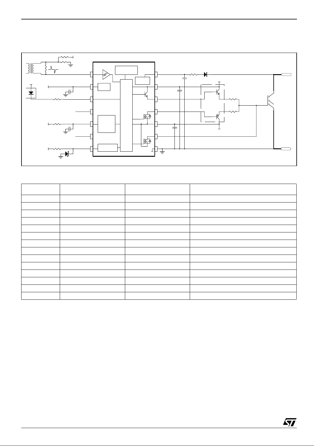
Pin Connections (top view )
1
IN
VREF
FAULT
NC
COFF
NC
LVOFF
2
3
4
5
6
7
TD350
14
11
13
12
10
DESAT
VH
OUTH
OUTL
VL
9
CLAMP
8
GND
Order Codes
Part Number Temperature Range Package Packaging
TD350ID
TD350IDT Tape & Reel
August 2004 Revision 1 1/11
-40, +125°C SO
Tube
TD350 Block Diagram
1 Block Diagram
Figure 1: Sche m atic block diagram
Vref
Off
UVLO
DESAT
Desat
Control Block
VH
OUTH
OUTL
VL
CLAMP
GND
16V
Optionnal
-10V
Pulse Transformer
VH
Vref
Vref
VH
IN
VREF
FAULT
NC
COFF
NC
LVOFF
Vref
delay
Off Level
TD350
Table 1: Pin description
Name Pin Number Type Function
IN 1 Analog input Input
VREF 2 Analog output +5V reference voltage
FAULT 3 Digital output Fault status output
NC 4 Not connected
COFF 5 Timing capacitor Turn off delay
NC 6 Not connected
LVOFF 7 Analog input Turn off level
GND 8 Power supply Signal ground
CLAMP 9 Analog output Miller clamp
VL 10 Power supply Negative supply
OUTL 11 Analog output Gate drive output (sink)
OUTH 12 Analog output Gate drive output (source)
VH 13 Power supply Positive supply
DESAT 14 Analog input Desaturation protection
2/11
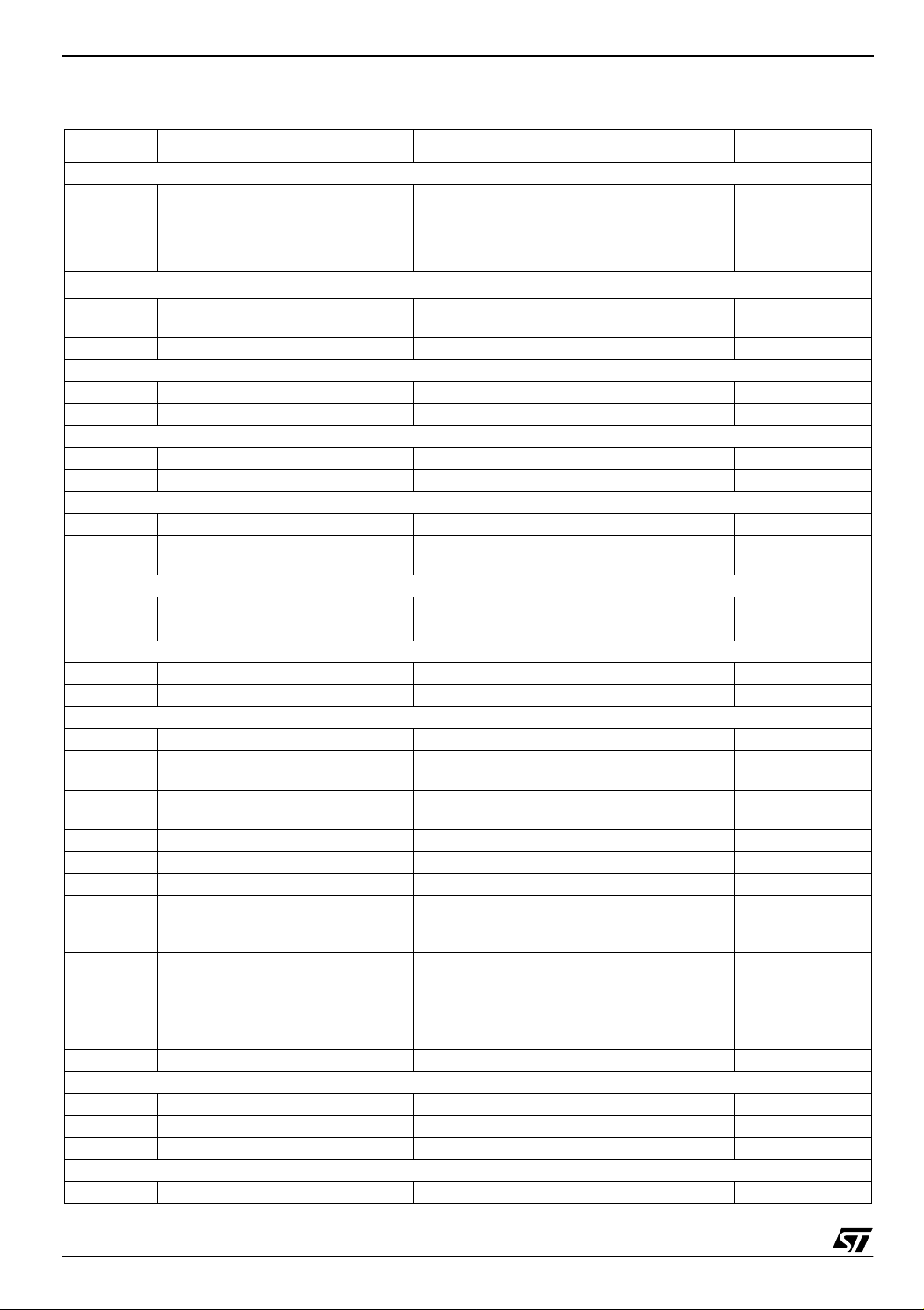
Absolute Maximum Ratin gs TD350
2 Absolute Maximum Rat ings
Table 2: Key parameters and their absolute maximum ratings
Symbol Parameter Value Unit
VHL Maximum Supply Voltage (VH - VL) 28 V
VH Maximum VH voltage vs. GND 28 V
VL Minimum VL voltage vs. GND -12 V
Vout Voltage on OUTH, OUTL, CLAMP pins VL-0.3 to VH+0.3 V
Vdes Voltage on DESAT, FAULT, LVOFF pin -0.3 to VH+0.3 V
Vter Voltage on other pins (IN, COFF, VREF) -0.3 to 7 V
Pd Power dissipation 500 mW
Tstg Storage temperature -55 to 150 °C
Tj Maximum Junction Temperature 150 °C
Rhja Thermal Resis tance Junction-A mbie nt 125 °C/W
Rhjc The rmal Resis tance Junction-C ase 22 °C/W
ESD Electrostatic discharge 2 kV
Table 3: Operat in g conditions
Symbol Parameter Value Unit
VH Positive Supply Voltage vs. GND UVLO to 26 V
VL Negative Supply Voltage vs. GND 0 to -10 V
VH-VL Maximum Total Supply Voltage 26 V
Toper Operating Free Air Temperature Range -40 to 125 °C
3/11
TD350 Electrical Characteristics
3 Electrical Characteristics
Table 4: T
Symbol Parameter Test Condi t io n Min Ty p Max Unit
Input
Vton IN turn-on threshold voltage 0.8 1.0 V
Vtoff IN turn-off threshold voltage 4.0 4.2 V
tonmin Minimum pulse width 100 135 220 ns
Iinp IN Input current 1
Voltage reference - note
Vref Voltage reference
Iref Maximum output current 10 mA
Desaturation protection
Vdes Desaturation threshold 6.5 7.2 7.9 V
Ides Source current 250
Fault output
tfault Delay for fault detection 500 ns
VFL FAULT low voltage Ifsink=10mA 1 V
Clamp
Vtclamp CLAMP pin voltage threshold 2.0 V
VCL Clamp low voltage at Icsink=500mA
Off Delay
Vtdel Voltage threshold 2.35 2.50 2.65 V
Rdel Disch arge resisto r I=1mA 500
Off Levels
Iblvoff LVOFF peak input current (sink) LVOFF=12V 120 200
Violv Offset voltage LVOFF=12V -0.3 -0.15 0 V
Outputs
VOL1 Output low voltage at Iosink=20mA VL+0.35 V
VOL2 Output low voltage at Iosink=200mA
VOL3 Output low voltage at Iosink=500mA
VOH1 Output high voltage 1 Iosource=20mA VH-2.5 V
VOH2 Output high voltage 2 Iosource=200mA VH-3.0 V
VOH3 Output high voltage 3 Iosource=500mA VH-4.0 V
tr Rise time
tf
tpd
∆tw Input to output pulse distortion 10% output change 10 60 110 ns
Under Voltage Lockout (UVLO)
UVLOH UVLO top threshold 10 11 12 V
UVLOL UVLO bottom threshold 9 10 11 V
Vhyst UVLO hysteresis UVH-UVL 0.5 1 V
Supply current
Iin Quiescent current output=0V, no load 5 mA
1) Recommended capac itor range on VR E F pi n i s 10nF to 100nF.
4/11
= -20 to 125°C, VH=16V, VL=-10V (unless otherwise spe cified)
amb
1
T=25°C
Tmin<T<Tmax
T=25°C
Tmin<T<Tmax
T=25°C
Tmin<T<Tmax
T=25°C
Tmin<T<Tmax
CL=1nF, 10% to 90%
VL=0
VL=-10V
Fall time
(2 step turn-off disabled)
Input to output propagation delay at
turn-on (2 step delay disabled)
CL=1nF, 90% to 10%
VL=0
VL=-10V
10% output change
4.85
4.77
270 800 ns
5.00 5.15
5.22
VL+2.5
VL+3.0
VL+1.0
VL+1.5
VL+2.5
VL+3.0
130
175
75
90
µA
V
V
µA
V
V
Ω
µA
V
V
V
V
ns
ns
ns
ns
 Loading...