

STMicroelectronics STP6NK90Z, STP6NK90ZFP, STB6NK90Z, STW7NK90Z Technical data
STP6NK90Z - STP6NK90ZFP
3
STB6NK90Z - STW7NK90Z
N-channel 900V - 1.56Ω - 5.8A - TO-220/TO-220FP/D2PA K/ TO -2 4 7
Zener-protected SuperMESH™ Power MOSFET
General features
V
Type
DSS
(@Tjmax)
R
DS(on)
I
D
STP6NK90Z 900 V < 2 Ω 5.8 A
STP6NK90ZFP 900 V < 2 Ω 5.8 A
STB6NK90Z 900 V < 2 Ω 5.8 A
STW7NK90Z 900 V < 2 Ω 5.8 A
■ Extremely high dv/dt capability
■ 100% avalange tested
■ Gate charge minimized
■ Very low intrinsic capacitances
■ Very good manufacturing repeatibility
Description
The SuperMESH™ series is obtained through an
extreme optimization of ST’s well established
strip-based PowerMESH™ layout. In addition to
pushing on-resistance significantly down, special
care is taken to ensure a very good dv/dt
capability for the most demanding applications.
Such series complements ST full range of high
voltage MOSFETs including revolutionary
MDmesh™ products.
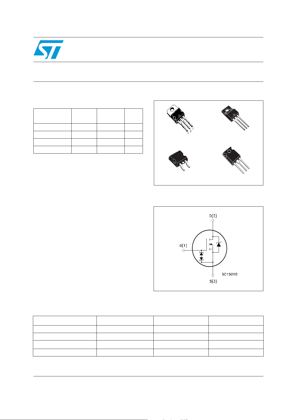
TO-220
D2PAK
3
1
TO-220FP
TO-247
Internal schematic diagram
2
1
Applications
■ Switching application
Order codes
Part number Marking Package Packaging
STP6NK90Z P6NK90Z TO-220 Tube
STP6NK90ZFP P6NK90ZFP TO-220FP Tube
STB6NK90ZT4 B6NK90Z
STW7NK90Z W7NK90Z TO-247 Tube
August 2006 Rev 4 1/18
2
PA K
D
Tape e reel
www.st.com
18

Contents STP6NK90Z - STP6NK90ZFP - STB6NK90Z - STW7NK90Z
Contents
1 Electrical ratings . . . . . . . . . . . . . . . . . . . . . . . . . . . . . . . . . . . . . . . . . . . . 3
1.1 Protection features of gate-to-source zener diodes . . . . . . . . . . . . . . . . . . 4
2 Electrical characteristics . . . . . . . . . . . . . . . . . . . . . . . . . . . . . . . . . . . . . 5
2.1 Electrical characteristics (curves) . . . . . . . . . . . . . . . . . . . . . . . . . . . . . 7
3 Test circuit . . . . . . . . . . . . . . . . . . . . . . . . . . . . . . . . . . . . . . . . . . . . . . . 10
4 Package mechanical data . . . . . . . . . . . . . . . . . . . . . . . . . . . . . . . . . . . . 11
5 Packaging mechanical data . . . . . . . . . . . . . . . . . . . . . . . . . . . . . . . . . . 16
6 Revision history . . . . . . . . . . . . . . . . . . . . . . . . . . . . . . . . . . . . . . . . . . . 17
2/18
STP6NK90Z - STP6NK90ZFP - STB6NK90Z - STW7NK90Z Electrical ratings
1 Electrical ratings
Table 1. Absolute maximum ratings
Symbol Parameter Value Unit
Drain-source voltage (VGS = 0) 900 V
DS
Gate-source voltage ± 30 V
GS
Drain current (continuous) at TC = 25°C 5.8 5.8
I
D
Drain current (continuous) at TC = 100°C 3.65 3.65
I
D
(2)
Drain current (pulsed) 23.2 23.2
Total dissipation at TC = 25°C 140 30 W
TOT
I
DM
P
V
V
Derating factor 1.12 0.24 W/°C
(3)
dv/dt
Peak diode recovery voltage slope 4.5 V/ns
Insulation withstand voltage (RMS) from
V
all three leads to external heat sink
ISO
(t=1s; Tc= 25°C)
Max operating junction temperature
T
j
T
1. Limited only by maximum temperature allowed
2. Pulse width limited by safe operating area
3. ISD ≤ 5.8 A, di/dt ≤ 200A/µs, VDD ≤ V
Storage temperature
stg
(BR)DSS
, Tj ≤ T
JMAX.
TO-220/
2
D
PA K/ TO2 47
TO220FP
- 2500 V
-55 to 150
(1)
(1)
(1)
A
A
A
°C
°C
Table 2. Thermal data
Symbol Parameter Value Unit
2
D
PAK
TO-220FP TO-247
0.39 4.2 0.89 °C/W
60 °C/W
62.5 50 °C/W
300 °C
R
thj-case
R
thj-pcb
R
thj-amb
Thermal resistance junctioncase max
Thermal resistance junctioncase max
Thermal resistance junctionambient max
Maximum lead temperature for
T
l
soldering purpose
TO-220
3/18

Electrical ratings STP6NK90Z - STP6NK90ZFP - STB6NK90Z - STW7NK90Z
Table 3. Avalanche characteristics
Symbol Parameter Value Unit
I
AR
E
Avalanche current, repetitive or not-repetitive
(pulse width limited by Tj Max)
Single pulse avalanche energy
AS
(starting Tj=25°C, Id=Iar, Vdd=50V)
5.8 A
300 mJ
Table 4. Gate-source zener diode
Symbol Parameter Test conditions Min. Typ. Max. Unit
BV
Gate-source breakdown voltage Igs=± 1mA (Open Drain) 30 V
GSO
1.1 Protection features of gate-to-source zener diodes
The built-in back-to-back Zener diodes have specifically been designed to enhance not only
the device’s ESD capability, but also to make them safely absorb possible voltage transients
that may occasionally be applied from gate to source. In this respect the Zener voltage is
appropriate to achieve an efficient and cost-effective intervention to protect the device’s
integrity. These integrated Zener diodes thus avoid the usage of external components.
4/18
STP6NK90Z - STP6NK90ZFP - STB6NK90Z - STW7NK90Z Electrical characteristics
2 Electrical characteristics
(T
=25°C unless otherwise specified)
CASE
Table 5. On/off states
Symbol Parameter Test conditions Min. Typ. Max. Unit
V
(BR)DSS
I
DSS
I
GSS
V
GS(th)
R
DS(on)
Drain-source
Breakdown voltage
Zero gate voltage
Drain current (V
GS
= 0)
Gate-body leakage
Current (V
DS
= 0)
Gate threshold voltage
Static drain-source on
resistance
=1mA, VGS = 0
I
D
= Max Rating
V
DS
= Max Rating, TC = 125°C
V
DS
VGS = ± 20 V
= VGS, ID = 100 µA
V
DS
VGS = 10 V, ID = 2.9 A
900 V
1
50µAµA
± 10 µA
33.754.5 V
1.56 2 Ω
Table 6. Dynamic
Symbol Parameter Test conditions Min. Typ. Max. Unit
g
C
oss eq.
(1)
fs
C
C
C
Forward transconductance
Input capacitance
iss
Output capacitance
oss
Reverse transfer capacitance
rss
(2)
Equivalent output
capacitance
= 15v, ID = 2.9 A
V
DS
= 25 V, f = 1 MHz,
V
DS
= 0
V
GS
VDS =0V, VDS = 0V to 720V
5S
1350
130
26
70 pF
pF
pF
pF
t
d(on)
t
r(off)
Q
Q
Q
T
r(Voff)
T
1. Pulsed: pulse duration=300µs, duty cycle 1.5%
2. C
increases from 0 to 80% V
Turn-on delay time
t
Rise time
r
Turn-off delay time
Fall time
t
r
g
Total gate charge
Gate-source charge
gs
Gate-drain charge
gd
Off-voltage rise time
T
Fall time
r
Cross-over time
c
is defined as a constant equivalent capacitance giving the same charging time as C
oss eq.
DSS
.
= 450 V, ID = 3 A,
V
DD
R
= 4.7 Ω, V
G
GS
(see Figure 20)
= 720 V, ID = 5.8 A,
V
DD
= 10 V
V
GS
= 720 V, ID = 5.8 A,
V
DD
= 4.7 Ω, V
R
G
GS
(see Figure 22)
= 10 V
= 10 V
17
45
20
20
46.5
8.5
25
11
12
20
60.5 nC
when VDS
oss
ns
ns
ns
ns
nC
nC
ns
ns
ns
5/18

Electrical characteristics STP6NK90Z - STP6NK90ZFP - STB6NK90Z - STW7NK90Z
Table 7. Source drain diode
Symbol Parameter Test conditions Min. Typ. Max. Unit
I
SD
I
SDM
V
SD
t
rr
Q
rr
I
RRM
1. Pulsed: pulse duration=300µs, duty cycle 1.5%
2. Pulse width limited by safe operating area
Source-drain current
(1)
Source-drain current (pulsed)
(2)
Forward on voltage
Reverse recovery time
Reverse recovery charge
Reverse recovery current
= 5.8 A, VGS = 0
I
SD
= 5.8 A, di/dt = 100
I
SD
A/µs
= 36 V, Tj = 150°C
V
DD
(see Figure 22)
840
5880
14
5.8
23.2AA
1.6 V
ns
µC
A
6/18
 Loading...