

Page 1
2.0-channel high-efficiency digital audio system
Features
■ Wide voltage supply range
– 5 V to 26 V (operating range)
– 30 V (absolute maximum rating)
■ 2 channels of ternary PWM (stereo mode) (2 x
20 W into 8 Ω at 18 V)
■ 2.0 channels of 24-bit FFX
dynamic range
■ Selectable 32 to 192 kHz input sample rates
2
■ I
C control with selectable device address
■ Digital gain/attenuation +48 dB to -80 dB with
0.5 dB/step resolution
■ Soft volume update with programmable ratio
■ Individual channel and master gain/attenuation
■ Individual channel and master soft/hard mute
■ Automatic zero-detect mute
■ Automatic invalid input-detect mute
■ 2-channel I
■ Advanced AM interference frequency
2
S input data interface
switching and noise suppression modes
■ Selectable high- or low-bandwidth
noise-shaping topologies
■ Variable max power correction for lower
full-power THD
■ Selectable clock input ratio
100 dB SNR and
STA335W
PowerSSO-36 (slug down)
■ 96 kHz internal processing sample rate, 24 to
28-bit precision
■ Thermal overload and short-circuit protection
embedded
■ Video apps: 576 x Fs input mode supported
■ Fully compatible with STA335BW (on the
common registers).
Table 1. Device summary
Order code Package Packaging
STA335W PowerSSO-36 slug down Tube
STA335W13TR PowerSSO-36 slug down Tape and reel
August 2009 Rev 1 1/43
www.st.com
3
Page 2

STA335W
2/43
Page 3

STA335W
3/43
Page 4
Description FFX STA335W
1 Description FFX
The STA335W is an integrated solution of digital audio processing, digital amplifier control,
and FFX -power output stage, thereby creating a high-power single-chip FFX solution
comprising high-quality, high-efficiency, all digital amplification.
STA335W is based on FFX (Full Flexible Amplification) processor.
The STA335W is part of the Sound Terminal
streaming to the speaker, offering cost effectiveness, low power dissipation and sound
enrichment.
The STA335W power section consists of two full-bridges. The two channels can provide up
to 2 x 20 W of power.
The serial audio data input interface accepts all possible formats, including the popular I
format. Two channels of FFX processing are provided. This high-quality conversion from
PCM audio to FFX PWM switching waveform provides over 100 dB SNR and dynamic
range.
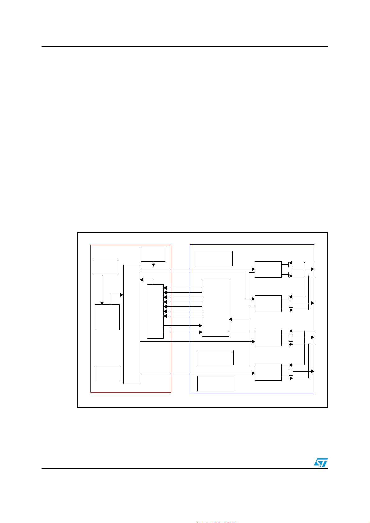
1.1 Block diagram
TM
family that provides full digital audio
2
S
Figure 1. Block diagram
I2C
I2S
interface
Power
Volume
control
PLL
FFX
control
Protection
current/thermal
Logic
Regulators
Bias
Channel
1A
Channel
1B
Channel
2A
Channel
2B
PowerDigital DSP
4/43
Page 5
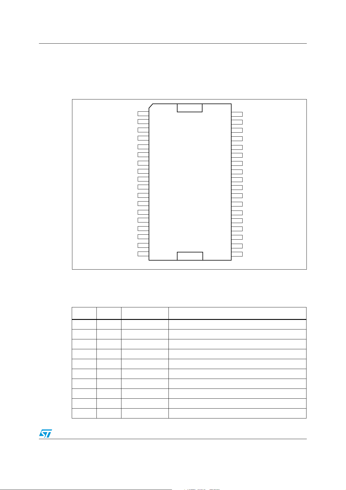
STA335W Pin connections
2 Pin connections
2.1 Connection diagram
Figure 2. Pin connection PowerSSO-36 (Top view)
GND_SUB
SA
TEST_MODE
VSS
VCC_REG
OUT2B
GND2
VCC2
OUT2A
OUT1B
VCC1
GND1
OUT1A
GND_REG
VDD
CONFIG
NC
NC
1
2
3
4
5
6
7
8
9
10
11
12
13
14
15
16
17
18
36
35
34
33
32
31
30
29
28
27
26
25
24
23
22
21
20
19
D05AU1638
VDD_DIG
GND_DIG
SCL
SDA
INT_LINE
RESET
SDI
LRCKI
BICKI
XTI
GND_PLL
FILTER_PLL
VDD_PLL
PWRDN
GND_DIG
VDD_DIG
NC
NC
2.2 Pin description
Table 2. Pin description
Pin Type Name Description
1 GND GND_SUB Substrate ground
2I SA I
3 I TEST_MODE This pin must be connected to ground (pull-down)
4 I/O VSS Internal reference at Vcc-3.3 V
5 I/O VCC_REG Internal Vcc reference
6 O OUT2B Output half bridge 2B
7 GND GND2 Power negative supply
8 Power VCC2 Power positive supply
9 O OUT2A Output half bridge 2A
10 O OUT1B Output half bridge 1B
2
C select address (pull-down)
5/43
Page 6

Pin connections STA335W
Table 2. Pin description (continued)
Pin Type Name Description
11 Power VCC1 Power positive supply
12 GND GND1 Power negative supply
13 O OUT1A Output half bridge 1A
14 GND GND_REG Internal ground reference
15 Power VDD Internal 3.3 V reference voltage
16 I CONFIG Paralleled mode command
17 O N.C. Not to be connected
18 O N.C. Not to be connected
19 O N.C. Not to be connected
20 I/O N.C. Not to be connected
21 Power VDD_DIG Digital supply voltage
22 GND GND_DIG Digital ground
23 I PWRDN Power down (pull-up)
24 Power VDD_PLL Positive supply for PLL
25 I FILTER_PLL Connection to PLL filter
26 GND GND_PLL Negative supply for PLL
27 I XTI PLL input clock
2
28 I BICKI I
29 I LRCKI I
30 I SDI I
S serial clock
2
S left/right clock
2
S serial data channels 1 and 2
31 I RESET Reset (pull-up)
32 O INT_LINE Fault interrupt
2
33 I/O SDA I
34 I SCL I
C serial data
2
C serial clock
35 GND GND_DIG Digital ground
36 Power VDD_DIG Digital supply voltage
6/43
Page 7
STA335W Electrical specifications
3 Electrical specifications
3.1 Absolute maximum ratings
Table 3. Absolute maximum ratings
Symbol Parameter Min Typ Max Unit
V
VDD_DIG Digital supply voltage -0.3 4 V
VDD_PLL PLL supply voltage -0.3 4
T
T
Power supply voltage (VCCxA, VCCxB) -0.3 30 V
cc
Operating junction temperature -20 150 °C
op
Storage temperature -40 150 °C
stg
Warning: Stresses beyond those listed in Table 3 may cause
permanent damage to the device. These are stress ratings
only, and functional operation of the device at these or any
other conditions beyond those indicated under
“Recommended operating conditions” are not implied.
Exposure to absolute-maximum-rated conditions for
extended periods may affect device reliability. In the real
application, power supplies with nominal values rated within
the recommended operating conditions, may experience
some rising beyond the maximum operating conditions for a
short time when no or very low current is sinked (amplifier in
mute state). In this case the reliability of the device is
guaranteed, provided that the absolute maximum ratings are
not exceeded.
3.2 Thermal data
Table 4. Thermal data
R
th j-case
T
th-sdj
T
th-w
T
th-sdh
R
th j-amb
1. See Section 7: Package thermal characteristics on page 39 for details.
Thermal resistance junction-case (thermal pad) 1.5 °C/W
Thermal shut-down junction temperature 150 °C
Thermal warning temperature 130 °C
Thermal shut-down hysteresis 20 °C
Thermal resistance junction-ambient
Parameter Min Typ Max Unit
(1)
7/43
Page 8

Electrical specifications STA335W
3.3 Recommended operating conditions
Table 5. Recommended operating condition
Symbol Parameter Min Typ Max Unit
V
Power supply voltage (VCCxA, VCCxB) 5 26 V
cc
VDD_DIG Digital supply voltage 2.7 3.3 3.6 V
VDD_PLL PLL supply voltage 2.7 3.3 3.6 V
Ambient temperature -20 70 °C
T
amb
3.4 Electrical specifications for the digital section
Table 6. Electrical specifications - digital section
Symbol Parameter Conditions Min Typ Max Unit
Low level input current without
I
il
pull-up/down device
I
V
V
V
V
I
R
High level input current without
ih
pull-up/down device
Low level input voltage
il
High level input voltage
ih
Low level output voltage Iol=2 mA
ol
High level output voltage Ioh=2 mA
oh
Pull-up/down current 25 66 125 µA
pu
Equivalent pull-up/down
pu
resistance
Vi = 0 V 1 10 µA
Vi = VDD_DIG
= 3.6 V
0.8 *
VDD_DIG
0.8 *
VDD_DIG
110µA
0.2 *
VDD_DIG
V
V
0.4 *
VDD_DIG
V
V
50 kΩ
8/43
Page 9

STA335W Electrical specifications
3.5 Electrical specifications for the power section
The specifications given in this section are valid for the operating conditions: VCC=18V,
f=1kHz, f
Table 7. Electrical specifications - power section
Symbol Parameter Conditions Min Typ Max Unit
= 384 kHz, T
sw
= 25° C and RL = 8 Ω, unless otherwise specified.
amb
Po Output power BTL
THD = 1% 16
THD = 10% 20
R
dsON
Power Pchannel/Nchannel MOSFET
(total bridge)
= 1.5 A 180 250 mΩ
l
d
gP Power Pchannel RdsON matching ld = 1.5 A 95 %
gN Power Nchannel RdsON matching l
= 1.5 A 95 %
d
Idss Power Pchannel/Nchannel leakage VCC = 20 V 10 μA
(1)
(1)
(1)
(1)
8 15 ns
15 30 ns
10 18 ns
10 18 ns
I
LDT
I
HDT
V
Low current dead time (static) Resistive load
High current dead time (dynamic) Iload = 1.5 A
Rise time Resistive load
t
r
Fall time Resistive load
t
f
Supply voltage operating voltage 5 26 V
cc
Supply current from Vcc in power down PWRDN = 0 0.1 1 mA
PCM Input signal = -
I
vcc
Supply current from Vcc in operation
60 dBfs,
Switching frequency
52 60 mA
= 384 kHz,
No LC filters
I
vdd
Supply current FFX processing (reference
only)
Ilim Overcurrent limit
Internal clock =
49.152 MHz
(2)
55 70 mA
3.0 3.8 A
W
Isc Short circuit protection Hi-Z output 4.0 4.2 A
UVL Under voltage protection 3.5 4.3 V
t
min
Output minimum pulse width No load 20 30 60 ns
DR Dynamic range 100 dB
Signal to noise ratio, ternary mode A-Weighted 100 dB
SNR
Signal to noise ratio binary mode 90 dB
FFX stereo mode,
<5 kHz
PSSR Power supply rejection ratio
V
RIPPLE
= 1 V RMS
80 dB
Audio input =
dither only
FFX stereo mode,
THD+N Total harmonic distortion + noise
Po = 1 W
0.2 %
f=1kHz
9/43
Page 10

Electrical specifications STA335W
Table 7. Electrical specifications - power section (continued)
Symbol Parameter Conditions Min Typ Max Unit
FFX stereo mode,
<5 kHz
X
TA L K
Crosstalk
Peak efficiency, FFX mode
η
Peak efficiency,binary modes
1. Refer to Figure 5: Test circuit 1.
2. Limit current if the register (OCRB par 6.1.3.3) overcurrent warning detect adjustment bypass is enabled. When disabled
refer to the Isc.
One channel driven
at 1 W
Other channel
measured
Po = 2 x 20 W
into 8 Ω
Po = 2 x 9 W into 4 Ω
+ 1 x 20 W into 8 Ω
80 dB
90
%
87
10/43
Page 11
STA335W Electrical specifications
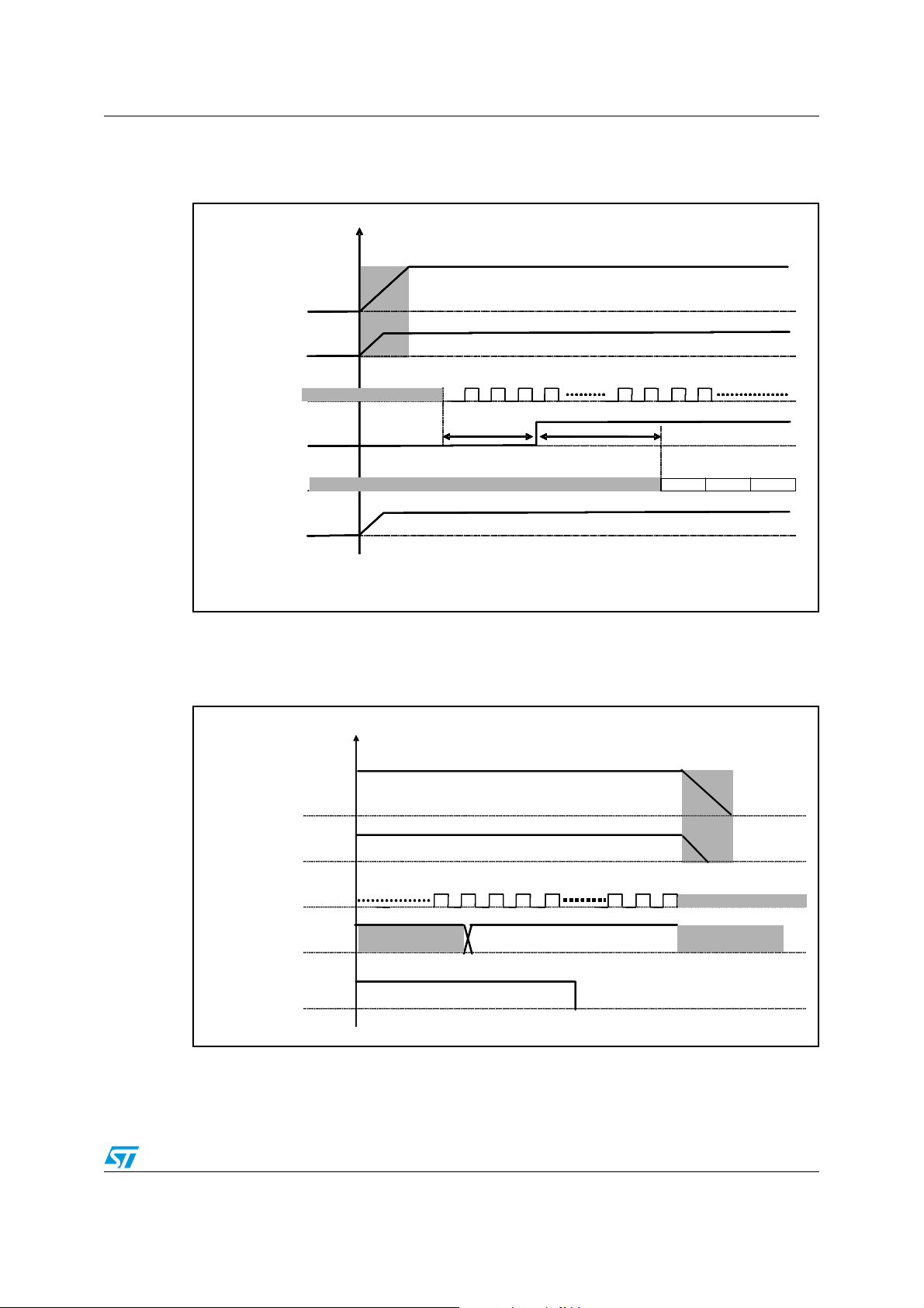
3.6 Power on/off sequence
Figure 3. Power-on sequence
VCC
VCC
VCC
VCC
VCC
VDD_Dig
VDD_Dig
VDD_Dig
VDD_Dig
VDD_Dig
XTI
XTI
XTI
XTI
XTI
Reset
Reset
Reset
Reset
Reset
2
2
2
2
2
C
C
C
C
C
I
I
I
I
I
PWDN
PWDN
PWDN
PWDN
PWDN
Note: no specific VCC and
VDD_DIG turn
is required
Don’t care
Don’t care
Don’t care
Don’t care
Don’t care
Don’t care
Don’t care
−
on sequence
TR
TR
TR
TR
TR
Don’t care
Don’t care
Don’t care
Don’t care
Don’t care
TC
TC
TC
TC
TC
CMD0 CMD1 CMD2
CMD0 CMD1 CMD2
CMD0 CMD1 CMD2
CMD0 CMD1 CMD2
CMD0 CMD1 CMD2
TR = minimum time between XTI master clock stable and Reset removal: 1 msec
TC = minimum time between Reset removal and I
Note: clock stable means: f
max
- f
< 1 MHz
min
2
C program, sequence start: 1msec
Note: see Chapter 5.2.3: Serial data first bit, for additional info.
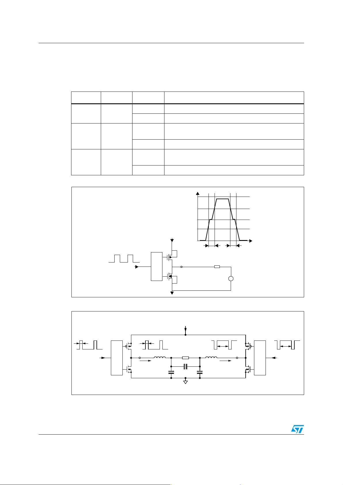
Figure 4. Power-off sequence for pop-free turn-off
VCC
VCC
VDD_Dig
VDD_Dig
XTI
XTI
Soft Mute
Soft Mute
Reg. 0x07
Reg. 0x07
Data 0xFE
Data 0xFE
Soft EAPD
Soft EAPD
Reg. 0x05
Reg. 0x05
Bit 7 = 0
Bit 7 = 0
Don’t care
Don’t care
FE
FE
Note: no specific VCC and
VDD_DIG turn
is required
Don’t care
Don’t care
Don’t care
Don’t care
−
off sequence
Don’t care
Don’t care
Don’t care
Don’t care
11/43
Page 12
Electrical specifications STA335W
3.7 Testing
3.7.1 Functional pin definition
Table 8. Functional pin definition
Pin name Number Logic value IC status
PWRDN 23
TWARN 20
EAPD 19
Figure 5. Test circuit 1
Low current dead time = MAX(DTr, DTf)
Duty cycle = 50%
INxY
0 Low consumption
1 Normal operation
0
A temperature warning is indicated by the external power
stage
1 Normal operation
0
Low consumption for power stage
All internal regulators are switched off
1 Normal operation
OUTxY
+Vcc
DTr DTf
M58
OUTxY
M57
gnd
R 8
Ω
V67
+
vdc = Vcc/2
Vcc
(3/4)Vcc
(1/2)Vcc
(1/4)Vcc
t
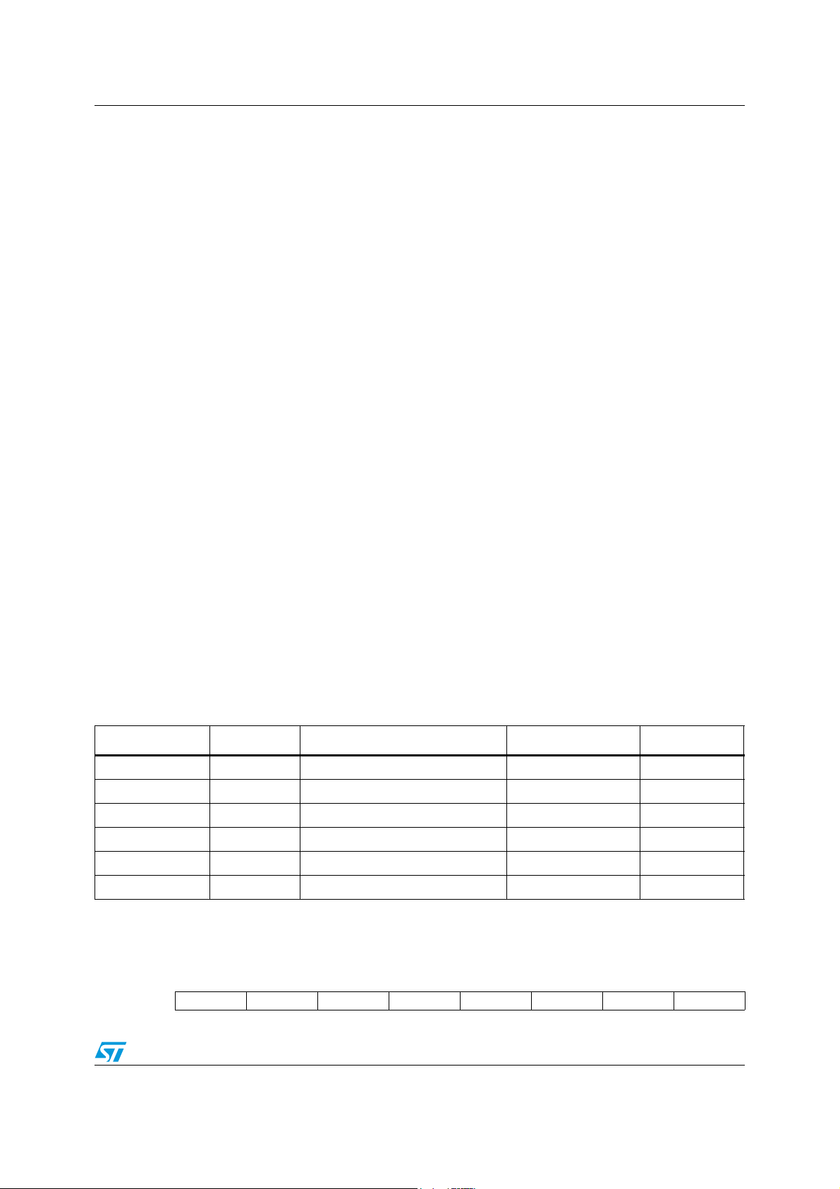
Figure 6. Test circuit 2
High Current Dead time for Bridge application = ABS(DTout(A)-DTin(A))+ABS(DTOUT(B)-DTin(B))
Duty cycle=A Duty cycle=B
M58
DTin(A)
INA
M57
Duty cycle A and B: Fixed to have DC output current of 4A in the direction shown in figure
12/43
Q1
Q3
OUTA
Iout=1.5A
DTout(A)
C69
470nF
+V
CC
Rload=4Ω
C71 470nF
M64
OUTB
Q2
M63
Q4
DTout(B) DTin(B)
L68 10μL67 10μ
Iout=1.5A
C70
470nF
INB
D06AU1651
Page 13

STA335W I2C bus specification
4 I2C bus specification
The STA335W supports the I2C protocol via the input ports SCL and SDA_IN (master to
slave) and the output port SDA_OUT (slave to master). This protocol defines any device
that sends data on to the bus as a transmitter and any device that reads the data as a
receiver. The device that controls the data transfer is known as the master and the other as
the slave. The master always starts the transfer and provides the serial clock for
synchronization. STA335W is always a slave device in all of its communications. It supports
up to 400 kb/s rate (fast-mode bit rate). STA335W I
4.1 Communication protocol
4.1.1 Data transition or change
Data changes on the SDA line must only occur when the SCL clock is low. SDA transition
while the clock is high is used to identify a START or STOP condition.
4.1.2 Start condition
START is identified by a high to low transition of the data bus SDA signal while the clock
signal SCL is stable in the high state. A START condition must precede any command for
data transfer.
2
C is a slave only interface.
4.1.3 Stop condition
STOP is identified by low to high transition of the data bus SDA signal while the clock signal
SCL is stable in the high state. A STOP condition terminates communication between
STA335W and the bus master.
4.1.4 Data input
During the data input the STA335W samples the SDA signal on the rising edge of clock
SCL. For correct device operation the SDA signal must be stable during the rising edge of
the clock and the data can change only when the SCL line is low.
4.2 Device addressing
To start communication between the master and the STA335W, the master must initiate with
a start condition. Following this, the master sends onto the SDA line 8-bits (MSB first)
corresponding to the device select address and read or write mode.
The seven most significant bits are the device address identifiers, corresponding to the I
bus definition. In the STA335W the I
the SA port configuration, 0x38 when SA = 0, and 0x3A when SA = 1.
The eighth bit (LSB) identifies read or write operation RW, this bit is set to 1 in read mode
and to 0 for write mode. After a START condition the STA335W identifies on the bus the
device address and if a match is found, it acknowledges the identification on SDA bus
during the 9th bit time. The byte following the device identification byte is the internal space
address.
2
C interface has two device addresses depending on
2
C
13/43
Page 14

I2C bus specification STA335W
4.3 Write operation
Following the START condition the master sends a device select code with the RW bit set
to 0. The STA335W acknowledges this and the writes for the byte of internal address. After
receiving the internal byte address the STA335W again responds with an
acknowledgement.
4.3.1 Byte write
In the byte write mode the master sends one data byte, this is acknowledged by the
STA335W. The master then terminates the transfer by generating a STOP condition.
4.3.2 Multi-byte write
The multi-byte write modes can start from any internal address. The master generating a
STOP condition terminates the transfer.
4.4 Read operation
4.4.1 Current address byte read
Following the START condition the master sends a device select code with the RW bit set
to 1. The STA335W acknowledges this and then responds by sending one byte of data. The
master then terminates the transfer by generating a STOP condition.
4.4.2 Current address multi-byte read
The multi-byte read modes can start from any internal address. Sequential data bytes are
read from sequential addresses within the STA335W. The master acknowledges each data
byte read and then generates a STOP condition terminating the transfer.
4.4.3 Random address byte read
Following the START condition the master sends a device select code with the RW bit set
to 0. The STA335W acknowledges this and then the master writes the internal address byte.
After receiving, the internal byte address the STA335W again responds with an
acknowledgement. The master then initiates another START condition and sends the device
select code with the RW bit set to 1. The STA335W acknowledges this and then responds
by sending one byte of data. The master then terminates the transfer by generating a STOP
condition.
4.4.4 Random address multi-byte read
The multi-byte read modes could start from any internal address. Sequential data bytes are
read from sequential addresses within the STA335W. The master acknowledges each data
byte read and then generates a STOP condition terminating the transfer.
14/43
Page 15

STA335W I2C bus specification
A
A
A
A
A
4.4.5 Write mode sequence
Figure 7. Write mode sequence
BYTE
WRITE
DEV-ADDR
START
MULTIBYTE
WRITE
DEV-ADDR
START
4.4.6 Read mode sequence
Figure 8. Read mode sequence
RW=
HIGH
ACK
RW
ACK
RW
ACK
ACK
RW
CURRENT
ADDRESS
READ
RANDOM
ADDRESS
READ
SEQUENTIAL
CURRENT
READ
SEQUENTIAL
RANDOM
READ
DEV-ADDR
START
DEV-ADDR
START
DEV-ADDR
START
DEV-ADDR
START
RW
RW
DATA
SUB-ADDR
DATA
SUB-ADDR
ACK
ACK
NO ACK
ACK
ACK
ACK
SUB-ADDR
SUB-ADDR
STOP
START RW
START RW
ACK
ACK
DEV-ADDR
DATA
DEV-ADDR
DATA IN
CK
STOP
DATA IN
CK
DATA IN
CK
STOP
ACK
ACK
ACK
DATA
DATA
DATA
NO ACK
NO ACK
CK
STOP
STOP
DATA
CK NO ACK
DATA
STOP
15/43
Page 16

Register description STA335W
5 Register description
Table 9. Register summary
Addr Name D7 D6 D5 D4 D3 D2 D1 D0
0x00 CONFA FDRB TWAB TWRB IR1 IR0 MCS2 MCS1 MCS0
0x01 CONFB C2IM C1IM Reserved SAIFB SAI3 SAI2 SAI1 SAI0
0x02 CONFC OCRB CSZ3 CSZ2 CSZ1 CSZ0 OM1 OM0
0x03 CONFD Reserved ZDE Reserved Reserved PSL Reserved Reserved Reserved
0x04 CONFE SVE ZCE DCCV PWMS AME NSBW MPC MPCV
0x05 CONFF EAPD PWDN ECLE LDTE BCLE IDE Reserved Reserved
0x06 MUTE/LOC Reserved Reserved Reserved Reserved Reserved C2M C1M MMUTE
0x07 MVOL MV7 MV6 MV5 MV4 MV3 MV2 MV1 MV0
0x08 C1VOL C1V7 C1V6 C1V5 C1V4 C1V3 C1V2 C1V1 C1V0
0x09 C2VOL C2V7 C2V6 C2V5 C2V4 C2V3 C2V2 C2V1 C2V0
0x0A Reserved
0x0B AUTO1 Reserved Reserved Reserved Reserved Reserved Reserved Reserved Reserved
0x0C AUTO2 Reserved Reserved Reserved Reserved AMAM2 AMAM1 AMAM0 AMAME
0x0D Reserved
0x0E C1CFG Reserved Reserved Reserved Reserved C1BO Reserved Reserved Reserved
0x0F C2CFG Reserved Reserved Reserved Reserved C2BO Reserved Reserved Reserved
0x10 Reserved
0x11 Reserved
0x12 Reserved
0x13 Reserved
0x14 Reserved
0x15 Reserved
0x16 CFADDR Reserved Reserved CFA5 CFA4 CFA3 CFA2 CFA1 CFA0
0x17 B1CF1 C1B23 C1B22 C1B21 C1B20 C1B19 C1B18 C1B17 C1B16
0x18 B1CF2 C1B15 C1B14 C1B13 C1B12 C1B11 C1B10 C1B9 C1B8
0x19 B1CF3 C1B7 C1B6 C1B5 C1B4 C1B3 C1B2 C1B1 C1B0
0x1A Reserved
0x1B Reserved
0x1C Reserved
0x1D Reserved
0x1E Reserved
0x1F Reserved
16/43
Page 17

STA335W Register description
Table 9. Register summary (continued)
Addr Name D7 D6 D5 D4 D3 D2 D1 D0
0x20 Reserved
0x21 Reserved
0x22 Reserved
0x23 Reserved
0x24 Reserved
0x25 Reserved
0x26 CFUD Reserved Reserved R1 Reserved W1
0x27 MPCC1 MPCC15 MPCC14 MPCC13 MPCC12 MPCC11 MPCC10 MPCC9 MPCC8
0x28 MPCC2 MPCC7 MPCC6 MPCC5 MPCC4 MPCC3 MPCC2 MPCC1 MPCC0
0x29 DCC1 DCC15 DCC14 DCC13 DCC12 DCC11 DCC10 DCC9 DCC8
0x2A DCC2 DCC7 DCC6 DCC5 DCC4 DCC3 DCC2 DCC1 DCC0
0x2B FDRC1 FDRC15 FDRC14 FDRC13 FDRC12 FDRC11 FDRC10 FDRC9 FDRC8
0x2C FDRC2 FDRC7 FDRC6 FDRC5 FDRC4 FDRC3 FDRC2 FDRC1 FDRC0
0x2D STATUS PLLUL FAULT UVFAULT OVFAULT OCFAULT OCWARN TFAULT TWARN
0x2E Reserved Reserved RO1BACT R5BACT R4BACT R3BACT R2BACT R1BACT
0x2F Reserved Reserved R01BEND R5BEND R4BEND R3BEND R2BEND R1BEND
0x30 Reserved Reserved R5BBAD R4BBAD R3BBAD R2BBAD R1BBAD
0x31 EQCFG XOB Reserved Reserved AMGC3 AMGC2 Reserved SEL1 SEL0
0x32 Reserved
0x33 Reserved
0x34 Reserved
0x35 Reserved
0x36 Reserved
0x37 Reserved Reserved SVUPE SVUP[4] SVUP[3] SVUP[2] SVUP[1] SVUP[0]
0x38 Reserved Reserved SVDWE SVDW[4] SVDW[3] SVDW[2] SVDW[1] SVDW[0]
5.1 Configuration register A (addr 0x00)
D7 D6 D5 D4 D3 D2 D1 D0
FDRB TWAB TWRB IR1 IR0 MCS2 MCS1 MCS0
01100011
17/43
Page 18

Register description STA335W
5.1.1 Master clock select
Table 10. Master clock select
Bit R/W RST Name Description
0R/W 1 MCS0
1R/W 1 MCS1
Selects the ratio between the input I
frequency and the input clock.
2
S sample
2R/W 0 MCS2
The STA335W supports sample rates of 32 kHz, 44.1 kHz, 48 kHz, 88.2 kHz, 96 kHz,
176.4 kHz, and 192 kHz. Therefore the internal clock is:
● 32.768 MHz for 32 kHz
● 45.1584 MHz for 44.1 kHz, 88.2 kHz, and 176.4 kHz
● 49.152 MHz for 48 kHz, 96 kHz, and 192 kHz
The external clock frequency provided to the XTI pin must be a multiple of the input sample
frequency (f
).
s
The relationship between the input clock and the input sample rate is determined by both
the MCSx and the IR (input rate) register bits. The MCSx bits determine the PLL factor
generating the internal clock and the IR bit determines the oversampling ratio used
internally.
Table 11. Input sampling rates
Input sample rate
fs (kHz)
IR MCS[2:0]
101 100 011 010 001 000
32, 44.1, 48 00 576 * fs 128 * fs 256 * fs 384 * fs 512 * fs 768 * fs
88.2, 96 01 NA 64 * fs 128 * fs 192 * fs 256 * fs 384 * fs
176.4, 192 1X NA 32 * fs 64 * fs 96 * fs 128 * fs 192 * fs
18/43
Page 19

STA335W Register description
5.1.2 Interpolation ratio select
Table 12. Internal interpolation ratio
Bit R/W RST Name Description
4:3 R/W 00 IR [1:0]
Selects internal interpolation ratio based on input I
sample frequency
The STA335W has variable interpolation (oversampling) settings such that internal
processing and FFX output rates remain consistent. The first processing block interpolates
by either 2-times or 1-time (pass-through) or provides a 2-times downsample. The
oversampling ratio of this interpolation is determined by the IR bits.
Table 13. IR bit settings as a function of input sample rate
Input sample rate fs (kHz) IR 1st stage interpolation ratio
32 00 2 times oversampling
44.1 00 2 times oversampling
48 00 2 times oversampling
88.2 01 Pass-through
96 01 Pass-through
176.4 10 2 times downsampling
192 10 2 times downsampling
2
S
5.1.3 Thermal warning recovery bypass
Table 14. Thermal warning recovery bypass
Bit R/W RST Name Description
5R/W 1 TWRB
0: Thermal warning recovery enabled
1: Thermal warning recovery disabled
If the thermal warning adjustment is enabled (TWAB = 0), then the thermal warning recovery
determines if the -3 dB output limit is removed when thermal warning is negative.
If TWRB = 0 and TWAB = 0, then when a thermal warning disappears the -3 dB output limit
is removed and the gain is added back to the system. If TWRB = 1 and TWAB = 0, then
when a thermal warning disappears the -3 dB output limit remains until TWRB is changed to
zero or the device is reset.
5.1.4 Thermal warning adjustment bypass
Table 15. Thermal warning adjustment bypass
Bit R/W RST Name Description
6R/W 1 TWAB
The on-chip STA335W power output block provides feedback to the digital controller using
inputs to the power control block. Input TWARN is used to indicate a thermal warning
0: Thermal warning adjustment enabled
1: Thermal warning adjustment disabled
19/43
Page 20

Register description STA335W
condition. When TWARN is asserted (set to 0) for a period of time greater than 400 ms, the
power control block forces a -3 dB output limit (determined by TWOCL in the coefficient
RAM) to the modulation limit in an attempt to eliminate the thermal warning condition. Once
the thermal warning output limit adjustment is applied, it remains in this state until reset,
unless FDRB = 0.
5.1.5 Fault detect recovery bypass
Table 16. Fault detect recovery bypass
Bit R/W RST Name Description
7R/W 0 FDRB
0: fault detect recovery enabled
1: fault detect recovery disabled
The on-chip STA335W power output block provides feedback to the digital controller using
inputs to the power control block. The FAULT input is used to indicate a fault condition
(either over-current or thermal). When FAULT is asserted (set to 0), the power control block
attempts a recovery from the fault by asserting the tri-state output (setting it to 0 which
directs the power output block to begin recovery), holds it at 0 for period of time in the range
of 0.1 ms to 1 second as defined by the fault-detect recovery constant register (FDRC
registers 0x29-0x2A), then toggles it back to 1. This sequence is repeated as log as the fault
indication exists. This feature is enabled by default but can be bypassed by setting the
FDRB control bit to 1.
5.2 Configuration register B (addr 0x01)
D7 D6 D5 D4 D3 D2 D1 D0
C2IM C1IM DSCKE SAIFB SAI3 SAI2 SAI1 SAI0
10000000
5.2.1 Serial audio input interface format
Table 17. Serial audio input interface
Bit R/W RST Name Description
0 R/W 0 SAI0
1 R/W 0 SAI1
2 R/W 0 SAI2
3 R/W 0 SAI3
20/43
Determines the interface format of the input serial
digital audio interface.
Page 21

STA335W Register description
5.2.2 Serial data interface
The STA335W audio serial input was designed to interface with standard digital audio
components and to accept a number of serial data formats. STA335W always acts as slave
when receiving audio input from standard digital audio components. Serial data for two
channels is provided using three inputs: left/right clock LRCKI, serial clock BICKI, and serial
data 1 and 2 SDI12.
The SAI bits (D3 to D0) and the SAIFB bit (D4) are used to specify the serial data format.
The default serial data format is I
and figure that follow.
5.2.3 Serial data first bit
Table 18. Serial data first bit
SAIFB Format
0 MSB-first
1 LSB-first
Table 19. Support serial audio input formats for MSB-first (SAIFB = 0)
BICKI SAI [3:0] SAIFB Interface format
32 * fs
48 * fs
2
S, MSB-first. Available formats are shown in the tables
0000 0 I
0001 0 Left/right-justified 16-bit data
0000 0 I2S 16 to 23-bit data
0001 0 Left-justified 16 to 24-bit data
0010 0 Right-justified 24-bit data
0110 0 Right-justified 20-bit data
1010 0 Right-justified 18-bit data
1110 0 Right-justified 16-bit data
2
S 15-bit data
64 * fs
0000 0 I2S 16 to 24-bit data
0001 0 Left-justified 16 to 24-bit data
0010 0 Right-justified 24-bit data
0110 0 Right-justified 20-bit data
1010 0 Right-justified 18-bit data
1110 0 Right-justified 16-bit data
21/43
Page 22

Register description STA335W
Table 20. Supported serial audio input formats for LSB-first (SAIFB = 1)
BICKI SAI [3:0] SAIFB Interface Format
32 * fs
1100 1 I
1110 1 Left/right-justified 16-bit data
0100 1 I
0100 1 I
1000 1 I
1100 1 LSB first I
0001 1 Left-justified 24-bit data
0101 1 Left-justified 20-bit data
48 * fs
1001 1 Left-justified 18-bit data
1101 1 Left-justified 16-bit data
0010 1 Right-justified 24-bit data
0110 1 Right-justified 20-bit data
1010 1 Right-justified 18-bit data
1110 1 Right-justified 16-bit data
2
S 15-bit data
2
S 23-bit data
2
S 20-bit data
2
S 18-bit data
2
S 16-bit data
0000 1 I2S 24-bit data
2
0100 1 I
1000 1 I
1100 1 LSB first I
S 20-bit data
2
S 18-bit data
2
S 16-bit data
0001 1 Left-justified 24-bit data
0101 1 Left-justified 20-bit data
64 * fs
1001 1 Left-justified 18-bit data
1101 1 Left-justified 16-bit data
0010 1 Right-justified 24-bit data
0110 1 Right-justified 20-bit data
1010 1 Right-justified 18-bit data
1110 1 Right-justified 16-bit data
To make the STA335W work properly, the serial audio interface LRCKI clock must be
synchronous to the PLL output clock. It means that:
■ the frequency of PLL clock / frequency of LRCKI = N ±4 cycles,
where N depends on the settings in Table 13 on page 19
■ the PLL must be locked.
If these two conditions are not met, and IDE bit (reg 0x05 bit 2) is set to 1, the STA335W will
immediately mute the I
2
S PCM data out (provided to the processing block) and it will freeze
any active processing task.
To avoid any audio side effects (like pop noise), it is strongly recommended to soft mute any
audio streams flowing into STA335W data path before the desynchronization event
22/43
Page 23

STA335W Register description
happens. At the same time any processing related to the I2C configuration should be issued
only after the serial audio interface and the internal PLL are synchronous again.
Note: Any mute or volume change causes some delay in the completion of the I
2
C operation due
to the soft volume feature. The soft volume phase change must be finished before any clock
desynchronization.
5.2.4 Channel input mapping
Table 21. Channel input mapping
Bit R/W RST Name Description
2
6R/W 0 C1IM
7R/W 1 C2IM
0: Processing channel 1 receives Left I
1: Processing channel 1 receives Right I2S Input
0: Processing channel 2 receives Left I
1: Processing channel 2 receives Right I2S Input
Each channel received via I2S can be mapped to any internal processing channel via the
Channel Input Mapping registers. This allows for flexibility in processing. The default
settings of these registers map each I
2
S input channel to its corresponding processing
channel.
S Input
2
S Input
23/43
Page 24

Register description STA335W
5.3 Configuration register C (addr 0x02)
D7 D6 D5 D4 D3 D2 D1 D0
OCRB CSZ3 CSZ2 CSZ1 CSZ0 OM1 OM0
1 011111
5.3.1 FFX power output mode
Table 22. FFX power output mode
Bit R/W RST Name Description
0R/W 1 OM0
Selects configuration of FFX output.
1R/W 1 OM1
The FFX power output mode selects how the FFX output timing is configured.
Different power devices use different output modes.
Table 23. Output modes
OM[1,0] Output stage mode
00 Drop compensation
01 Discrete output stage - tapered compensation
10 Full power mode
11 Variable drop compensation (CSZx bits)
5.3.2 FFX compensating pulse size register
Table 24. FFX compensating pulse size bits
Bit R/W RST Name Description
2R/W 1 CSZ0
3R/W 1 CSZ1
4R/W 1 CSZ2
5R/W 0 CSZ3
Table 6:
Table 25. Compensating pulse size
When OM[1,0] = 11, this register determines the size
of the FFX compensating pulse from 0 clock ticks to
15 clock periods.
CSZ[3:0] Compensating Pulse Size
0000 0 ns (0 tick) compensating pulse size
0001 20 ns (1 tick) clock period compensating pulse size
……
1111 300 ns (15 tick) clock period compensating pulse size
24/43
Page 25

STA335W Register description
5.3.3 Over-current warning detect adjustment bypass
Table 26. Over-current warning bypass
Bit R/W RST Name Description
7 R/W 1 OCRB
0: Over-Current warning adjustment enabled
1: Over-Current warning adjustment disabled
The OCWARN input is used to indicate an over-current warning condition. When OCWARN
is asserted (set to 0), the power control block forces an adjustment to the modulation limit
(default is -3 dB) in an attempt to eliminate the over-current warning condition. Once the
over-current warning volume adjustment is applied, it remains in this state until reset is
applied. The level of adjustment can be changed via the TWOCL (thermal warning/over
current limit) setting which is address 0x37 of the user defined coefficient RAM.
5.4 Configuration register D (addr 0x03)
D7 D6 D5 D4 D3 D2 D1 D0
Reserved ZDE Reserved Reserved PSL Reserved Reserved Reserved
01000000
5.4.1 Post-scale link
Table 27. Post-scale link
Bit R/W RST Name Description
3 R/W 0 PSL
0: Each channel uses individual post-scale value
1: Each channel uses channel 1 post-scale value
Post-scale functionality can be used for power-supply error correction. For multi-channel
applications running off the same power-supply, the post-scale values can be linked to the
value of channel 1 for ease of use and update the values faster.
5.4.2 Zero-detect mute enable
Table 28. Zero-detect mute enable
Bit R/W RST Name Description
6 R/W 1 ZDE Setting of 1 enables the automatic zero-detect mute
Setting the ZDE bit enables the zero-detect automatic mute. The zero-detect circuit looks at
the data for each processing channel at the output of the crossover (bass management)
filter. If any channel receives 2048 consecutive zero value samples (regardless of fs) then
that individual channel is muted if this function is enabled.
5.5 Configuration register E (addr 0x04)
D7 D6 D5 D4 D3 D2 D1 D0
SVE ZCE DCCV PWMS AME NSBW MPC MPCV
25/43
Page 26

Register description STA335W
D7 D6 D5 D4 D3 D2 D1 D0
11000010
5.5.1 Max power correction variable
Table 29. Max power correction variable
Bit R/W RST Name Description
0R/W 0 MPCV
5.5.2 Max power correction
Table 30. Max power correction
Bit R/W RST Name Description
1R/W 1 MPC
Setting the MPC bit turns on special processing that corrects the STA335W power device at
high power. This mode should lower the THD+N of a full FFX system at maximum power
output and slightly below. If enabled, MPC is operational in all output modes except tapered
(OM[1,0] = 01) and binary. When OCFG = 00, MPC will not effect channels 3 and 4, the lineout channels.
5.5.3 Noise-shaper bandwidth selection
Table 31. Noise-shaper bandwidth selection
Bit R/W RST Name Description
2 R/W 0 NSBW
1: Third order NS
0: Fourth order NS
0: Use standard MPC coefficient
1: Use MPCC bits for MPC coefficient
Setting of 1 enables Power Bridge correction for
THD reduction near maximum power output.
5.5.4 AM mode enable
Table 32. AM mode enable
Bit R/W RST Name Description
3R/W 0 AME
STA335W features aFFX processing mode that minimizes the amount of noise generated in
frequency range of AM radio. This mode is intended for use when FFX is operating in a
device with an AM tuner active. The SNR of the FFX processing is reduced to approximately
83 dB in this mode, which is still greater than the SNR of AM radio.
26/43
0: Normal FFX operation.
1: AM reduction mode FFX operation
Page 27

STA335W Register description
5.5.5 PWM speed mode
Table 33. PWM speed mode
Bit R/W RST Name Description
4R/W 0 PWMS
0: Normal speed (384 kHz) all channels
1: Odd speed (341.3 kHz) all channels
5.5.6 Distortion compensation variable enable
Table 34. Distortion compensation variable enable
Bit R/W RST Name Description
5R/W 0 DCCV
0: Use preset DC coefficient
1: Use DCC coefficient
5.5.7 Zero-crossing volume enable
Table 35. Zero-crossing volume enable
Bit R/W RST Name Description
1: Volume adjustments only occur at digital zero-
6R/W 1 ZCE
The ZCE bit enables zero-crossing volume adjustments. When volume is adjusted on digital
zero-crossings no clicks are audible.
crossings
0: Volume adjustments occur immediately
5.5.8 Soft volume update enable
Table 36. Soft volume update enable
Bit R/W RST Name Description
7R/W 1 SVE
1: Volume adjustments ramp according to SVR settings
0: Volume adjustments occur immediately
5.6 Configuration register F (addr 0x05)
D7 D6 D5 D4 D3 D2 D1 D0
EAPD PWDN ECLE LDTE BCLE IDE Reserved Reserved
01011100
27/43
Page 28

Register description STA335W
5.6.1 Invalid input detect mute enable
Table 37. Invalid input detect mute enable
Bit R/W RST Name Description
2R/W 1 IDE
Setting of 1 enables the automatic invalid input
detect mute
Setting the IDE bit enables this function, which looks at the input I2S data and automatically
mutes if the signals are perceived as invalid.
5.6.2 Binary output mode clock loss detection
Table 38. Binary output mode clock loss detection
Bit R/W RST Name Description
3 R/W 1 BCLE Binary output mode clock loss detection enable
Detects loss of input MCLK in binary mode and will output 50% duty cycle.
5.6.3 LRCK double trigger protection
Table 39. LRCK double trigger protection
Bit R/W RST Name Description
4 R/W 1 LDTE LRCLK double trigger protection enable
Actively prevents double trigger of LRCLK.
5.6.4 Auto EAPD on clock loss
Table 40. Auto EAPD on clock loss
Bit R/W RST Name Description
5 R/W 0 ECLE Auto EAPD on clock loss
When active, issues a power device power down signal (EAPD) on clock loss detection.
5.6.5 IC power down
Table 41. IC power down
Bit R/W RST Name Description
6R/W 1 PWDN
The PWDN register is used to place the IC in a low-power state. When PWDN is written
as 0, the output begins a soft-mute. After the mute condition is reached, EAPD is asserted
to power down the power-stage, then the master clock to all internal hardware expect the
2
I
C block is gated. This places the IC in a very low power consumption state.
28/43
0: IC power down low-power condition
1: IC normal operation
Page 29
STA335W Register description
5.6.6 Amplifier power down
Table 42. External amplifier power down
Bit R/W RST Name Description
7 R/W 0 EAPD
0: Power stage power down active
1: Normal operation
The EAPD register directly disables/enables the internal power circuitry.
When EAPD = 0, the internal power section is placed on a low-power state (disabled).
5.7 Volume control registers (addr 0x06 - 0x0A)
5.7.1 Mute/line output configuration register
D7 D6 D5 D4 D3 D2 D1 D0
LOC1 LOC0 Reserved Reserved C3M C2M C1M MMUTE
00000000
Table 43. Line output configuration
LOC[1:0] Line output configuration
00 Line output fixed - no volume, no EQ
01 Line output variable - CH3 volume effects line output, no EQ
10 Line output variable with EQ - CH3 volume effects line output
Line output is only active when OCFG = 00. In this case LOC determines the line output
configuration. The source of the line output is always the channel 1 and 2 inputs.
5.7.2 Master volume register
D7 D6 D5 D4 D3 D2 D1 D0
MV7 MV6 MV5 MV4 MV3 MV2 MV1 MV0
11111111
5.7.3 Channel 1 volume
D7 D6 D5 D4 D3 D2 D1 D0
C1V7 C1V6 C1V5 C1V4 C1V3 C1V2 C1V1 C1V0
01100000
5.7.4 Channel 2 volume
D7 D6 D5 D4 D3 D2 D1 D0
C2V7 C2V6 C2V5 C2V4 C2V3 C2V2 C2V1 C2V0
01100000
29/43
Page 30

Register description STA335W
The Volume structure of the STA335W consists of individual volume registers for each
channel and a master volume register that provides an offset to each channels volume
setting. The individual channel volumes are adjustable in 0.5 dB steps from +48 dB to 80 dB.
As an example if C1V = 0x00 or +48 dB and MV = 0x18 or -12 dB, then the total gain for
channel 1 = +36 dB.
The master mute, when set to 1, mutes all channels at once, whereas the individual channel
mutes (CxM) mutes only that channel. Both the master mute and the channel mutes provide
a “soft mute” with the volume ramping down to mute in 4096 samples from the maximum
volume setting at the internal processing rate (approximately 96 kHz).
A “hard (instantaneous) mute” can be obtained by programming a value of 0xFF (255) to
any channel volume register or the master volume register. When volume offsets are
provided via the master volume register any channel whose total volume is less than -80 dB
is muted.
All changes in volume take place at zero-crossings when ZCE = 1 (Configuration register E
(addr 0x04) on page 25) on a per channel basis as this creates the smoothest possible
volume transitions. When ZCE = 0, volume updates occur immediately.
Table 44. Master volume offset as a function of MV[7:0]
MV[7:0] Volume offset from channel value
00000000 (0x00) 0 dB
00000001 (0x01) -0.5 dB
00000010 (0x02) -1 dB
……
01001100 (0x4C) -38 dB
……
11111110 (0xFE) -127.5 dB
11111111 (0xFF) Hard master mute
Table 45. Channel volume as a function of CxV[7:0]
CxV[7:0] Volume
00000000 (0x00) +48 dB
00000001 (0x01) +47.5 dB
00000010 (0x02) +47 dB
……
01011111 (0x5F) +0.5 dB
01100000 (0x60) 0 dB
01100001 (0x61) -0.5 dB
……
11010111 (0xD7) -59.5 dB
11011000 (0xD8) -60 dB
30/43
Page 31

STA335W Register description
Table 45. Channel volume as a function of CxV[7:0] (continued)
CxV[7:0] Volume
11011001 (0xD9) -61 dB
11011010 (0xDA) -62 dB
……
11101100 (0xEC) -80 dB
11101101 (0xED) Hard channel mute
……
11111111 (0xFF) Hard channel mute
5.8 Audio preset registers (0x0C)
5.8.1 Audio preset register 2 (addr 0x0C)
D7 D6 D5 D4 D3 D2 D1 D0
XO3 XO2 XO1 XO0 AMAM2 AMAM1 AMAM0 AMAME
00000000
5.8.2 AM interference frequency switching
Table 46. AM interference frequency switching bits
Bit R/W RST Name Description
Audio preset AM enable
0 R/W 0 AMAME
Table 47. Audio preset AM switching frequency selection
AMAM[2:0] 48 kHz/96 kHz input fs 44.1 kHz/88.2 kHz input fs
000 0.535 MHz - 0.720 MHz 0.535 MHz - 0.670 MHz
001 0.721 MHz - 0.900 MHz 0.671 MHz - 0.800 MHz
010 0.901 MHz - 1.100 MHz 0.801 MHz - 1.000 MHz
011 1.101 MHz - 1.300 MHz 1.001 MHz - 1.180 MHz
100 1.301 MHz - 1.480 MHz 1.181 MHz - 1.340 MHz
101 1.481 MHz - 1.600 MHz 1.341 MHz - 1.500 MHz
110 1.601 MHz - 1.700 MHz 1.501 MHz - 1.700 MHz
0: switching frequency determined by PWMS setting
1: switching frequency determined by AMAM settings
31/43
Page 32

Register description STA335W
5.9 User-defined coefficient control registers (addr 0x16 - 0x26)
5.9.1 Coefficient address register
D7 D6 D5 D4 D3 D2 D1 D0
CFA5 CFA4 CFA3 CFA2 CFA1 CFA0
000000
5.9.2 Coefficient data register bits 23:16
D7 D6 D5 D4 D3 D2 D1 D0
C1B23 C1B22 C1B21 C1B20 C1B19 C1B18 C1B17 C1B16
00000000
5.9.3 Coefficient data register bits 15:8
D7 D6 D5 D4 D3 D2 D1 D0
C1B15 C1B14 C1B13 C1B12 C1B11 C1B10 C1B9 C1B8
00000000
5.9.4 Coefficient data register bits 7:0
D7 D6 D5 D4 D3 D2 D1 D0
C1B7 C1B6 C1B5 C1B4 C1B3 C1B2 C1B1 C1B0
00000000
5.9.5 Coefficient write/read control register
D7 D6 D5 D4 D3 D2 D1 D0
Reserved Reserved R1 Reserved W1
0 0000
Coefficients for user-defined scaling are handled internally in the STA335W via RAM.
Access to this RAM is available to the user via an I
registers are dedicated to this function. One contains a coefficient base address, five sets of
three store the values of the 24-bit coefficients to be written or that were read, and one
contains bits used to control the write/read of the coefficient(s) to/from RAM.
Note: The read and write operation on RAM coefficients works only if LRCKI (pin 29) is switching.
Reading a coefficient from RAM
1. Select the RAM block with register 0x31 bit1, bit0.
2. Write 6-bits of address to I
3. Write 1 to R1 bit in I
4. Read top 8-bits of coefficient in I
5. Read middle 8-bits of coefficient in I
6. Read bottom 8-bits of coefficient in I
2
C register 0x16.
2
C address 0x26.
2
C address 0x17.
2
C address 0x18.
2
C address 0x19.
2
C register interface. A collection of I2C
32/43
Page 33
STA335W Register description
Writing a single coefficient to RAM
1. Select the RAM block with register 0x31 bit1, bit0.
2. Write 6-bits of address to I
3. Write top 8-bits of coefficient in I
4. Write middle 8-bits of coefficient in I
5. Write bottom 8-bits of coefficient in I
6. Write 1 to W1 bit in I
2
C register 0x16.
2
C address 0x17.
2
C address 0x26.
2
C address 0x18.
2
C address 0x19.
5.9.6 Post-scale
The STA335W provides one additional multiplication after the last interpolation stage and
the distortion compensation on each channel. This post-scaling is accomplished by using a
24-bit signed fractional multiplier, with 0x800000 = -1 and 0x7FFFFF = 0.9999998808. The
scale factor for this multiply is loaded into RAM using the same I
coefficients and the bass-management. This post-scale factor can be used in conjunction
with an ADC equipped micro-controller to perform power-supply error correction. All
channels can use the channel-1 post-scale factor by setting the post-scale link bit. By
default, all post-scale factors are set to 0x7FFFFF. When line output is being used,
channel-3 post-scale will affect both channels 3 and 4.
2
C registers as the biquad
5.9.7 Over-current post-scale
The STA335W provides a simple mechanism for reacting to over-current detection in the
power-block. When the ocwarn input is asserted, the over-current post-scale value is used
in place of the normal post-scale value to provide output attenuation on all channels. The
default setting provides 3 dB of output attenuation when ocwarn is asserted.
The amount of attenuation to be applied in this situation can be adjusted by modifying the
Over-current Post-scale value. As with the normal post-scale, this scaling value is a 24-bit
signed fractional multiplier, with 0x800000 = -1 and 0x7FFFFF = 0.9999998808. By default,
the over-current post-scale factor is set to
applied, it remains until the device is reset.
Table 48. RAM block for scaling management
Index (Decimal) Index (Hex) Coefficient Default
0 Reserved
…… Reserved
52 0x34 Channel 1 - Post-Scale C1PstS 0x7FFFFF
53 0x35 Channel 2 - Post-Scale C2PstS 0x7FFFFF
54 0x36 Reserved
55 0x37 TWARN/OC - Limit TWOCL 0x5A9DF7
0x5A9DF7. Once the over-current attenuation is
5.10 Variable max power correction registers (addr 0x27 - 0x28)
D7 D6 D5 D4 D3 D2 D1 D0
MPCC15 MPCC14 MPCC13 MPCC12 MPCC11 MPCC10 MPCC9 MPCC8
33/43
Page 34

Register description STA335W
D7 D6 D5 D4 D3 D2 D1 D0
00011010
D7 D6 D5 D4 D3 D2 D1 D0
MPCC7 MPCC6 MPCC5 MPCC4 MPCC3 MPCC2 MPCC1 MPCC0
11000000
MPCC bits determine the 16 MSBs of the MPC compensation coefficient. This coefficient is
used in place of the default coefficient when MPCV = 1.
5.11 Variable distortion compensation registers (addr 0x29 0x2A)
D7 D6 D5 D4 D3 D2 D1 D0
DCC15 DCC14 DCC13 DCC12 DCC11 DCC10 DCC9 DCC8
11110011
D7 D6 D5 D4 D3 D2 D1 D0
DCC7 DCC6 DCC5 DCC4 DCC3 DCC2 DCC1 DCC0
00110011
DCC bits determine the 16 MSBs of the Distortion compensation coefficient. This coefficient
is used in place of the default coefficient when DCCV = 1.
5.12 Fault detect recovery constant registers (addr 0x2B - 0x2C)
D7 D6 D5 D4 D3 D2 D1 D0
FDRC15 FDRC14 FDRC13 FDRC12 FDRC11 FDRC10 FDRC9 FDRC8
00000000
D7 D6 D5 D4 D3 D2 D1 D0
FDRC7 FDRC6 FDRC5 FDRC4 FDRC3 FDRC2 FDRC1 FDRC0
00001100
FDRC bits specify the 16-bit fault detect recovery time delay. When FAULT is asserted, the
TRISTATE output is immediately asserted low and held low for the time period specified by
this constant. A constant value of 0x0001 in this register is approximately 0.083 ms. The
default value of 0x000C gives approximately 0.1 ms.
5.13 Device status register (addr 0x2D)
D7 D6 D5 D4 D3 D2 D1 D0
PLLUL FAULT UVFAULT OVFAULT OCFAULT OCWARN TFAULT TWARN
This read-only register provides fault and thermal-warning status information from the power
control block. Logic value 1 for faults or warning means normal state. Logic 0 means a fault
or warning detected on power bridge. The PLLUL = 1 means that the PLL is not locked.
34/43
Page 35

STA335W Register description
Table 49. Status register bits
Bit R/W RST Name Description
0:
7 R - PLLUL
6R - FAULT
5R - UVFAULT
PLL locked
1: PLL not locked
0: fault detected on power bridge
1: normal operation
0: VCCxX internally detected
< undervoltage threshold
4R - OVFAULT
0: VCCxX internally detected
> overvoltage threshold
3 R - OCFAULT 0: overcurrent fault detected
2 R - OCWARN 0: overcurrent warning
1R - TFAULT
0R - TWARN
0: thermal fault, junction temperature over limit
detection
0: thermal warning, junction temperature is close to
the fault condition
5.13.1 Extended Soft Volume configuration registers (addr 0x37 - 0x38)
D7 D6 D5 D4 D3 D2 D1 D0
SVUPE SVUP[4] SVUP[3] SVUP[2] SVUP[1] SVUP[0]
00000000
D7 D6 D5 D4 D3 D2 D1 D0
SVDWE SVDW4] SVDW[3] SVDW[2] SVDW[1] SVDW[0]
00000000
Soft volume update has a fixed rate by default. Using register 0x37 and 0x38 it is possible to
override the default behavior allowing different volume change rates.
It is also possible to independently define the fade-in (volume is increased) and fade-out
(volume is decreased) rates according to the desired behavior.
SVUPE Mode
0 When volume is increased, use the default rate
1 When volume is increased, use the rates defined by SVUP[4:0] .
When SVUPE = 1 the fade-in rate is defined by the SVUP[4:0] bits according to the
following formula:
Fade-in rate = 48 / (N + 1) dB/ms
where N is the SVUP[4:0] value.
SVDWE Mode
0 When volume is decreased, use the default rate
1 When volume is decreased, use the rates defined by SVDW[4:0] .
35/43
Page 36

Register description STA335W
When SVDWE = 1 the fade-out rate is defined by the SVDW[4:0] bits according to the
following formula:
Fade-in rate = 48 / (N + 1) dB/ms
where N is the SVDW[4:0] value.
36/43
Page 37

STA335W Application
6 Application
6.1 Application scheme for power supplies
Here in the next figure the typical application scheme for STA335W concerning the power
supplies. A particular care has to be devoted to the layout of the PCB. In particular all the
decoulpling capacitors have to be put as much as possible closed to the device to limit
spikes on all the supplies.
Figure 9. Application scheme for power supplies
6.2 PLL filter schematic
It is recommended to use the above scheme and values for the PLL loop filter to achieve the
best performances from the device in general application. Please be noted that the ground
of this filter scheme has to be connected to the ground of the PLL without any resistive path.
Concerning the component values, please take into account that the greater is the filter
bandwidth, the less is the lock time but the higher is the PLL output jitter.
6.3 Typical output configuration
Here after the typical output configuration used for BTL stereo mode. Please refer to the
application note for all the other possible output configuration recommended schematics.
37/43
Page 38
Application STA335W
Figure 10. Output configuration for stereo BTL mode
22uH
22uH
22
22
22
330pF
330pF
330pF
22
22
22
330pF
330pF
330pF
22uH
22uH
22uH
22uH
22uH
22uH
22uH
6.2
6.2
6.2
6.2
6.2
6.2
6.2
6.2
6.2
6.2
6.2
6.2
100nF
100nF
100nF
100nF
100nF
100nF
100nF
100nF
100nF
100nF
100nF
100nF
100nF
100nF
100nF
100nF
100nF
100nF
100nF
100nF
100nF
470nF
470nF
470nF
470nF
470nF
470nF
LEFT
LEFT
LEFT
RIGHT
RIGHT
RIGHT
OUT1A
OUT1A
OUT1A
OUT1B
OUT1B
OUT1B
OUT2A
OUT2A
OUT2A
OUT2B
OUT2B
OUT2B
22uH
22uH
22uH
100nF
100nF
100nF
38/43
Page 39

STA335W Package thermal characteristics
7 Package thermal characteristics
Using a double-layer PCB the thermal resistance junction to ambient with 2 copper ground
areas of 3 x 3 cm
The dissipated power within the device depends primarily on the supply voltage, load
impedance and output modulation level.
Thus, the maximum estimated dissipated power for the STA335W is:
2 x 20 W @ 8 Ω, 18 V Pd max ~ 4 W
2 x 10 W + 1 x 20 W @ 4 Ω, 8 Ω, 18 V Pd max < 5 W
Figure 11. Double-layer PCB with 2 copper ground areas and 16 via holes
Figure 12 shows the power derating curve for the PowerSSO-36 package on PCBs with
copper areas of 2 x 2 cm
Figure 12. PowerSSO-36 power derating curve
2
and with 16 via holes (see Figure 11) is 24 °C/W in natural air convection.
2
and 3 x 3 cm2.
Pd (W)
Pd (W)
8
8
8
7
7
7
Copper Area 3x3 cm
Copper Area 3x3 cm
6
6
6
5
5
5
4
4
4
3
3
3
Copper Area 2x2 cm
Copper Area 2x2 cm
2
2
2
1
1
1
0
0
0
Copper Area 2x2 cm
and via holes
and via holes
and via holes
0 20 40 60 80 100 120 140 160
0 20 40 60 80 100 120 140 160
0 20 40 60 80 100 120 140 160
Copper Area 3x3 cm
and via holes
and via holes
and via holes
Tamb ( °C)
Tamb ( °C)
STA335W
STA335W
STA335W
PSSO36
PSSO36
PSSO36
39/43
Page 40
Package information STA335W
8 Package information
Figure 13 shows the package outline and Ta bl e 5 0 gives the dimensions.
Figure 13. PowerSSO-36 slug down outline drawing
h x 45°
40/43
Page 41

STA335W Package information
Table 50. PowerSSO-36 slug down dimensions
mm inch
Symbol
Min Typ Max Min Typ Max
A 2.15 - 2.47 0.085 - 0.097
A2 2.15 - 2.40 0.085 - 0.094
a1 0 - 0.10 0 - 0.004
b 0.18 - 0.36 0.007 - 0.014
c 0.23 - 0.32 0.009 - 0.013
D 10.10 - 10.50 0.398 - 0.413
E 7.40 - 7.60 0.291 - 0.299
e - 0.5 - - 0.020
e3 - 8.5 - - 0.335
F - 2.3 - - 0.091
G- - 0.10 - - 0.004
H 10.10 - 10.50 0.398 0.413
h- - 0.40 0.016
k 0 - 8 degrees 8 degrees
L 0.60 - 1.00 0.024 0.039
M - 4.30 - 0.169
N - - 10 degrees 10 degrees
O - 1.20 - 0.047
Q - 0.80 - 0.031
S - 2.90 - 0.114
T - 3.65 - 0.144
U - 1.00 - 0.039
X 4.10 4.70 0.161 0.185
Y 4.90 7.10 0.193 0.280
In order to meet environmental requirements, ST offers these devices in different grades of
ECOPACK
specifications, grade definitions and product status are available at: www.st.com.
ECOPACK
®
packages, depending on their level of environmental compliance. ECOPACK®
®
is an ST trademark.
41/43
Page 42

Revision history STA335W
9 Revision history
Table 51. Document revision history
Date Revision Changes
03-July-2009 1 Initial release
42/43
Page 43

STA335W
Please Read Carefully:
Information in this document is provided solely in connection with ST products. STMicroelectronics NV and its subsidiaries (“ST”) reserve the
right to make changes, corrections, modifications or improvements, to this document, and the products and services described herein at any
time, without notice.
All ST products are sold pursuant to ST’s terms and conditions of sale.
Purchasers are solely responsible for the choice, selection and use of the ST products and services described herein, and ST assumes no
liability whatsoever relating to the choice, selection or use of the ST products and services described herein.
No license, express or implied, by estoppel or otherwise, to any intellectual property rights is granted under this document. If any part of this
document refers to any third party products or services it shall not be deemed a license grant by ST for the use of such third party products
or services, or any intellectual property contained therein or considered as a warranty covering the use in any manner whatsoever of such
third party products or services or any intellectual property contained therein.
UNLESS OTHERWISE SET FORTH IN ST’S TERMS AND CONDITIONS OF SALE ST DISCLAIMS ANY EXPRESS OR IMPLIED
WARRANTY WITH RESPECT TO THE USE AND/OR SALE OF ST PRODUCTS INCLUDING WITHOUT LIMITATION IMPLIED
WARRANTIES OF MERCHANTABILITY, FITNESS FOR A PARTICULAR PURPOSE (AND THEIR EQUIVALENTS UNDER THE LAWS
OF ANY JURISDICTION), OR INFRINGEMENT OF ANY PATENT, COPYRIGHT OR OTHER INTELLECTUAL PROPERTY RIGHT.
UNLESS EXPRESSLY APPROVED IN WRITING BY AN AUTHORIZED ST REPRESENTATIVE, ST PRODUCTS ARE NOT
RECOMMENDED, AUTHORIZED OR WARRANTED FOR USE IN MILITARY, AIR CRAFT, SPACE, LIFE SAVING, OR LIFE SUSTAINING
APPLICATIONS, NOR IN PRODUCTS OR SYSTEMS WHERE FAILURE OR MALFUNCTION MAY RESULT IN PERSONAL INJURY,
DEATH, OR SEVERE PROPERTY OR ENVIRONMENTAL DAMAGE. ST PRODUCTS WHICH ARE NOT SPECIFIED AS "AUTOMOTIVE
GRADE" MAY ONLY BE USED IN AUTOMOTIVE APPLICATIONS AT USER’S OWN RISK.
Resale of ST products with provisions different from the statements and/or technical features set forth in this document shall immediately void
any warranty granted by ST for the ST product or service described herein and shall not create or extend in any manner whatsoever, any
liability of ST.
ST and the ST logo are trademarks or registered trademarks of ST in various countries.
Information in this document supersedes and replaces all information previously supplied.
The ST logo is a registered trademark of STMicroelectronics. All other names are the property of their respective owners.
© 2009 STMicroelectronics - All rights reserved
STMicroelectronics group of companies
Australia - Belgium - Brazil - Canada - China - Czech Republic - Finland - France - Germany - Hong Kong - India - Israel - Italy - Japan -
Malaysia - Malta - Morocco - Singapore - Spain - Sweden - Switzerland - United Kingdom - United States of America
www.st.com
43/43
 Loading...