

Page 1

SERIAL ACCESS SPI BUS 4K (512 x 8 ) EE PRO M
1 MILLION ERASE /WRI TE CY CLES
40 YEARS DATA RETENTION
SINGLE 3V to 5.5V SUPPLY VOLTAGE
SPI BUS COMPATIBLE SERIAL IN TERFACE
1 MHz CLOCK RATE MAX
BLOCK WRITE PROTECTION
STATUS REGISTER
16 BYTE P AGE MODE
WRITE PRO TE CT
SELF-TIMED PROGRAMMING CYCLE
E.S.D.PROTE CTION G REATER than 4000V
The ST95P04 wi ll be replaced sh ort ly by the
updated version ST95 0 40
DESCRIP TION
The ST95P04 is a 4K bit Electrically Erasable
Programmable Memory (E EPROM) fabricated with
SGS-THOMS ON’s High Endurance Single P olysilicon CMOS technology. The 4K bit memory is organised as 32 pages of 16 bytes. The memory is
accessed by a simple SPI bus compatible serial
interface. The bus signals are a serial clock input
(C), a serial data input ( D) and a s erial dat a output
(Q). The device connected to the bus is selected
when the chip select input (
nications with the chip can be interrupted with a
hold input (
HOLD). The write operation is disabled
by a write protect input (
T able 1. Signal Names
C Serial Clock
D Serial Data Input
S) goes low. Commu-
W).
8
1
PSDIP8 (B)
0.25mm Frame
Figure 1. Logic Diag ra m
V
CC
D
C
S
W
HOLD
ST95P04
ST95P04
NOT FOR NEW DESIGN
8
1
SO8 (M)
Q
Q Serial Data Output
S Chip Select
W Write Protect
HOLD Hold
V
CC
V
SS
June 1996 1/16
Supply Voltage
Ground
V
SS
AI01063B
Page 2

ST95P04
Figure 2A. DIP Pin Connect io ns
ST95P04
1
SV
2
3
W
4
SS
T ab le 2. Absolut e Maximu m Ra t ings
Symbol Parameter Value Unit
Ambient Operating Temperature –40 to 85 °C
Storage Temperature –65 to 150 °C
Lead Temperature, Soldering (SO8 package)
T
T
T
A
STG
LEAD
8
7
6
5
AI01064B
CC
HOLDQ
C
DV
(1)
(PSDIP8 package)
Figure 2B. SO Pin Connecti ons
ST95P04
1
SV
2
3
W
SS
40 sec
10 sec
4
8
7
6
5
AI01065C
215
260
CC
HOLDQ
C
DV
°C
V
O
V
V
CC
V
ESD
Notes: 1. Except for the rating "Operating Temperature Range", stresses above those listed in the Table "Absolute Maximum Ratings"
2. MIL-STD-883C, 3015.7 (100pF , 1500Ω)
3. EIAJ IC-121 (Condition C) (200pF, 0Ω)
SIGNALS DESCRIPTION
Seri al Outp ut (Q ). The output pin is used to trans-
fer data serially out of the ST 95P04. Data is shifte d
out on the falling edge of the serial clock.
Serial Input (D). The input pin is used to transfer
data serially into the device. It receives inst ructions,
addresses, and data to be written. Input is latched
on the rising edge of the serial clock.
Serial Clock (C). The serial clock provides the
timing of the serial interface. Instructions, addresses, or data present at the input pin are latc hed
Output Voltage –0.3 to VCC +0.6 V
Input Voltage –0.3 to 6.5 V
I
Supply Voltage –0.3 to 6.5 V
Electrostatic Discharge Voltage (Human Body model)
Electrostatic Discharge Voltage (Machine model)
may cause permanent damage to the device. These are stress ratings only and operation of the device at these or any other
conditions above those indicat ed in the Operati ng sections of this specific ati on is not implied. Expos ure to Absolut e Maximum
Rating conditions for extended periods may affect device rel i abi lity. Refer also to the SGS-THOMSON SURE Program and
other relevant q ual ity doc ument s.
(2)
(3)
4000 V
500 V
on the rising edge of the clock input, while data on
the Q pin changes after the falling edge of the clock
input.
Chip Select (
S). This input is used to select the
ST95P04. The chip is selected by a high to low
transition on the
S pin when C is at ’0’ state. At any
time, the chip is deselected by a low to high transition on the
S pin when C is at ’0 ’ state. As soon as
the chip is deselected, the Q pin is at high impedance state. This pin allows multiple ST95P04 to
share the same SPI bus. After power up, the chip
is at the deselect state. T ransitions of
S are ignored
when C is at ’1’ state.
2/16
Page 3

Figure 3. Block Diagram
ST95P04
HOLD
W
S
C
D
Q
Control Logic
I/O Shift Register
Address Register
and Counter
Y Decoder
High Voltage
Generator
Data
Register
Status
Block
Protect
16 Bytes
X Decoder
AI01272
3/16
Page 4
ST95P04
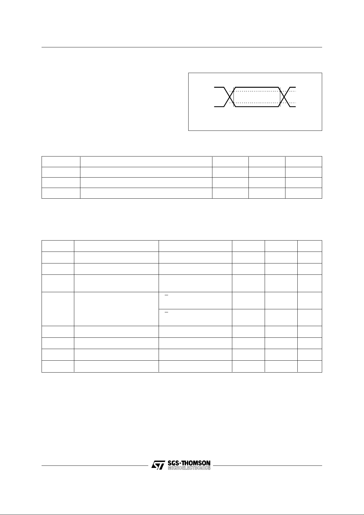
AC MEASUREMENT CONDITIONS
Figure 4. AC T estin g Input Ou tput W avefo r ms
Input Rise and Fall Times ≤ 50ns
Input Pulse Voltages 0.2V
Input and Output Timing
Reference Voltages
Note that Output Hi-Z is defined as the point where data
0.3V
to 0.8V
CC
to 0.7V
CC
CC
CC
0.8V
0.2V
CC
CC
is no longer driven.
T able 3. Input Parameters
(1)
(TA = 25 °C, f = 1 MHz )
Symbol Parameter Min Max Unit
C
IN
C
IN
t
LPF
Note: 1. Sampled only , not 100% test e d.
Input Capacitance (D) 8 pF
Input Capacitance (other pins) 6 pF
Input Signal Pulse Width 10 ns
T ab le 4. DC Characteristics
(T
= 0 to 70°C or –40 to 85°C; VCC = 3V to 5.5V)
A
0.7V
0.3V
AI00825
CC
CC
Symbol Parameter Test Condition Min Max Unit
I
LI
I
LO
I
CC
I
CC1
V
IL
V
IH
V
OL
V
OH
Input Leakage Current 2 µA
Output Leakage Current ±2 µA
VCC Supply Current (Active)
C = 0.1 V
@ 1 MHz, Q = Open
S = VCC, VIN = VSS or VCC,
VCC Supply Current (Standby)
S = VCC, VIN = VSS or VCC,
Input Low Voltage – 0.3 0.3 V
Input High Voltage 0.7 V
Output Low Voltage IOL = 2mA 0.2 V
Output High Voltage IOH = –2mA 0.8 V
V
V
= 5.5V
CC
CC
/0.9 VCC ,
CC
= 3V
CC
CC
2mA
50 µA
10 µA
CC
V
VCC + 1 V
CC
V
V
4/16
Page 5

ST95P04
Table 5. AC Characteristics
= 0 to 70°C or –40 to 85°C; VCC = 3V to 5.5V)
(T
A
Symbol Alt Parameter Test Condition Min Max Unit
f
C
t
SLCH
t
CLSH
t
CH
t
CL
t
CLCH
t
CHCL
t
DVCH
t
CHDX
t
DLDH
t
DHDL
t
HXCH
t
CLHX
t
SHSL
t
SHQZ
t
QVCL
t
CLQX
t
QLQH
t
QHQL
t
HHQX
t
HLQZ
(1)
t
W
Note: 1. Not enough characterisation data were available on this parameter at the time of issue this Data Sheet. The typical value is well
below 5ms, the maximum value will be reviewed and lowered when sufficient data is available.
t
t
t
t
t
t
t
DSU
t
t
t
HSU
t
t
t
t
t
t
t
t
f
SU
SH
WH
WL
RC
FC
DH
t
HH
CS
DIS
t
HO
RO
FO
HZ
t
C
Clock Frequency D.C. 1 MHz
S Setup Time 100 ns
S Hold Time 100 ns
Clock High Time 400 ns
Clock Low Time 400 ns
Clock Rise Time 1 µs
Clock Fall Time 1 µs
Data In Setup Time 100 ns
Data In Hold Time 100 ns
RI
FI
Data In Rise Time 1 µs
Data In Fall Time 1 µs
HOLD Setup Time 100 ns
HOLD Hold Time 100 ns
S Deselect Time 400 ns
Output Disable Time 300 ns
V
Clock Low to Output Valid 400 ns
Output Hold Time 0 ns
Output Rise Time 150 ns
Output Fall Time 150 ns
LZ
HOLD High to Output Low-Z 300 ns
HOLD Low to Output High-Z 300 ns
W
Write Cycle Time 10 ms
5/16
Page 6

ST95P04
Figure 5. Output Timing
S
C
tCLQX
tQVCL
tCH
tCL
tSHQZ
Q
D
ADDR.LSB IN
MSB OUT MSB-1 OUT LSB OUT
Figure 6. Serial Input Timing
S
C
tDVCH
tSLCH
tQLQH
tQHQL
AI01070B
tSHSL
tCLSH
tCHCL
6/16
tCHDX
D
Q
MSB IN
HIGH IMPEDANCE
tCLCH
LSB IN
tDLDH
tDHDL
AI01071
Page 7

Figure 7. Hold Timing
S
C
Q
D
HOLD
tCLHX
ST95P04
tHXCH
tHXCH
tCLHX
tHHQXtHLQZ
AI01072B
Write Protect (
protect. When
W). This pin is for hardware write
W is low, non-volatile writes to the
ST95P04 are disabled but any other operation
stays enabled. When
including non-volatile writes are available.
W is high, all operations
W going
low at any time before the last bit D0 of the data
stream will reset the write enable latch and prevent
programming. No action on
W or on the write
enable latch can interrupt a write cycle which has
commenced.
HOLD). The HOL D pin is used to pause
Hold (
serial communications with a ST95P04 without
resetting the serial sequence. To take the Hold
condition into account, the product must be selected (
a high to low transition on
resume the communications,
S = 0). Then the Hold state i s validated by
HOLD when C is low. To
HOLD is brought high
when C is low. During Hold condition D, Q, and C
are at a high impedance state.
When the ST95P04 is under Hold condition, it is
possible to deselect it. However , the serial communications will remain paused after a reselect, and
the chip will be reset.
OPERATIONS
All instructions, addresses and data are shifted in
and out of the chip MSB first. Data input (D) is
sampled on the first rising edge of clock (C) after
the chip select (
S) goes low . Prior to any operation,
a one-byte instruction code m ust be entered in t he
chip. This code is entered via the data input (D),
and latched on the rising edge of the clock input
(C). T o enter an instruc tion code, the product must
have been previously selected (
S = low). Table 7
shows the instruction set and format for device
operation. When an invalid instruction is sent (one
not contained in T able 7), the chip is automatically
deselected. For ope rations that read or wri te data
in the memory array, bit 3 of the instruction is the
MSB of the address, otherwise, it is a don’t care.
Write En able (WR EN) an d Wr ite Disab le (W RDI)
The ST95P04 contains a write enable latch. This
latch must be set prior to every WRITE or WRSR
operation. The WREN instruction will set the latch
and the WRDI instruction will reset the latch. The
latch is reset under all the following conditions:
W pin is low
–
– Power on
– WRDI instruction executed
– WRSR instruct ion executed
– WRITE instruct ion executed
As soon as the WREN or WRDI instruction is
received by the ST95P04, the circuit executes the
instruction and enters a wait mode until it is deselected.
7/16
Page 8

ST95P04
Read Status Regist er (RDSR)
The RDSR instruct ion provides access to the status
register. The status register may be read at any
time, even during a non-volatile write. As soon as
the 8th bit of the status register is read out, the
ST95P04 enters a wait mode (data on D are not
decoded, Q is in Hi-Z) until it is deselected.
The status register form at is as follows:
b7 b0
1 1 1 1 BP1 BP0 WEL WIP
BP1, BP0: Read and Write bits
WEL, WIP: Read only bits.
During a non-volatile writ e to the memor y array, all
bits BP1, BP0, WE L, WIP are valid and can be read.
During a non volatile write to the status register, th e
only bits WE L and WIP are valid and can be read.
The values of BP1 and BP0 read at that time
correspond to the previous contents of the status
register.
The Writ e-In- Process ( WIP ) read only bit i ndicates
whether the ST95P04 is busy with a write operation. When set to a ’1’ a write is in progress, when
set to a ’0’ no write is in progress.
The Write Enable Latch (WEL) read only bit in dicates the status of the write enable latch. When set
to a ’1’ the latc h is set, when s et to a ’ 0’ the latc h is
reset.
The Block Protect (BP0 and BP1) bits indicate the
extent of the protection employed. These bits are
set by the user issuing the WRSR instruction.
These bits are non-volatile.
Write Status Register (WRSR)
The WRSR instruction allows the user to select the
size of protected m emory. The ST95P04 is divided
into four 1024 bit blocks. The user may read the
blocks but will be unable to write within the select ed
blocks.
The blocks and respective WRSR control bits are
shown in Table 6.
When the WRSR instruction and the 8 b its of the
Status Register are latched-in, the internal write
cycle is then triggered by the rising edge of
rising edge of
S must appear after th e 8th b it of the
S. This
Status Register content (it must not appear a 17th
clock pulse before the rising edge of
S), otherwise
the internal write sequence is not performed.
Read Operation
The chip is first select ed by putting
S low. The serial
one byte read instruction is followed by a one byte
address (A7-A0), each bit being latched-in during
the rising edge of the clock (C). Bit 3 of the read
instruction contains address A8 (most significant
address bit). This bit is used to select the first or
second page of the device. Then, the data stored
in the memory at the selected address is shifted out
on the Q output pin; each bit being shifted out
during the falling edge of the clock (C). The data
stored in the memory at the next address can be
read in sequence by continuing to provide clock
T able 6. Array Addresses Protect
Status Register Bits
BP1 BP0
0 0 non e
0 1 180h - 1FFh
1 0 100h - 1FFh
1 1 000h - 1FFh
Array Addresses
Protected
T ab le 7. Instruction Set
Instruction Description Instruction Format
WREN Set Write Enable Latch 0000 X110
WRDI Reset Write Enable Latch 0000 X100
RDSR Read Status Register 0000 X101
WRSR Write Status Register 0000 X001
READ Read Data from Memory Array 0000 A01 1
WRITE Write Data to Memory Array 0000 A010
Notes: A = 1, Upper page selected
A = 0, Lower page selected
X = Don’t care
8/16
Page 9

ST95P04
pulses. The byte address is automatically incremented to the next higher address after each byte
of data is shifted out. When the highest address is
reached (1FFh), the address counter rolls over to
0h allowing the read cycle to be continued indefinitely. The read operation is terminated by deselecting the chip. T he chip c an be deselected at any
time during data output. Any read attempt during a
non-volatile write cycle will be rejected and will
deselect the chip.
Byte Write Operation
Prior to any write attempt, the write enable latch
must have been set by issuing the WREN instruction. First, the device is selected (
S = low) and a
serial WREN instruction byte is issued. Then, the
product is deselected by taking
S high. After the
WREN instruction byte is sent, the ST95P04 will
set the write enable latch and then remain in
standby until it is deselected. Then, the write stat e
is entered by selecting the chip, issuing a one byt e
address (A7-A0), and one byte of data. Bit 3 of the
write instruct ion contains address A8 (most significant address bit).
S must remain low for the entire
duration of the operation. The product must be
deselected just after the eigth bit of data has been
latched in. If not, the write process is cancelled. As
soon as the product is deselected, the self-timed
write cycle is initiated. While the write is in progress,
the status re gister may be read to c heck BP1, B P0,
WEL and WIP. WIP is high during the self-timed
write cycle. When the cycle is close to c ompletion,
the write enable latch is reset.
Page Write Operation
A maximum of 16 bytes of data may be written
during one non-volatile write cycle. All 16 bytes
must reside on the same page. The page write
mode is the same as the byte write mode except
that instead of deselecting after the first byte of
data, up to 15 additional bytes can be shifted in
prior to deselecting the chip. A page address begins
with address xxxx 0000 and ends with xxxx 1111.
If the address counter reaches xxxx 1111 and the
clock continues, the counter will roll over to the first
address of the page (xxxx 0000) and overwrite any
previous written data. The pro gramming cycle will
only start if the
S transition does occur at the clock
low pulse just after the eigth bit of data of a word is
received.
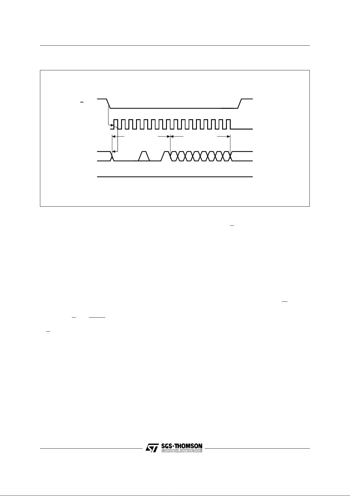
Figure 8. Read Operation Sequence
S
21 345678910111213141516171819A20 21 22 23
0
C
INSTRUCTION BYTE ADDRESS
D
HIGH IMPEDANCE
Q
DATA OUT
7 65432 0
MSB
1
AI01066
9/16
Page 10

ST95P04
Figure 9. Write Enable Latch Seq uence
S
C
D
Q
21 34567
0
HIGH IMPEDANCE
AI01067
Figure 10. Write Op erati on Seq uen c e
S
21 34567891011121314151617181920 21 22 23
0
C
INSTRUCTION BYTE ADDRESS
D
HIGH IMPEDANCE
Q
A
DATA BYTE
7 65432 0
1
AI01068
10/16
Page 11

Figure 1 1. Page W rit e Operati on Seq uen ce
S
21 34567891011121314151617181920 21 22 23
0
C
ST95P04
INSTRUCTION BYTE ADDRESS
D
S
C
D
7 6 321054
A
2625 27 28 29 30 31
DATA BYTE 2
8+8N
9+8N
10+8N
11+8N
12+8N
13+8N
14+8N
DATA BYTE N
7
6 3210247 65432
5 4
DATA BYTE 1
140
1
141
1
7 65432 0
15+8N
136
137
138
139
DATA BYTE 16
142
7
143
0
AI01069
Figure 12. RDSR: Read Statu s Register Seq u ence
S
21 3456789101112131415
0
C
INSTRUCTION
D
Q
HIGH IMPEDANCE
STATUS REG. OUT
7 6543210
MSB
AI01433
11/16
Page 12
ST95P04
Figure 13. WRSR: W rite St atu s Regi ster Seq uen c e
S
21 3456789101112131415
0
C
INSTRUCTION STATUS REG.
D
HIGH IMPEDANCE
Q
AI01434
POWER ON STA TE
After a Power up the ST95P04 is in the following
state :
– The device is in the low power standby state.
– The chip is deselected.
– The chip is not in hold condition.
– The write enable latch is reset.
– BP1 and BP0 are unchanged (non-volatile
bits).
DATA PROTECTION AND PROTOCOL SAFETY
– All inputs are protected against noise, see Ta-
ble 3.
– Non valid
S and HOLD trans itions are not
taken into account.
S must come high at the proper clock count in
–
order to start a non-volatile write cycle (in the
memory array or in the cycle status register).
The Chip Select
S must rise during the clock
pulse following the introduction of a multiple of
8 bits.
– Access to the memory array during non-vola-
tile programming cycle is cancelled and the
chip is automatically deselected; however, the
programming cycle continues.
– After either of the following operations
(WREN, WRDI , RDSR) is complet ed, the chi p
enters a wait state and waits for a deselect.
– The write enable latch is reset upon power-up.
– The write enable latch is reset when
W is
brought low.
INITIAL DELIVERY STATE
The device is delivered with the memory array in a
fully erased state (all data set at all "1’s" or FFh).
The block protect bits are initialized to 00.
12/16
Page 13

ORDERING INFORMATION SCHEME
Example: ST95P04 M 6 TR
ST95P04
Data Strobe
P * D Q
Notes: P * Data In strobed on rising edge of the clock (C) and Data Out synchronized from the falling edge of the clock.
3 * Temperature range on special request only.
Package
B PSDIP8
0.25 mm Frame
M SO8
1501mil Width
Temperature Range
1 0 to 70 °C
6 –40 to 85 °C
3 * –40 to 125 °C
Option
TR Tape & Reel
Packing
For a list of available options (Package, T emperatur e Range, etc...) refer to the current Memory Shor tform
catalogue.
For further information on any aspect of this device, please contact the SGS-THOMSON Sales Office
nearest to you.
13/16
Page 14
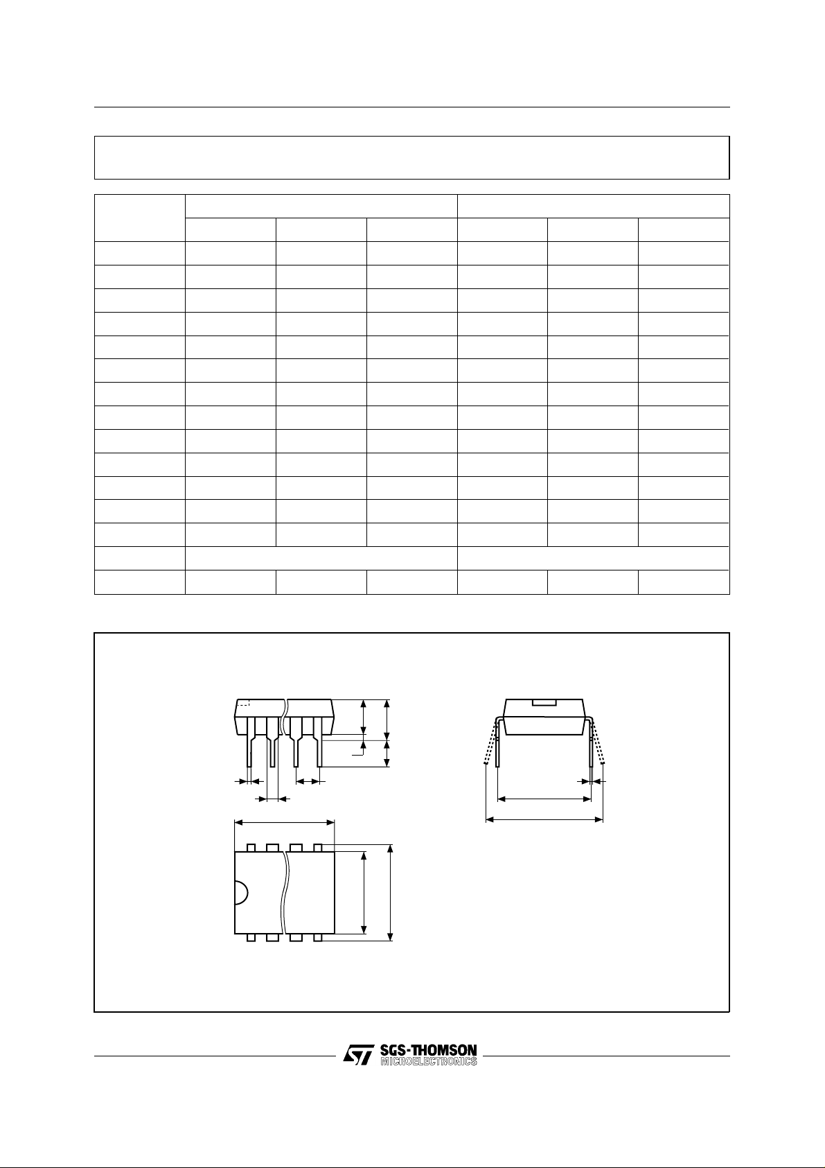
ST95P04
PSDIP8 - 8 pin Plastic Skinny DIP, 0.25mm lead frame
Symb
Typ Min Max Typ Min Max
A 3.90 5.90 0.154 0.232
A1 0.49 – 0.019 –
A2 3.30 5.30 0.130 0.209
B 0.36 0.56 0.014 0.022
B1 1.15 1.65 0.045 0.065
C 0.20 0.36 0.008 0.014
D 9.20 9.90 0.362 0.390
E 7.62 – – 0.300 – –
E1 6.00 6.70 0.236 0.264
e1 2.54 – – 0.100 – –
eA 7.80 – 0.307 –
eB 10.00 0.394
L 3.00 3.80 0.118 0.150
N8 8
CP 0.10 0.004
PSDIP8
mm inches
Drawing is not to scale
14/16
A2
A1AL
B
e1
B1
D
N
C
eA
eB
E1 E
1
PSDIP-a
Page 15

SO8 - 8 lead Plastic Small Outline, 150 mils body width
ST95P04
Symb
Typ Min Max Typ Min Max
A 1.35 1.75 0.053 0.069
A1 0.10 0.25 0.004 0.010
B 0.33 0.51 0.013 0.020
C 0.19 0.25 0.007 0.010
D 4.80 5.00 0.189 0.197
E 3.80 4.00 0.150 0.157
e 1.27 – – 0.050 – –
H 5.80 6.20 0.228 0.244
h 0.25 0.50 0.010 0.020
L 0.40 0.90 0.016 0.035
α 0° 8° 0° 8°
N8 8
CP 0.10 0.004
SO8
mm inches
Drawing is not to scale
B
SO-a
h x 45˚
A
C
e
CP
D
N
E
H
1
LA1 α
15/16
Page 16

ST95P04
Information furnished is b elieved to be accurate and reliable. Howe ver, SGS-THOMSON Microelectronics assumes no responsibility for the
consequences of use of such information nor for any infringement of patents or other rights of third parties which may result from its use. No
license is granted by implication or otherwise under any patent or patent rights of SGS-THOMSON Microelectronics. Specificat ions mentioned
in this publication are subject to change without notice. This publication supersedes and replaces all information previously supplied.
SGS-THOMSON Microelectronics products are not authorized for use as critical components in life support devices or systems without express
written approval of SGS-THOMSON Microelectronics.
© 1996 SGS-THOMSON Microelectronics - All Rights Reserved
Australia - Brazil - China - France - Germany - Hong Kong - Italy - Japan - Korea - Malaysia - Malta - Morocco - Th e Netherlands -
Singapore - Spain - Sweden - Switzerland - Taiwan - Thailand - United Kingdom - U.S.A.
SGS-THOMSON Microelectronics GROUP OF COMPANIES
16/16
Page 17

 Loading...