

Page 1
CD4047BC
Low Power Monostable/Astable Multivibrator
CD4047BC Low Power Monostable/Astable Multivibrator
October 1987
Revised May 1999
General Description
The CD4047B is capable of operating in either the
monostable or astable mode. It requires an external capacitor (between pins 1 and 3) and an external resistor
(between pins 2 and 3) to determine the output pulse width
in the monostable mode, an d the output frequency in the
astable mode.
Astable operation i s ena bl ed b y a hi gh level on the astable
input or low level on the astable
quency (at 50% duty cycle) at Q and Q
mined by the timing c omponents. A frequency tw ice that of
Q is available at the Oscillator Outp ut; a 50 % duty cyc le is
not guaranteed.
Monostable operati on is obtained when t he device is triggered by LOW-to-HIGH transition at + trigger input or
HIGH-to-LOW transition at − trigger input. The device can
be retriggered by applying a simulta neous LOW-to-HIGH
transition to both the + trigger and retrigger inputs.
A high level on Reset input resets the outputs Q to LOW, Q
to HIGH.
input. The output fre-
outputs is deter-
Features
■ Wide supply voltage range: 3.0V to 15V
■ High noise immunity: 0.45 V
■ Low power TTL compatibility: Fan out of 2 driving 74L
or 1 driving 74LS
SPECIAL FEATURES
■ Low power consumption: special CMOS oscillator
configuration
■ Monostable (one-shot) or astable (free-running)
operation
DD
(typ.)
■ True and complemented buffered outputs
■ Only one external R and C required
MONOSTABLE MULTIVIBRATOR FEATURES
■ Positive- or negative-edge trigger
■ Output pulse width independent of trigger pulse duration
■ Retriggerable option for pulse width expansion
■ Long pulse widths poss ible u sing s mall RC c ompon ent s
by means of external counter provision
■ Fast recovery time essentially independent of pulse
width
■ Pulse-width accuracy maintained at duty cycles
approaching 100%
ASTABLE MULTIVIBRATOR FEATURES
■ Free-running or gatable operating modes
■ 50% duty cycle
■ Oscillator output available
■ Good astable frequency stability
typical= ±2% + 0.03%/°C @ 100 kHz
frequency= ±0.5% + 0.015% /°C @ 10 kHz
deviation (circuits trimmed to frequency V
±10%)
= 10V
DD
Applications
• Frequency discriminators
• Timing circuits
• Time-delay applications
• Envelope detection
• Frequency multiplication
• Frequency division
Ordering Code:
Order Number Package Number Package Description
CD4047BCM M14A 14-Lead Small Outline Integrated Circuit (SOIC), JEDEC MS-120, 0.150” Narrow
CD4047BCN N14A 14-Lead Plastic Dual-In-Line Package (PDIP), JEDEC MS-001, 0.300” Wide
Devices also availab le in Tape and Reel. Specify by appending th e s uffix let t er “X” to the ordering cod e.
© 1999 Fairchild Semiconductor Corporation DS005969.prf www.fairchildsemi.com
Page 2
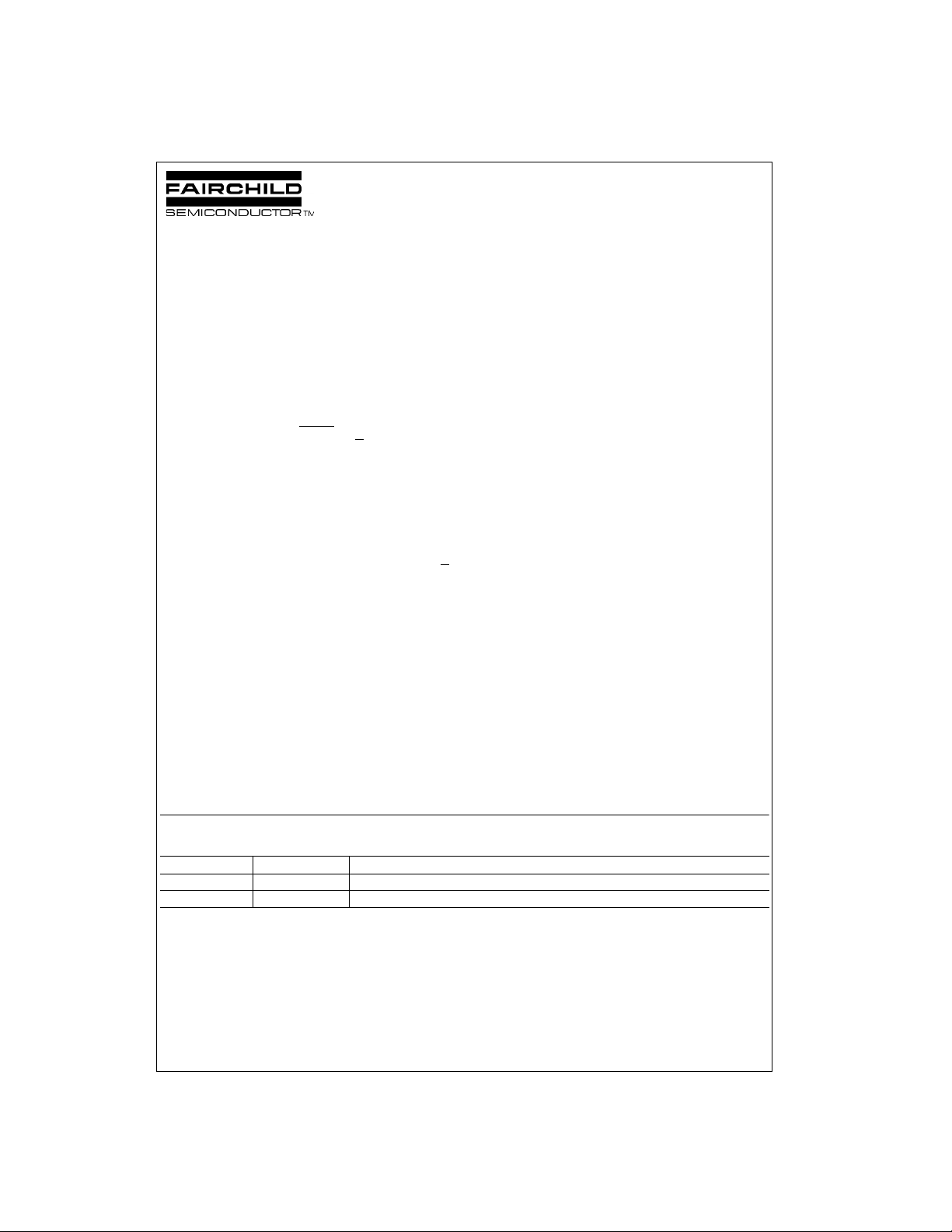
Connection Diagram
Pin Assignments for SOIC and DIP
CD4047BC
Top View
Function Table
Terminal Connections Output Pulse Typical Ou tput
Function
Astable Multivibrator
Free-Running 4, 5, 6, 14 7, 8, 9, 12 10, 11, 13 t
True Gating 4, 6, 14 7, 8, 9, 12 5 10, 11, 13 t
Complement Gating 6, 14 5, 7, 8, 9, 12 4 10, 11, 13
Monostable Multivibrator
Positive-Edge Trigger 4, 14 5, 6, 7, 9, 12 8 10, 11
Negative-Edge Trigger 4, 8, 14 5, 7, 9, 12 6 10, 11 t
Retriggerable 4, 14 5, 6, 7, 9 8, 12 10, 11
External Countdown (Note 1) 14 5, 6, 7, 8, 9, 12 Figure 1 Figure 1 Figure 1
Note 1: External re s is to r between terminals 2 a nd 3. External capacitor between terminals 1 and 3.
To V
DD
To V
SS
Input Pulse
To Pulse Width
From Period or
(10, 11) = 4.40 RC
A
(13) = 2.20 RC
A
(10, 11) = 2.48 RC
M
Typical Implementation of External Countdown Option
t
= (N − 1) tA + (tM + tA/2)
EXT
www.fairchildsemi.com 2
FIGURE 1.
Page 3
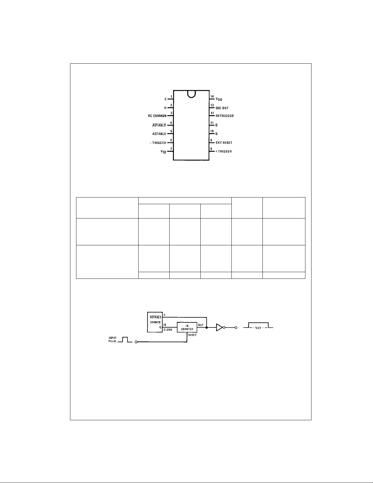
Block Diagram
Logic Diagram
CD4047BC
*Special input prote ction circuit to permit larger input-voltage swi ngs.
3 www.fairchildsemi.com
Page 4

Absolute Maximum Ratings(Note 2)
(Note 3)
DC Supply Voltage (VDD) −0.5V to +18V
Input Voltage (VIN) −0.5V to VDD+0.5V
CD4047BC
Storage Temperature Range (TS) −65°C to +150°C
Power Dissipation (P
)
D
Dual-In-Line 700 mW
Small Outline 500 mW
Lead Temperature (T
)
L
(Soldering, 10 seconds) 260°C
DC Electrical Characteristics (Note 3)
Symbol Parameter Conditions
I
Quiescent Device Current VDD = 5V 20 20 150 µA
DD
V
LOW Level Output Voltage |IO| < 1 µA
OL
V
HIGH Level Output Voltage |IO| < 1 µA
OH
V
LOW Level Input Voltage VDD = 5V, VO = 0.5V or 4.5V 1.5 2.25 1.5 1.5 V
IL
V
HIGH Level Input Voltage VDD = 5V, VO = 0.5V or 4.5V 3.5 3.5 2.75 3.5 V
IH
I
LOW Level Output Current VDD = 5V, VO = 0.4V 0.52 0.44 0.88 0.36 mA
OL
(Note 4) VDD = 10V, VO = 0.5V 1.3 1.1 2.25 0.9 mA
I
HIGH Level Output Current VDD = 5V, VO = 4.6V −0.52 −0.44 −0.88 −0.36 mA
OH
(Note 4) VDD = 10V, VO = 9.5V −1.3 −1.1 −2.25 −0.9 mA
I
Input Current VDD = 15V, VIN = 0V −0.3 −10−5−0.3 −1.0 µA
IN
Note 4: IOH and IOL are tested one output at a time.
VDD = 10V 40 40 300 µA
VDD = 15V 80 80 600 µA
VDD = 5V 0.05 0 0.05 0.05 V
VDD = 10V 0.05 0 0.05 0.05 V
VDD = 15V 0.05 0 0.05 0.05 V
VDD = 5V 4.95 4.95 5 4.95 V
VDD = 10V 9.95 9.95 10 9.95 V
VDD = 15V 14.95 14.95 15 14.95 V
VDD = 10V, VO = 1V or 9V 3.0 4.5 3.0 3.0 V
VDD = 15V, VO = 1.5V or 13.5V 4.0 6.75 4.0 4.0 V
VDD = 10V, VO = 1V or 9V 7.0 7.0 5.5 7.0 V
VDD = 15V, VO = 1.5V or 13.5V 11.0 11.0 8.25 11.0 V
VDD = 15V, VO = 1.5V 3.6 3.0 8.8 2.4 mA
VDD = 15V, VO = 13.5V −3.6 −3.0 −8.8 −2.4 mA
VDD = 15V, VIN = 15V 0.3 10−50.3 1.0 µA
Recommended Operating
Conditions
DC
DC Supply Voltage (V
DC
Input Voltage (VIN)0 to V
Operating Temperature Range (TA) −40°C to +85°C
Note 2: “Absolute Maximum Ratings” ar e those value s beyond which the
safety of the device cannot be guaranteed. They are not meant to imply
that the devices should b e operate d at thes e limits. T he table of “Recommended Operating Conditions” and “Electrical Characteristics” provides
conditions for actua l device operation.
= 0V unless otherw is e s pecified.
Note 3: V
SS
−40°C25°C85°C
Min Max Min Typ Max Min Max
(Note 3)
) 3V to 15V
DD
DC
DD VDC
Units
www.fairchildsemi.com 4
Page 5

AC Electrical Characteristics (Note 5)
= 25°C, CL = 50 pF, RL = 200k, input tr = tf = 20 ns, unless otherwise specified.
T
A
Symbol Parameter Conditions Min Typ Max Units
t
, t
PHL
PLH
t
, t
PHL
PLH
t
, t
PHL
PLH
t
, t
PHL
PLH
t
, t
PHL
PLH
t
, t
THL
TLH
tWL, t
WH
t
, t
RCL
FCL
C
IN
Note 5: AC Parameters are guaranteed by DC c orrelated testing.
Propagation Delay Time Astable, VDD = 5V 200 400 ns
Astable to Osc Out
VDD = 10V 100 200 ns
VDD = 15V 80 160 ns
Astable, Astable to Q, Q
VDD = 5V 550 900 ns
VDD = 10V 250 500 ns
VDD = 15V 200 400 ns
+ Trigger, − Trigger to Q
VDD = 5V 700 1200 ns
VDD = 10V 300 600 ns
VDD = 15V 240 480 ns
+ Trigger, Retrigger to Q
VDD = 5V 300 600 ns
VDD = 10V 175 300 ns
VDD = 15V 150 250 ns
Reset to Q, Q
VDD = 5V 300 600 ns
VDD = 10V 125 250 ns
VDD = 15V 100 200 ns
Transition Time Q, Q, Osc Out
VDD = 5V 100 200 ns
VDD = 10V 50 100 ns
VDD = 15V 40 80 ns
Minimum Input Pulse Duration Any Input
VDD = 5V 500 1000 ns
VDD = 10V 200 400 ns
VDD = 15V 160 320 ns
+ Trigger, Retrigger, Rise and VDD = 5V 15 µs
Fall Time VDD = 10V 5 µs
VDD = 15V 5 µs
Average Input Capacitance Any Input 5 7.5 pF
CD4047BC
5 www.fairchildsemi.com
Page 6

Typical Performance Characteristics
, Osc Out Period Accuracy vs
CD4047BC
Typical Q, Q
Supply Voltage (Astable Mode Operation)
Typical Q, Q, Pulse Width Accuracy vs
Supply Voltage Monostable Mode Operation
fQ, Q RC
A 1000 kHz 22k 10 pF
B 100 kHz 22k 100 pF
C 10 kHz 220k 100 pF
D 1 kHz 220k 1000 pF
E 100 Hz 2.2M 1000 pF
Typical Q, Q
vs Temperature Astable Mode Operation
A 1000 kHz 22k 10 pF
B 100 kHz 22k 100 pF
C 10 kHz 220k 100 pF
D 1 kHz 220k 1000 pF
and Osc Out Period Accuracy
fQ, Q RC
t
M
A 2 µs 22k 10 pF
B 7 µs 22k 100 pF
C 60 µs 220k 100 pF
D 550 µs 220k 1000 pF
E 5.5 ms 2.2M 1000 pF
Typical Q and Q Pulse Width Accuracy vs
Temperature Monostable Mode Ope r ation
t
M
A 2 µs 22k 10 pF
B 7 µs 22k 100 pF
C 60 µs 220k 100 pF
D 550 µs 220k 1000 pF
RC
RC
www.fairchildsemi.com 6
Page 7

Timing Diagrams
Astable Mode Monostable Mode
CD4047BC
Retrigger Mode
7 www.fairchildsemi.com
Page 8

Physical Dimensions inches (millimeters) unless otherwise noted
CD4047BC
14-Lead Small Outline Integrated Circuit (SOIC), JEDEC MS-120, 0.150” Narrow
Package Number M14A
www.fairchildsemi.com 8
Page 9

Physical Dimensions inches (millimeters) unless otherwise noted (Continued)
CD4047BC Low Power Monostable/Astable Multivibrator
14-Lead Plastic Dual-In-Line Package (PDIP), JEDEC MS-001, 0.300” Wide
LIFE SUPPORT POLICY
FAIRCHILD’S PRODUCTS ARE NOT AUTHORIZED FOR USE AS CRITICAL COMPONENTS IN LIFE SUPPORT
DEVICES OR SYSTEMS WITHOUT THE EXPRESS WRITTEN APPROVAL OF THE PRESIDENT OF FAIRCHILD
SEMICONDUCTOR CORPORATION. As used herein:
1. Life support devices or systems are devices or systems
which, (a) are intended for surgical implant into the
body, or (b) support or sustain life, and (c) whose failure
to perform when properly used in accordance with
instructions for use provide d in the labe l ing, can be re asonably expected to result in a significant injury to the
user.
Package Number N14A
2. A critical componen t in any com ponen t of a life s upport
device or system whose failu re to perform can b e reasonably expected to cause the failure of the life support
device or system, or to affect its safety or effectiveness.
www.fairchildsemi.com
Fairchild does not assume any responsibility for use of any circuitry described, no circuit patent licenses are implied and Fairchild reserves the right at any time without notice to change said circuitry and specifications.
 Loading...