

Page 1
• HIGH GAIN Gp = 21 dB at 1.85 GHz
• LOW NOISE FIGURE NF = 1.3 dB at 1.85 GHz
• LOW CURRENT CONSUMPTION 5.9 mA
• OPEN COLLECTOR OUTPUT
• TYPICAL SUPPLY VOLTAGE: 2.4-3 V
• GAIN-STEP-MODE (36dB)
• ULTRA MINIATURE SOT323-6L PACKAGE (LEAD
FREE)
APPLICATIONS
• LNA FOR CELLULAR MARKET (ideal for GSM900,
DCS1800 and PCS1900).
• LNA FOR GPS APPLICATIONS
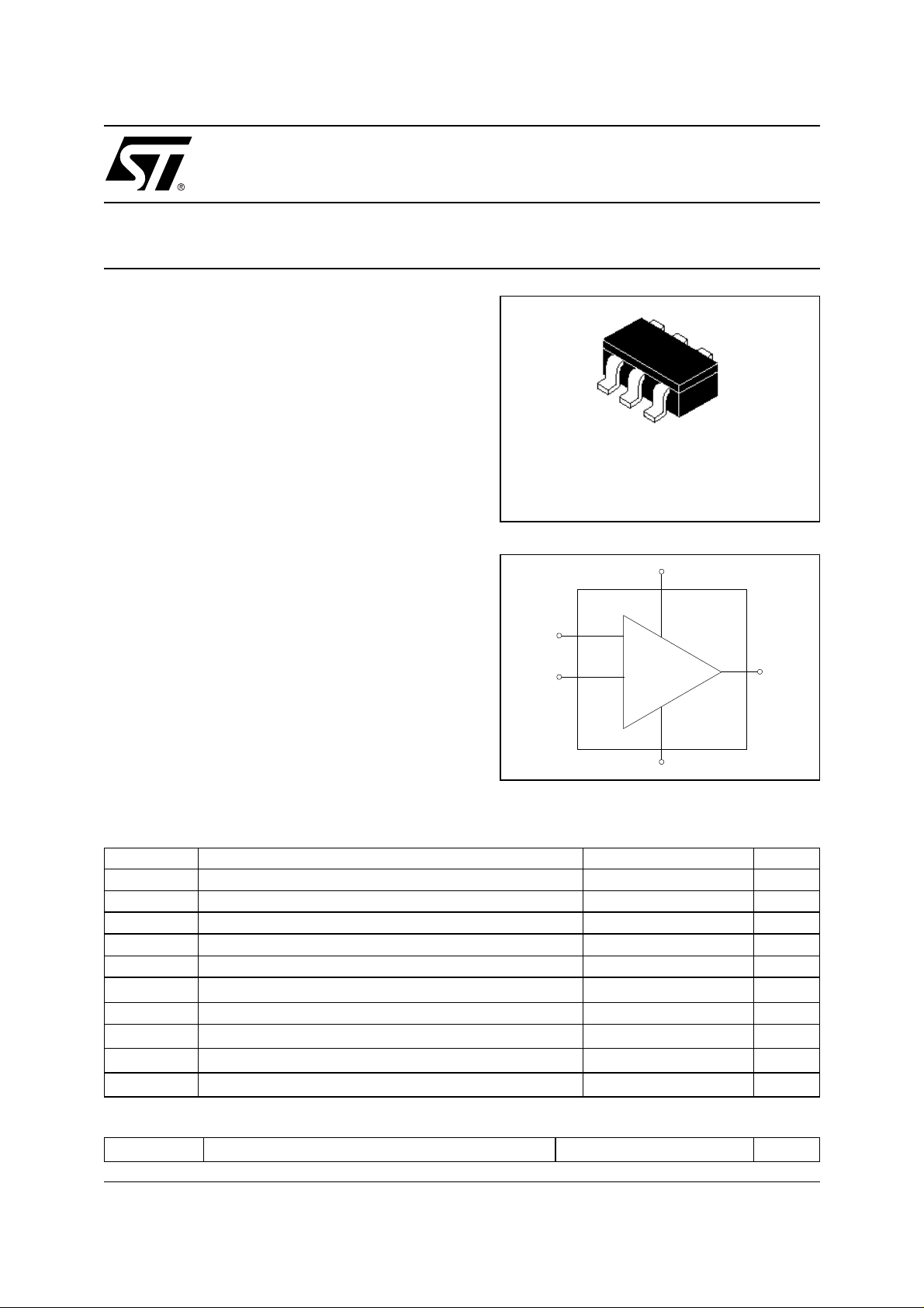
SMA428A
High Gain, Low Noise Amplifier
PRELIMINARY DATA
SOT323-6L (SC70)
ORDER CODE
SMA428ATR
BLOCK DIAGRAM
Vcc, 1
BRANDING
TBD
DESCRIPTION
GS, 4
High gain and low noise figures make the SMA428A an
ideal solution for Low Noise Amplifiers and receiver
front end stages up to 2.5 GHz. SMA428A’s typical
In, 6
supply voltage range is 2.4 to 3.3 volts. It shows
excellent performances in terms of NF, Gain and
current consumption, using just 3 external matching
components. Applying supply voltage to the GS pin and
grounding Vcc pin, it provides a reduced gain step of 35
dB. SMA428A is hou se d in ul tra miniature S OT323-6L
GND, 2;5
package(LEAD FREE), the relative dimensions are
1.15mmx1.8mm with 0.8mm thickness.
ABSOLUTE MAXIMUM RATINGS
Symbol Parameter Value Unit
V
cc
V
out
V
GS
I
tot
I
in
P
tot
P
IN
T
op
T
stg
T
j
Device voltage 4 V
Voltage at pin Out 4 V
Voltage at pin GS 3.5 V
Total Device Current 12 mA
Current into pin In 0.5 mA
Total dissipation, Ts < 125 oC
Input Power 8 dBm
Operating temperature -40 to +85
Storage temperature -65 to +150
Max. operating junction temperature 150
60 mW
Out, 3
o
C
o
C
o
C
THERMAL RESISTANCE
R
thjs
March, 10 2003
Thermal Resistance Junction soldering point 200
o
C/W
1/8
Page 2
SMA428A
Test Circuit (Fig. 1)
Typical application circuit (Fig. 2)
V
V
CTRL
CTRL
3 kΩ
3 kΩ
100 pF
RF in
RF in
100 pF
GS
GS
In
In
Vcc
Vcc
SMA428A
SMA428A
GND
GND
Out
Out
180 pF47 pF
180 pF47 pF
6.8 nH
6.8 nH
0.5 pF
0.5 pF
Supply
Supply
RF Out
RF Out
2/8
Page 3
SMA428A
ELECTRICAL CHARACTERISTICS
(Ta = +25
Symbol Parameters Test Conditions Min Typ Max Unit
P
o
C, VCC = 2.7V, tested in circuit shown in fig.1, unless otherwise specified)
f Frequency Range 1850 MHz
I
Gp
NF
-1dB
IIP3 Input third order intercept point -13 dBm
L
I
CTR
Total device current 5.9 7.5 mA
tot
Power Gain 18 21 dB
Noise Figure (Zs = 50 Ω)
Input Power at 1 dB Gain Compression -23 dBm
Insertion Loss in Gain-Step-Mode
GS
Current consumption in Gain-Step-Mode
Vcc = 0.0 V, V
R
CTRL
Vcc = 0.0 V, V
R
CTRL
CTRL
= 3 kΩ
CTRL
= 3 kΩ
= 2.7 V,
= 2.7 V,
1.3 1.7 dB
11 18 dB
0.33 mA
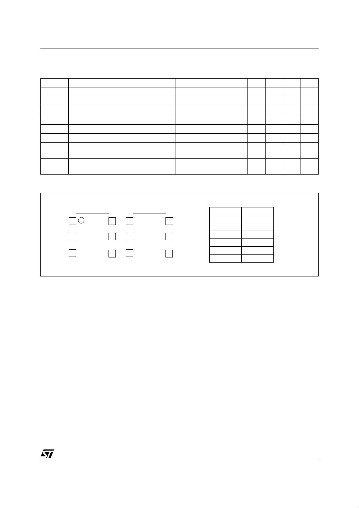
PIN CONNECTION
(Top View)
1
2
3
6
5
4
(Botto m View)
6
5
4
Pin No. Pin Name
1
2
3
1VCC
2GND
3OUTPUT
4GS
5GND
6INPUT
3/8
Page 4

SMA428A
S-Parameters ( Z
24
23
22
21
Gp (dB)
20
19
18
1800 1810 1820 1830 1840 1850 1860 1870 1880 1890 1900
-20
-22
-24
-26
-28
-30
ISL (dB)
Tc = 25 °C
-32
-34
-36
-38
-40
1800 1810 1820 1830 1840 1850 1860 1870 18 80 1890 190 0
= 50 Ω, VCC = 2.7V, measured in application circuit shown in fig.2)
L = ZS
Tc = 25 °C
Tc = -40 °C
Tc = 85 °C
f (MHz)
Tc = -40 °C
Tc = 85 °C
f ((MHz)
0
-1
-2
-3
Tc = 85 °C
-4
-5
IRL (dB)
-6
-7
-8
-9
-10
1800 1810 1820 1830 1840 1850 1860 1870 1880 1890 1900
10
5
0
-5
-10
-15
ORL (dB)
-20
-25
-30
-35
-40
1800 1810 1820 1830 1840 1850 1860 187 0 1880 1890 1900
Tc = -40 °C
Tc = 85 °C
Tc = 25 °C
f (MHz)
Tc = -40 °C
Tc = 25 °C
f (MHz )
4/8
Page 5

TYPICAL PERFORMANCE
Supply Current Vs Temperature
SMA428A
Control Current Vs Temperature
0
-5
-10
-15
Gp (dB)
-20
-25
-30
1800 1810 18 20 1830 1840 1850 1 860 1870 1880 18 90 1900
OFF-Gain
-10
-12
-14
-16
-18
-20
Gp (dB)
-22
-24
-26
-28
-30
(Vcc = 0V, Vctrl = 2.7V, Rctrl = 3Kohm)
1800 1810 18 20 1830 1840 185 0 186 0 1870 1880 18 90 190 0
Tc = 25 °C
Tc = 85 °C
Tc = -40 °C
f (MHz)
Tc = 25 °C
Tc = 85 °C
Tc = -40 °C
f (MHz)
0.5
0.45
0.4
0.35
0.3
0.25
Ictrl (mA)
0.2
0.15
0.1
0.05
0
-40 -25 25 50 85
T (°C)
5/8
Page 6

SMA428A
TAPE & REEL DIMENSIONS
mm
MIN. TYP. MAX
A 178.5 179 179.5
C 12.8 13.0 13.5
D 20.2
N 54.5 55 55.5
T 14.4
Ao 2.25
Bo 2.7
Ko 1.2
Po 3.8 (cumulative 10 Po) 4.0 4.2 (cumulative 10 Po)
P 4.0
DEVICE ORIENTATION
6/8
TOP VIEW END VIEW
428428428
428
Page 7

SMA428A
SOT323-6L MECHANICAL DA TA
mm Inch
DIM.
A 0.8 1.1 0.031 0.043
A1 0 0.1 0 0.004
A2 0.8 1 0.0031 0.039
b 0.15 0.3 0.006 0.012
c 0.1 0.18 0.004 0.007
D 1.8 2.2 0.071 0.088
E 1.15 1.35 0.045 0.59
e 0.65 0.025
H 1.8 2.4 0.071 0.094
Q 0.1 0.4 0.004 0.016
MIN. TYP. MAX MIN. TYP. MAX
7/8
Page 8

SMA428A
p
Information furnished is believed to be ac curate and reli able. Howev er, STMicroel ectronics assumes no responsibilit y for the consequ ences
of use of such information nor for any infringement of patents or other rights of third parties which may result from its use. No license is granted
by implic ation or otherwise under any patent or patent rights of STMi croelectr onics. Specifications mentioned in thi s publicati on are sub j ect
to change without notice. This publication supersedes and replaces all information previously supplied. STMicroelectronics products are not
authorized for use as cri tical comp onents in life support dev i ces or systems wi t hout express written ap proval of STMi croelect roni cs .
The ST log o i s registered trademark of STMicro el ectronics
2003 STMicroelectroni cs - All Rig hts Reserved
All other names are the property of their respective owners.
Australi a - Brazil - Canada - China - Fi nland - France - Germa ny - Hong Kong - India - Israel - Italy - Jap an -
Malaysia - Malta - Morocco - Singapore - Spain - Sweden - Switzerland - United Kingdom - U.S.A.
STMicroelectron ics GROUP OF COMPANIES
htt
://www.st.com
8/8
 Loading...