

Page 1
查询SMA6J188A-TR供应商
Features
■ Peak pulse power:
– 600 W (10/1000 µs)
– 4 kW (8/20 µs)
■ Stand off voltage range: from 5 V to 188 V
■ Unidirectional and bidirectional types
■ Low clamping voltage versus standard series
■ Low leakage current:
– 0.2 µA at 25° C
– 1 µA at 85° C
■ Operating T
■ JEDEC registered package outline
max: 175° C
j
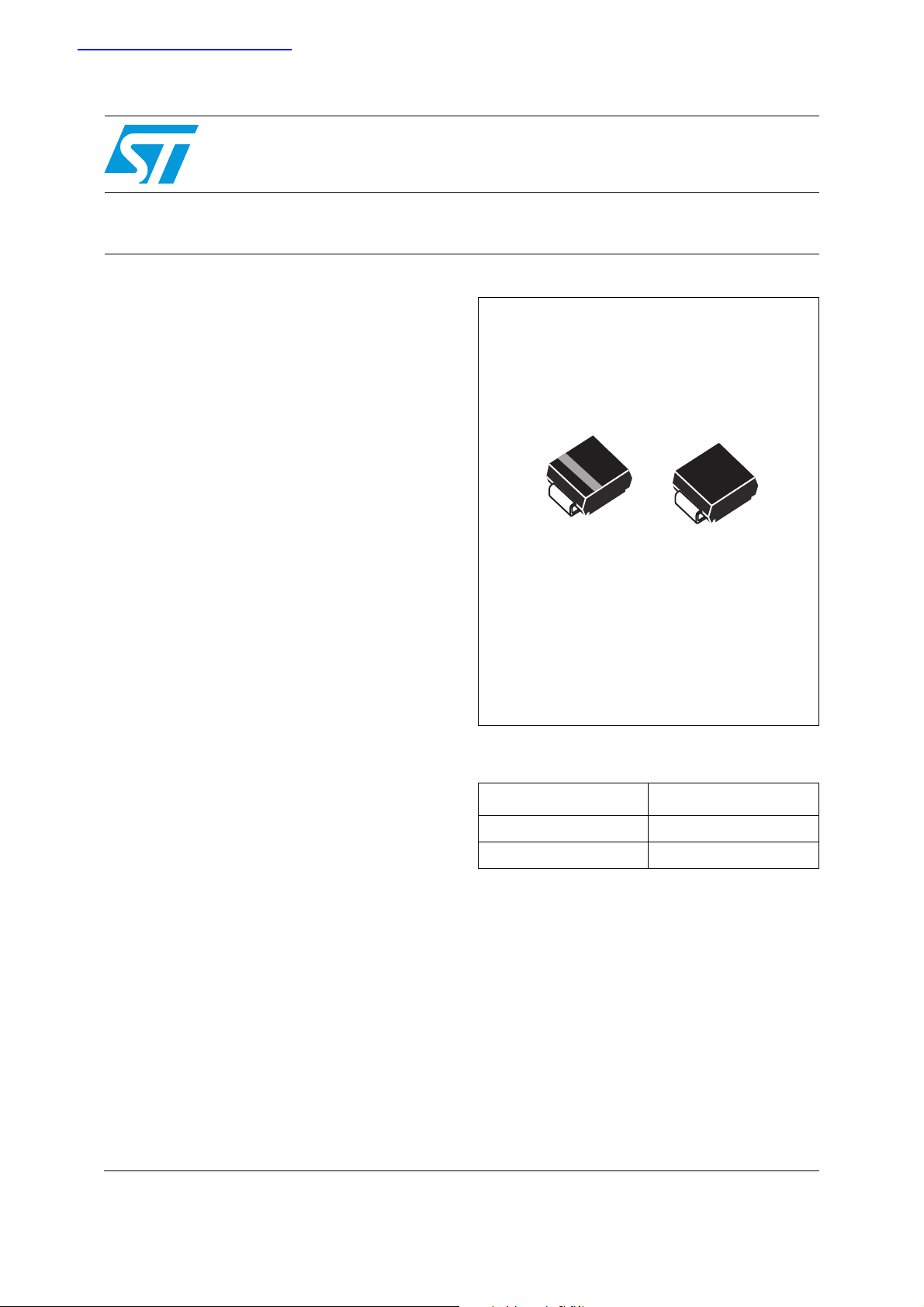
SMA6J
High junction temperature Transil™
A
K
Unidirectional Bidirectional
SMA
(JEDEC DO-214AC)
Description
The SMA6J Transil series has been designed to
protect sensitive equipment against electro-static
discharges according to IEC 61000-4-2, MIL STD
883 Method 3015, and electrical over stress such
as IEC 61000-4-4 & 5. They are also in
accordance with ISO TR 7637-2, SAE J 113 and
DIN 40839 for automotive applications and more
generally for surges below 600 W 10/1000 µs
This Planar technology makes it compatible with
high-end equipment like automotive, medical
equipment or SMPS where low leakage current
and high junction temperature are required to
provide reliability and stability over time. Their low
clamping voltages provides a better safety margin
to protect sensitive circuits with extended life time
expectancy.
Packaged in SMA, this minimizes PCB
consumption (SMA footprint in accordance with
IPC 7531 standard).
Order code
Part number Marking
SMA6JxxA-TR See Ta b l e 6 .
SMA6JxxCA-TR See Ta b l e 6 .
Complies with the following standards:
IEC 61000-4-2 level 4:
15 kV(air discharge)
8 kV(contact discharge)
MIL STD 893G-Method 3015-7: class3B
25 kV HBM (Human Body Model)
TM: TRANSIL is a trademark of STMicroelectronics
February 2007 Rev 1 1/10
www.st.com
10
Page 2
Characteristics SMA6J
1 Characteristics
Table 1. Absolute ratings (T
= 25° C)
amb
Symbol Parameter Value Unit
P
Peak pulse power dissipation
PP
P Power dissipation on infinite heatsink T
I
FSM
T
T
T
1. For a surge greater than the maximum values, the diode will fail in short-circuit.
Table 2. Thermal resistances
Non repetitive surge peak forward current for
unidirectional types
Storage temperature range -65 to +175 ° C
stg
Operating junction temperature range -55 to +175 ° C
j
Maximum lead temperature for soldering during 10 s 260 ° C
L
(1)
Tj initial = T
amb
amb
= 55° C 4 W
tp = 10 ms
Tj initial = T
amb
600 W
60 A
Symbol Parameter Value Unit
R
th (j-l)
R
th (j-a)
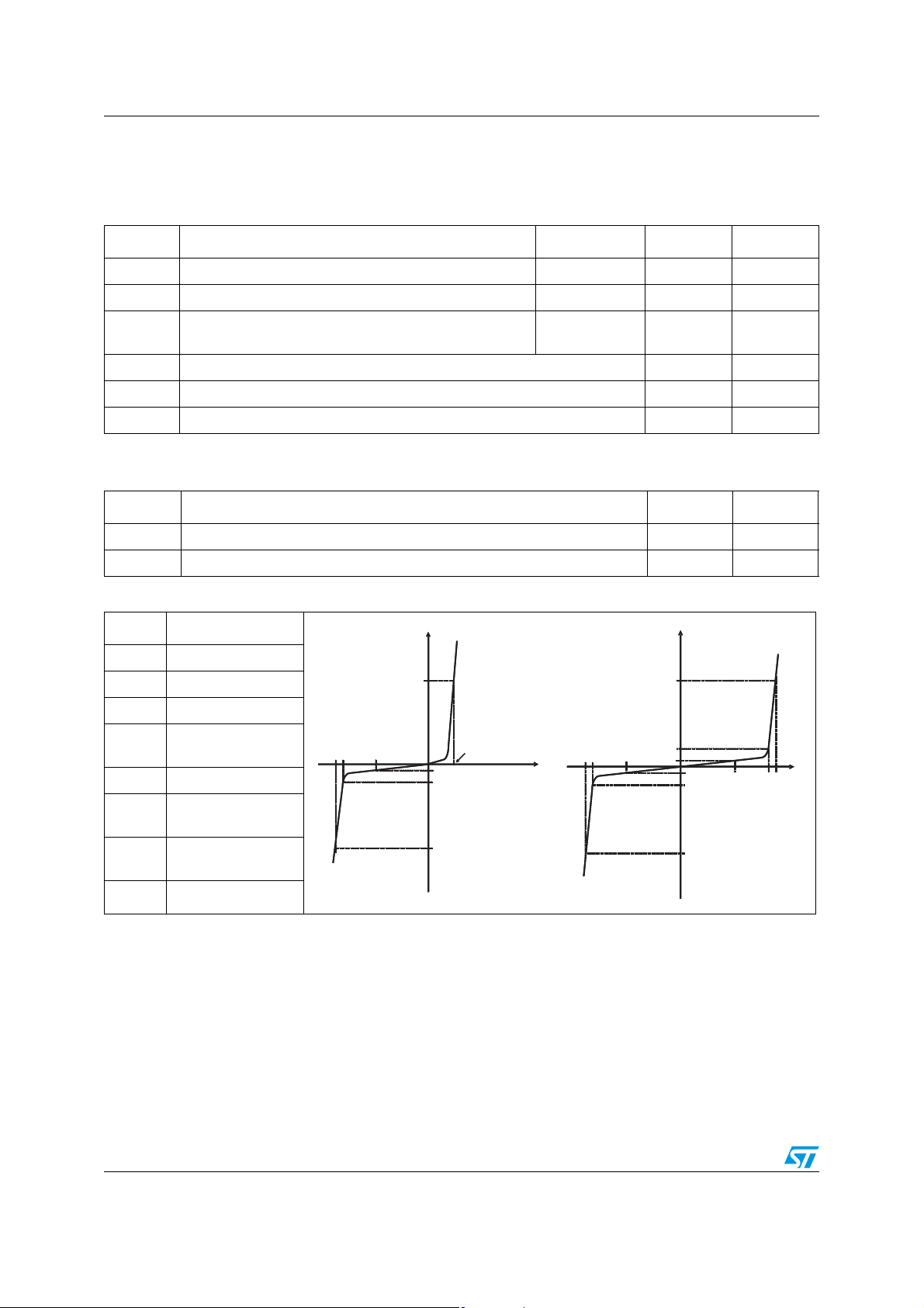
Table 3. Electrical characteristics - definitions (T
Symbol Parameter
V
RM
V
BR
V
CL
I
RM
I
PP
αT
V
F
Junction to leads 30 ° C/W
Junction to ambient on printed circuit on recommended pad layout 120 ° C/W
I
I
amb
= 25° C)
I
I
Stand-off voltage
I
Breakdown voltage
I
I
F
F
I
PP
PP
Clamping voltage
Leakage current
@ V
RM
Peak pulse current
Voltage temperature
VCLVBRV
VCLVBRV
RM
RM
V
V
F
F
I
I
RM
RM
I
I
R
R
V
V
VCLVBRV
VCLVBRV
RM
RM
I
I
R
R
I
I
RM
RM
I
I
VRMVBRV
VRMVBRV
RM
RM
I
I
R
R
coefficient
Unidirectional Bidirectional
I
Forward voltage
drop
I
PP
PP
I
I
PP
PP
V
V
CL
CL
R
Dynamic resistance
D
2/10
Page 3
SMA6J Characteristics
Type
max@VRM V
I
RM
BR
@I
R
(1)
amb
= 25° C)
VCL @IPP
10/1000 µs
(2)
R
D
10/1000 µs
VCL @IPP
8/20 µs
R
8/20 µs
25° C 85° C min typ max max max max
(2)
D
αT
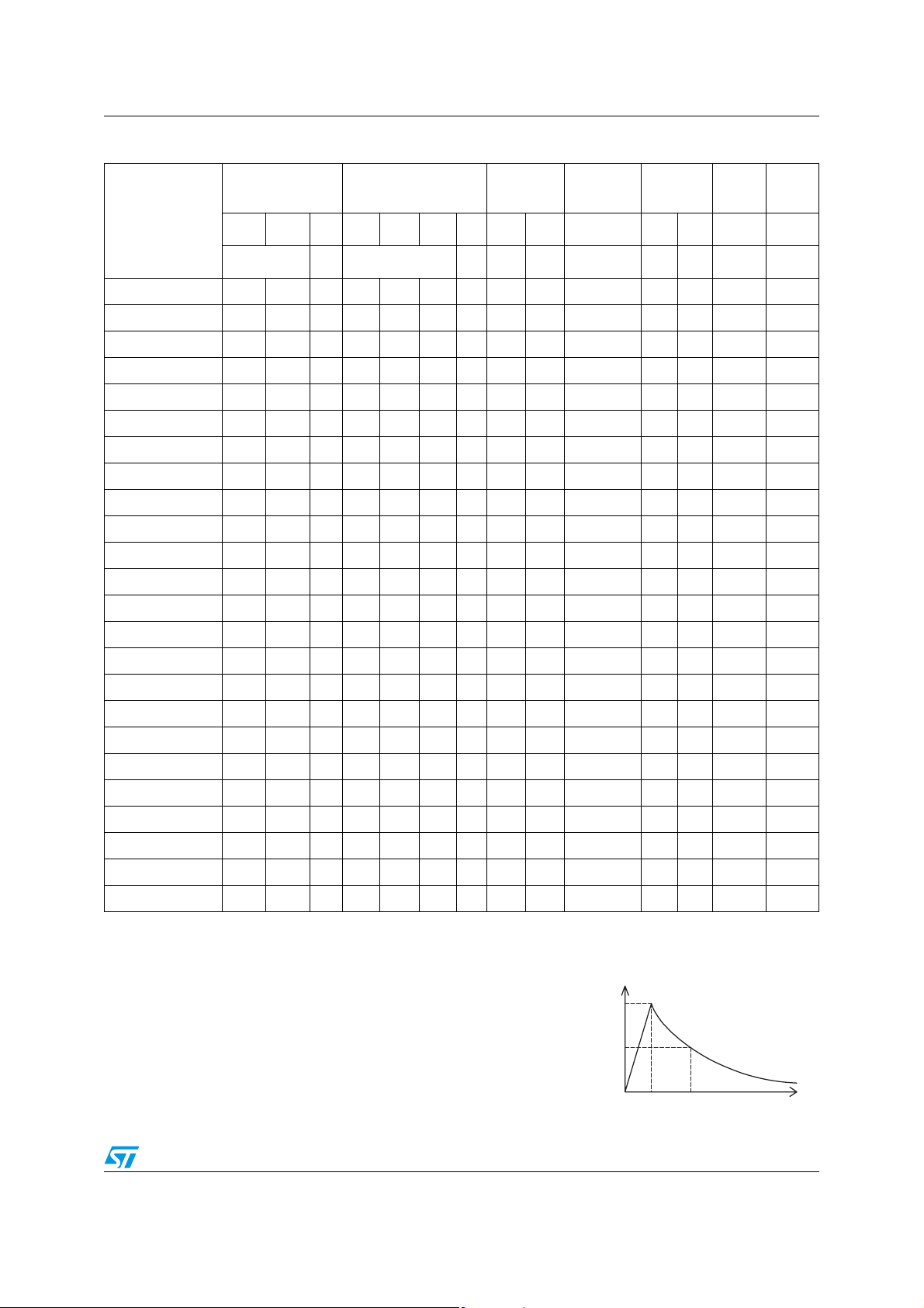
Table 4. Electrical characteristics - values (T
µA V V mA V A Ω VA Ω 10-4/°C
SMA6J5.0A/CA 10 50 5.0 6.40 6.74 7.07 10 9.1 68 0.029 13.4 298 0.021 5.7
SMA6J6.0A/CA 10 50 6.0 6.70 7.05 7.41 10 9.5 61 0.034 13.7 290 0.022 5.9
SMA6J6.5A/CA 10 50 6.5 7.20 7.58 7.96 10 10.2 56 0.040 14.5 276 0.024 6.1
SMA6J8.5A/CA 10 50 8.5 9.4 9.9 10.4 1 13.3 41.7 0.070 18.7 205 0.041 7.3
SMA6J10A/CA 0.2 1 10 11.1 11.7 12.3 1 15.7 37 0.093 19.6 184 0.040 7.8
SMA6J12A/CA 0.2 1 12 13.3 14.0 14.7 1 18.8 31 0.133 23.5 157 0.056 8.3
SMA6J13A/CA 0.2 1 13 14.4 15.2 15.9 1 20.4 29 0.154 23.9 147 0.054 8.4
SMA6J15A/CA 0.2 1 15 16.7 17.6 18.5 1 23.6 25.1 0.206 27.7 123 0.075 8.8
SMA6J18A/CA 0.2 1 18 20.0 21.1 22.1 1 28.3 21.5 0.288 33.2 102 0.108 9.2
SMA6J20A/CA 0.2 1 20 22.2 23.4 24.5 1 31.4 19.4 0.354 36.8 93 0.132 9.4
SMA6J24A/CA 0.2 1 24 26.7 28.1 29.5 1 37.8 16 0.516 44.3 80 0.184 9.6
SMA6J26A/CA 0.2 1 26 28.9 30.4 31.9 1 40.9 14.9 0.600 47.9 75 0.213 9.7
SMA6J28A/CA 0.2 1 28 31.1 32.7 34.4 1 44.0 13.8 0.697 51.6 68 0.253 9.8
(3)
SMA6J33A/CA 0.2 1 33 36.7 38.6 40.6 1 51.9 11.8 0.963 60.8 57 0.356 10.0
SMA6J40A/CA 0.2 1 40 44.4 46.7 49.1 1 62.8 9.7 1.42 73.6 48 0.511 10.1
SMA6J48A/CA 0.2 1 48 53.3 56.1 58.9 1 75.4 8.1 2.04 88.4 40 0.736 10.3
SMA6J58A/CA 0.2 1 58 64.4 67.8 71.2 1 91.1 6.7 2.97 100 33 0.863 10.4
SMA6J70A/CA 0.2 1 70 77.8 81.9 86.0 1 110 5.5 4.38 120 27 1.27 10.5
SMA6J85A/CA 0.2 1 85 94 99 104 1 134 4.6 6.45 146 22.5 1.85 10.6
SMA6J100A/CA 0.2 1 100 111 117 123 1 157 3.8 9.03 172 19 2.58 10.7
SMA6J130A/CA 0.2 1 130 144 152 159 1 204 3 14.9 223 15 4.24 10.8
SMA6J154A/CA 0.2 1 154 171 180 189 1 242 2.4 22.1 265 12.6 6.00 10.8
SMA6J170A/CA 0.2 1 170 189 199 209 1 275 2.2 30.0 292 11.3 7.39 10.8
SMA6J188A/CA 0.2 1 188 209 220 231 1 328 2 48.5 323 10.3 8.97 10.8
1. Pulse test: tp <50ms.
2. To calculate maximum clamping voltage at other surge currents, use the following formula
V
= RD x IPP + V
CLmax
3. To calculate VBR versus junction temperature, use the following formula:
VBR @ Tj = VBR @ 25 ° C x (1 + αT x (Tj - 25))
BRmax
100
50
%I
PP
Repetitive peak pulse current
tr = rise time (µs)
tp = pulse duration time (µs)
0
t
t
r
p
t
3/10
Page 4
Characteristics SMA6J
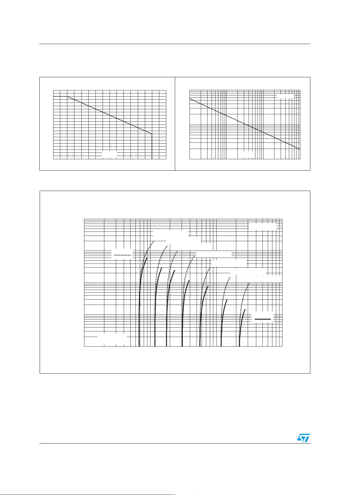
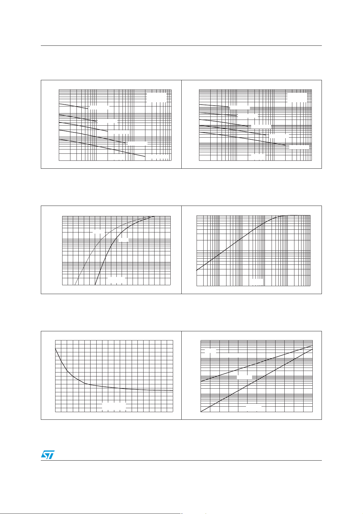
Figure 1. Peak power dissipation versus
Figure 2. Peak pulse power versus
initial junction temperature
%
110
100
90
80
70
60
50
40
30
20
10
0
0 25 50 75 100 125 150 175 200
T (°C)
j
P (kW)
10.0
1.0
0.1
0.01 0.10 1.00 10.00
Figure 3. Clamping voltage versus peak pulse current
(exponential waveform, maximum values)
I (A)
PP
1.E+03
SMA6J5.0A/CA
SMA6J10A/CA
1.E+02
t = 20 µs
p
SMA6J15A/CA
1.E+01
exponential pulse duration
(T
initial = 25° C)
j
PP
t (ms)
p
SMA6J26A/CA
SMA6J48A/CA
SMA6J100A/CA
T = 25°C
j
SMA6J188A/CA
T initial=25°C
j
1.E+00
V (V)
CL
1.E-01
1 10 100 1000
4/10
t = 1 ms
p
Page 5
SMA6J Characteristics
Figure 4. Junction capacitance versus
reverse applied voltage (typical
values) (SMA6JxxA)
C(pF)
10000
1000
100
10
1 10 100 1000
SMA6J5.0A
SMA6J13A
SMA6J26A
SMA6J58A
V (V)
R
F=1MHz
V =30mV
OSC RMS
T =25°C
j
SMA6J188A
Figure 6. Peak forward voltage drop versus
peak forward current (typical
values)
I (A)
FM
1.E+01
T =125°C
j
1.E+00
T =25°C
j
Figure 5. Junction capacitance versus
reverse applied voltage (typical
values) (SMA6JxxCA)
C(pF)
10000
1000
100
10
1
1 10 100 1000
SMA6J5.0CA
SMA6J13CA
SMA6J26CA
V (V)
R
SMA6J58CA
F=1MHz
V =30mV
OSC RMS
T =25°C
j
SMA6J188CA
Figure 7. Relative variation of thermal
impedance junction to ambient
versus pulse duration (printed
1.00
Z
ciruit board FR4, S
th(j-a)/Rth(j-a)
= 1 cm2)
Cu
1.E-01
V (V)
1.E-02
0.4 0.5 0.6 0.7 0.8 0.9 1.0 1.1 1.2 1.3 1.4
FM
Figure 8. Thermal resistance junction to
ambient versus copper surface
under each lead (printed circuit
board FR4, e
R
(°C/W)
th(j-a)
130
120
110
100
90
80
70
60
50
40
0.0 0.5 1.0 1.5 2.0 2.5 3.0 3.5 4.0 4.5 5.0
Cu
S (cm )
CU
= 35 µm)
2
0.10
t (S)
0.01
1.E-02 1.E-01 1.E+00 1.E+01 1.E+02 1.E+03
p
Figure 9. Leakage current versus junction
temperature (typical values)
I (nA)
R
1.E+04
V=RV
RM
1.E+03
1.E+02
1.E+01
1.E+00
25 50 75 100 125 150 175
V 11.7VBR≤
>
V 11.7V
BR
T (°C)
j
5/10
Page 6
Order information scheme SMA6J
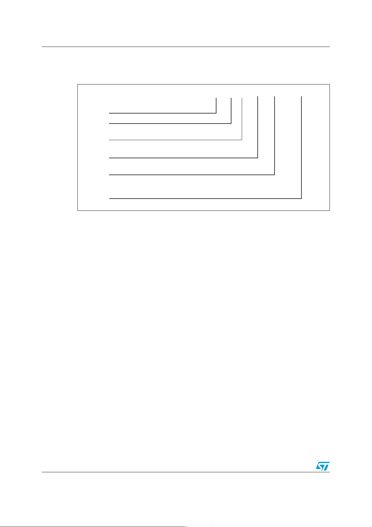
2 Order information scheme
SM A 6J xx CA - TR
Surface Mount
Package
A = SMA package
Surge rating
6J = 600 W
Stand off voltage
example - 85 = 85 V
Type
A = Unidirectional
CA = Bidirectional
Packaging
TR = Tape and reel
6/10
Page 7
SMA6J Package information
3 Package information
● Case: JEDEC DO-214AC molded plastic over Planar junction
● Terminals: Solder plated, solderable per MIL-STD-750, Method 2026
● Polarity: For unidirectional types the band indicates cathode.
● Flammability: Epoxy is rated UL94V-0
● RoHS package
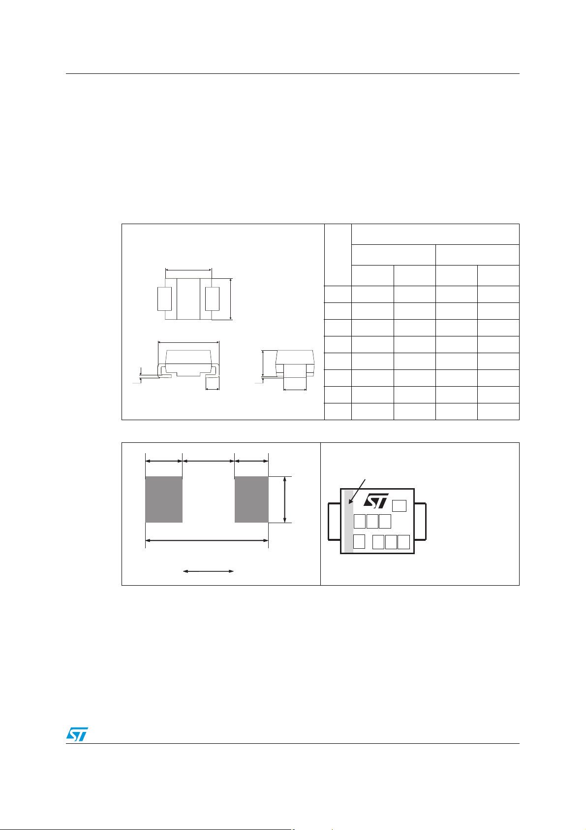
Table 5. SMA Dimensions
Dimensions
Ref.
E1
Millimeters Inches
Min. Max. Min. Max.
D
A1 1.90 2.03 0.075 0.08
A2 0.05 0.20 0.002 0.008
b 1.25 1.65 0.049 0.065
E
A1
C
L
A2
b
c 0.15 0.40 0.006 0.016
D 2.25 2.90 0.089 0.114
E 4.80 5.35 0.189 0.211
E1 3.95 4.60 0.156 0.181
L 0.75 1.50 0.030 0.059
Figure 10. SMA footprint dimensions Figure 11. Marking information
1.40
1.40
(0.055)
(0.055)
2.63
2.63
(0.104)
(0.104)
5.43
5.43
(0.214)
(0.214)
1.40
1.40
(0.055)
(0.055)
1.64
1.64
Cathode bar (
(0.065)
(0.065)
unidirectional
e3
x x x
y w w
z
devices only )
e3: ECOPACK (Leadfree)
XXX: Marking
Z: Manufacturing location
Y: Year
WW: week
milimeters
milimeters
(inches)
(inches)
7/10
Page 8
Package information SMA6J
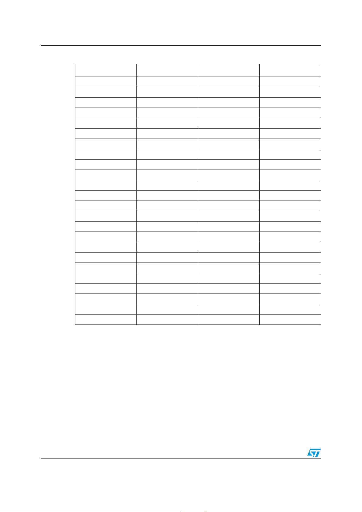
Table 6. Marking
Type Marking Type Marking
SMA6J5.0A-TR 6UA SMA6J5.0CA-TR 6BA
SMA6J6.0A-TR 6UB SMA6J6.0CA-TR 6BB
SMA6J6.5A-TR 6UC SMA6J6.5CA-TR 6BC
SMA6J8.5A-TR 6UD SMA6J8.5CA-TR 6BD
SMA6J10A-TR 6UE SMA6J10CA-TR 6BE
SMA6J12A-TR 6UF SMA6J12CA-TR 6BF
SMA6J13A-TR 6UG SMA6J13CA-TR 6BG
SMA6J15A-TR 6UH SMA6J15CA-TR 6BH
SMA6J18A-TR 6UJ SMA6J18CA-TR 6BJ
SMA6J20A-TR 6UK SMA6J20CA-TR 6BK
SMA6J24A-TR 6UM SMA6J24CA-TR 6BM
SMA6J26A-TR 6UN SMA6J26CA-TR 6BN
SMA6J28A-TR 6UO SMA6J28CA-TR 6BO
SMA6J33A-TR 6UQ SMA6J33CA-TR 6BQ
SMA6J40A-TR 6UR SMA6J40CA-TR 6BR
SMA6J48A-TR 6US SMA6J48CA-TR 6BS
SMA6J58A-TR 6UT SMA6J58CA-TR 6BT
SMA6J70A-TR 6UU SMA6J70CA-TR 6BU
SMA6J85A-TR 6UV SMA6J85CA-TR 6BV
SMA6J100A-TR 6UW SMA6J100CA-TR 6BW
SMA6J130A-TR 6UX SMA6J130CA-TR 6BX
SMA6J154A-TR 6UY SMA6J154CA-TR 6BY
SMA6J170A-TR 6UZ SMA6J170CA-TR 6BZ
SMA6J188A-TR 6UAA SMA6J188CA-TR 6BAA
In order to meet environmental requirements, ST offers these devices in ECOPACK®
packages. These packages have a Lead-free second level interconnect . The category of
second level interconnect is marked on the package and on the inner box label, in
compliance with JEDEC Standard JESD97. The maximum ratings related to soldering
conditions are also marked on the inner box label. ECOPACK is an ST trademark.
ECOPACK specifications are available at: www.st.com.
8/10
Page 9
SMA6J Ordering information
4 Ordering information
Part number Marking Package Weight Base qty
SMA6JxxA-TR See Table 6. SMA 0.068 g 5000 Tape and reel
SMA6JxxCA-TR See Table 6. SMA 0.068 g 5000 Tape and reel
Delivery
mode
5 Revision history
Date Revision Changes
21-Feb-2007 1 First issue.
9/10
Page 10

SMA6J
Please Read Carefully:
Information in this document is provided solely in connection with ST products. STMicroelectronics NV and its subsidiaries (“ST”) reserve the
right to make changes, corrections, modifications or improvements, to this document, and the products and services described herein at any
time, without notice.
All ST products are sold pursuant to ST’s terms and conditions of sale.
Purchasers are solely responsible for the choice, selection and use of the ST products and services described herein, and ST assumes no
liability whatsoever relating to the choice, selection or use of the ST products and services described herein.
No license, express or implied, by estoppel or otherwise, to any intellectual property rights is granted under this document. If any part of this
document refers to any third party products or services it shall not be deemed a license grant by ST for the use of such third party products
or services, or any intellectual property contained therein or considered as a warranty covering the use in any manner whatsoever of such
third party products or services or any intellectual property contained therein.
UNLESS OTHERWISE SET FORTH IN ST’S TERMS AND CONDITIONS OF SALE ST DISCLAIMS ANY EXPRESS OR IMPLIED
WARRANTY WITH RESPECT TO THE USE AND/OR SALE OF ST PRODUCTS INCLUDING WITHOUT LIMITATION IMPLIED
WARRANTIES OF MERCHANTABILITY, FITNESS FOR A PARTICULAR PURPOSE (AND THEIR EQUIVALENTS UNDER THE LAWS
OF ANY JURISDICTION), OR INFRINGEMENT OF ANY PATENT, COPYRIGHT OR OTHER INTELLECTUAL PROPERTY RIGHT.
UNLESS EXPRESSLY APPROVED IN WRITING BY AN AUTHORIZED ST REPRESENTATIVE, ST PRODUCTS ARE NOT
RECOMMENDED, AUTHORIZED OR WARRANTED FOR USE IN MILITARY, AIR CRAFT, SPACE, LIFE SAVING, OR LIFE SUSTAINING
APPLICATIONS, NOR IN PRODUCTS OR SYSTEMS WHERE FAILURE OR MALFUNCTION MAY RESULT IN PERSONAL INJURY,
DEATH, OR SEVERE PROPERTY OR ENVIRONMENTAL DAMAGE. ST PRODUCTS WHICH ARE NOT SPECIFIED AS "AUTOMOTIVE
GRADE" MAY ONLY BE USED IN AUTOMOTIVE APPLICATIONS AT USER’S OWN RISK.
Resale of ST products with provisions different from the statements and/or technical features set forth in this document shall immediately void
any warranty granted by ST for the ST product or service described herein and shall not create or extend in any manner whatsoever, any
liability of ST.
ST and the ST logo are trademarks or registered trademarks of ST in various countries.
Information in this document supersedes and replaces all information previously supplied.
The ST logo is a registered trademark of STMicroelectronics. All other names are the property of their respective owners.
© 2007 STMicroelectronics - All rights reserved
STMicroelectronics group of companies
Australia - Belgium - Brazil - Canada - China - Czech Republic - Finland - France - Germany - Hong Kong - India - Israel - Italy - Japan -
Malaysia - Malta - Morocco - Singapore - Spain - Sweden - Switzerland - United Kingdom - United States of America
www.st.com
10/10
 Loading...