

STMicroelectronics PD55008S-E Service Manual

www.DataSheet4U.com
N-Channel enhancement-mode lateral MOSFETs
General features
■ Excellent thermal stability
■ Common source configuration
■ P
■ New RF plastic package
Description
= 8W with 17dB gain @ 500MHz / 12.5V
OUT
PD55008-E
PD55008S-E
RF POWER transistor, LDMOST plastic family
PowerSO-10RF
(formed lead)
The PD55008 is a common source N-Channel,
enhancement-mode lateral Field-Effect RF power
transistor. It is designed for high gain, broad band
commercial and industrial applications. It
operates at 12 V in common source mode at
frequencies up to 1 GHz.
PD55008 boasts the excellent gain, linearity and
reliability of ST’s latest LDMOS technology
mounted in the first true SMD plastic RF power
package, PowerSO-10RF. PD55008’s superior
linearity performance makes it an ideal solution
for car mobile radio.
The PowerSO-10 plastic package, designed to
offer high r elia bility, is the first ST JEDE C
approved, high power SMD package. It has been
specially optimized for RF needs and offers
excellent RF performances and ease of
assembly.
Mounting recommendations are available in
www.st.com/rf/ (look for application note AN1294)
PowerSO-10RF
(straight lead)
Pin conn ection
Gate
Source
Drain
Order codes
Part number Package Packing
PD55008-E PowerSO-10RF (formed lead) Tube
PD55008S-E PowerSO-10RF (straight lead) Tube
PD55008TR-E PowerSO-10RF (formed lead) Tape and reel
PD55008STR-E PowerSO-10RF (straight lead) Tape and reel
April 200 6 Rev 1 1/28
www.st.com
28

Contents PD55008-E, PD55008S-E
Contents
1 Electrical data . . . . . . . . . . . . . . . . . . . . . . . . . . . . . . . . . . . . . . . . . . . . . . 3
1.1 Maximum ratings . . . . . . . . . . . . . . . . . . . . . . . . . . . . . . . . . . . . . . . . . . . . 3
1.2 Thermal data . . . . . . . . . . . . . . . . . . . . . . . . . . . . . . . . . . . . . . . . . . . . . . . 3
2 Electrical Characteristics . . . . . . . . . . . . . . . . . . . . . . . . . . . . . . . . . . . . . 4
2.1 Static . . . . . . . . . . . . . . . . . . . . . . . . . . . . . . . . . . . . . . . . . . . . . . . . . . . . . . 4
2.2 Dynamic . . . . . . . . . . . . . . . . . . . . . . . . . . . . . . . . . . . . . . . . . . . . . . . . . . . 4
3 Impedance . . . . . . . . . . . . . . . . . . . . . . . . . . . . . . . . . . . . . . . . . . . . . . . . . 5
4 Typical performance . . . . . . . . . . . . . . . . . . . . . . . . . . . . . . . . . . . . . . . . . 6
5 Test circuit . . . . . . . . . . . . . . . . . . . . . . . . . . . . . . . . . . . . . . . . . . . . . . . . 13
6 Circuit layout . . . . . . . . . . . . . . . . . . . . . . . . . . . . . . . . . . . . . . . . . . . . . . 15
7 Common source s-parameter . . . . . . . . . . . . . . . . . . . . . . . . . . . . . . . . 16
7.1 PD55008 (VDS = 12.5V IDS = 150mA) . . . . . . . . . . . . . . . . . . . . . . . . . . 16
7.2 PD55008 (VDS = 12.5V IDS = 800mA) . . . . . . . . . . . . . . . . . . . . . . . . . . 17
7.3 PD55008 (VDS = 12.5V IDS = 1.5A) . . . . . . . . . . . . . . . . . . . . . . . . . . . . 18
7.4 PD55008S (VDS = 12.5V IDS = 150mA) . . . . . . . . . . . . . . . . . . . . . . . . . 19
7.5 PD55008S (VDS = 12.5V IDS = 800mA) . . . . . . . . . . . . . . . . . . . . . . . . . 20
7.6 PD55008S (VDS = 12.5V IDS = 1.5A) . . . . . . . . . . . . . . . . . . . . . . . . . . . 21
8 Mechanical data . . . . . . . . . . . . . . . . . . . . . . . . . . . . . . . . . . . . . . . . . . . . 22
9 Revision history . . . . . . . . . . . . . . . . . . . . . . . . . . . . . . . . . . . . . . . . . . . 27
2/28
PD55008-E, PD55008S-E Electrical data
1 Electrical data
1.1 Maximum ratings
Table 1. Absolute maximum ratings (T
Symbol Parameter Value Unit
V
(BR)DSS
V
GS
I
D
P
DISS
T
J
T
STG
1.2 Thermal data
Table 2. Thermal data
Symbol Parameter Value Unit
R
thJC
= 25°C)
CASE
Drain-source voltage 40 V
Gate-source voltage ± 20 V
Drain current 4 A
Power dissipati on (@ TC = 70°C) 52.8 W
Max. operating junction temperature 165 °C
St orage temperature -65 to +150 °C
Junction - case thermal resistance 1.8 °C/W
3/28
Electrical Characteristics PD55008-E, PD55008S-E
2 Electrical Characteristics
T
= +25 oC
CASE
2.1 Static
Table 3. Static
Symbol Test conditions Min. Typ. Max. Unit
I
DSS
I
GSS
V
GS(Q)
V
DS(ON)VGS
g
FS
C
ISS
C
OSS
C
RSS
2.2 Dynamic
Table 4. Dynamic
Symbol Test conditions Min. Typ. Max. Unit
P
OUT
G
P
n
D
Load
mismatch
VGS = 0V VDS = 28V 1 µA
VGS = 20V VDS = 0V 1 µA
VDS = 10V
= 150mA 2.0 5.0 V
ID
= 10V ID = 1.5A 0.67 V
VDS = 10V ID = 1.5A 1.6 mho
VGS = 0V VDS = 12.5V f = 1MHz 58 pF
VGS = 0V VDS = 12.5V f = 1MHz 38 pF
VGS = 0V VDS = 12.5V f = 1MHz 2.8 pF
VDD = 12.5V, IDQ = 150mA f = 500MHz 8 W
VDD = 12.5V, IDQ = 150mA, P
VDD = 12.5V, IDQ = 150mA, P
V
= 15.5V, IDQ = 150mA, P
DD
All phase angles
= 8W, f = 500MHz 15 17 dB
OUT
= 8W, f = 500MHz 50 55 %
OUT
= 8W, f = 500MHz
OUT
20:1 VSWR
4/28
PD55008-E, PD55008S-E Impedance
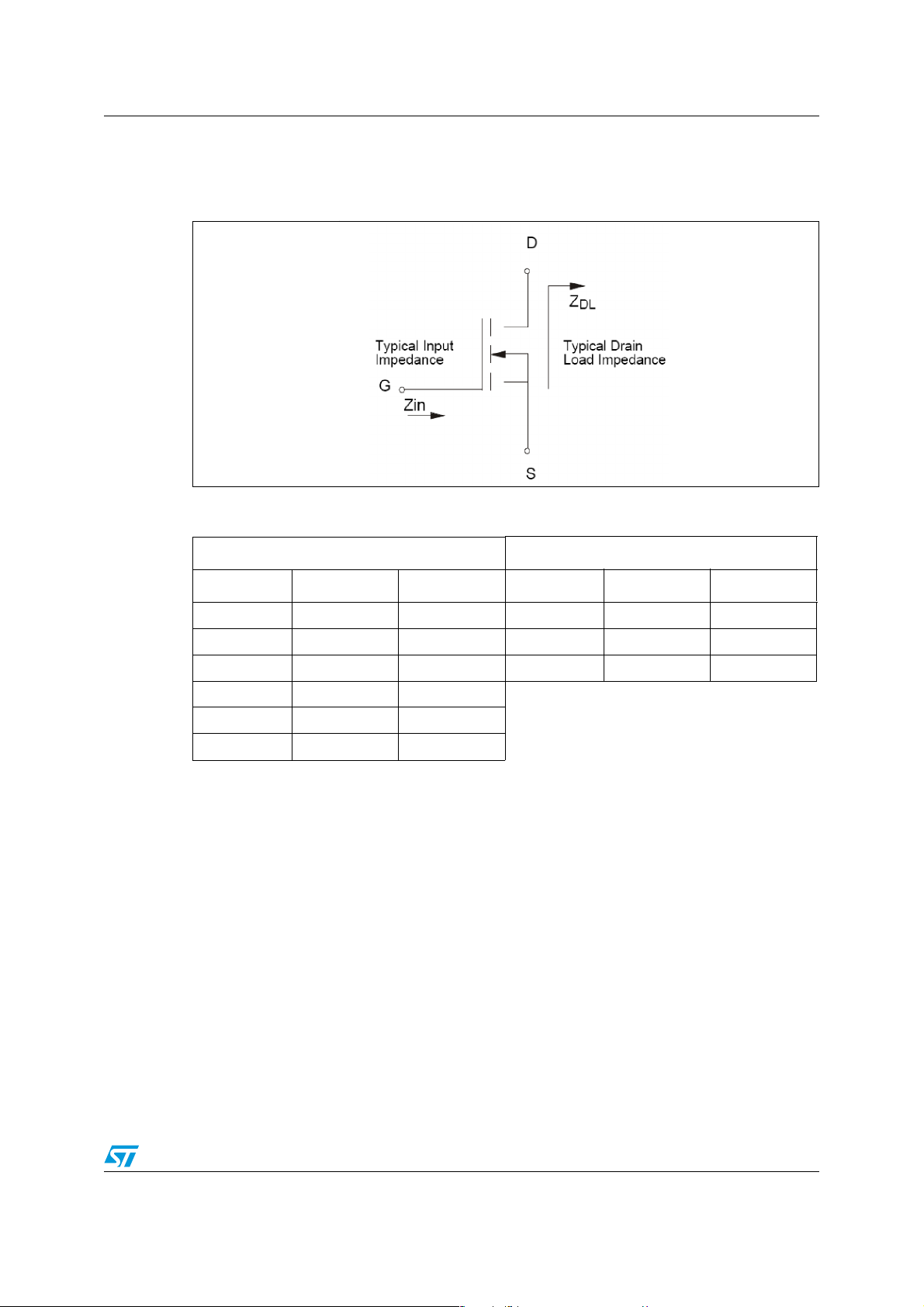
3 Impedance
Figure 1. Current conventions
Table 5. Impedance data
PD55008 PD55008S
Freq. (MHz) ZIN (Ω) ZDL(Ω)Freq. (MHz)Z
480 1.141 - j 2.054 1.649 + j 2.916 480 1.075 - j 2.727 2.046 + j 1.960
500 1.589 - j 1.185 1.561 + j 2.639 500 1.409 - j 3.448 2.129 + j 3.219
520 1.649 - j 1.965 1.716 + j 1.552 520 1.586 - j 2.087 3.082 + j 2.043
800 1.05 + j 0.54 2.62 - j 1.91
850 1.50 + j 1.00 2.26 - j 1.54
900 1.95 + j 2.28 2.70 - j 1.90
(Ω)Z
IN
DL
(Ω)
5/28
Typical performance PD55008-E, PD55008S-E
5
6
0
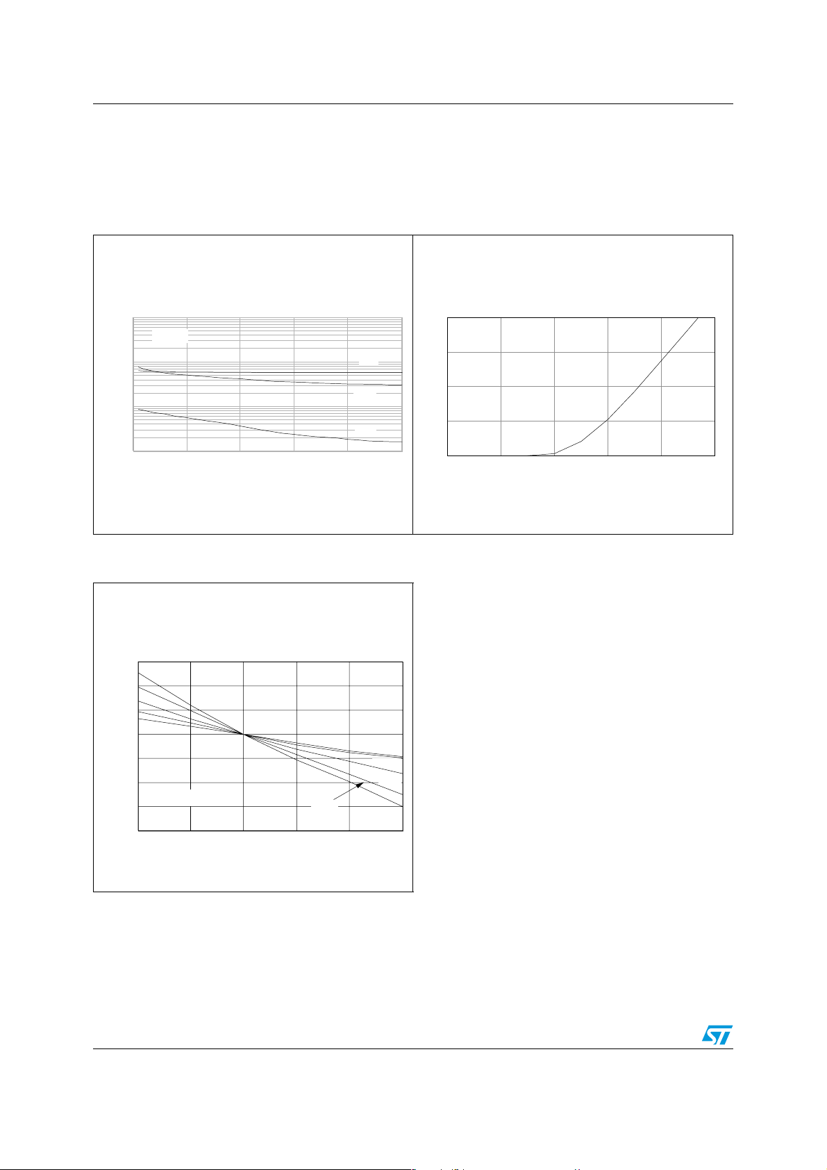
4 Typical performance
Figure 2. Capacitance vs. drain voltage Figure 3. Drain current vs. gate-source
voltage
1000
f=1 MHz
100
10
Coss
C, CAPACITANCES (pF)
1
0 5 10 15 20 2
Crss
VDD, DRAIN VOLT AGE (V)
Figure 4. Gate-source voltage vs. case
temperature
1.06
1.04
1.02
Ciss
4
3
2
1
Id, DRAIN CURRENT (A)
0
12345
VGS, G ATE-SOURCE VOLTAGE (V )
Vds = 10 V
1
0.98
0.96
0.94
VGS, GATE-SOURCE VOLTAGE(NORMALIZED)
0.92
VDS= 10 V
-25 0 25 50 75 10
Tc, CASE TEMPERATURE (°C)
ID= .5A
=
I
D
ID= 2A
ID= 1.5A
ID= 1A
.25A
6/28
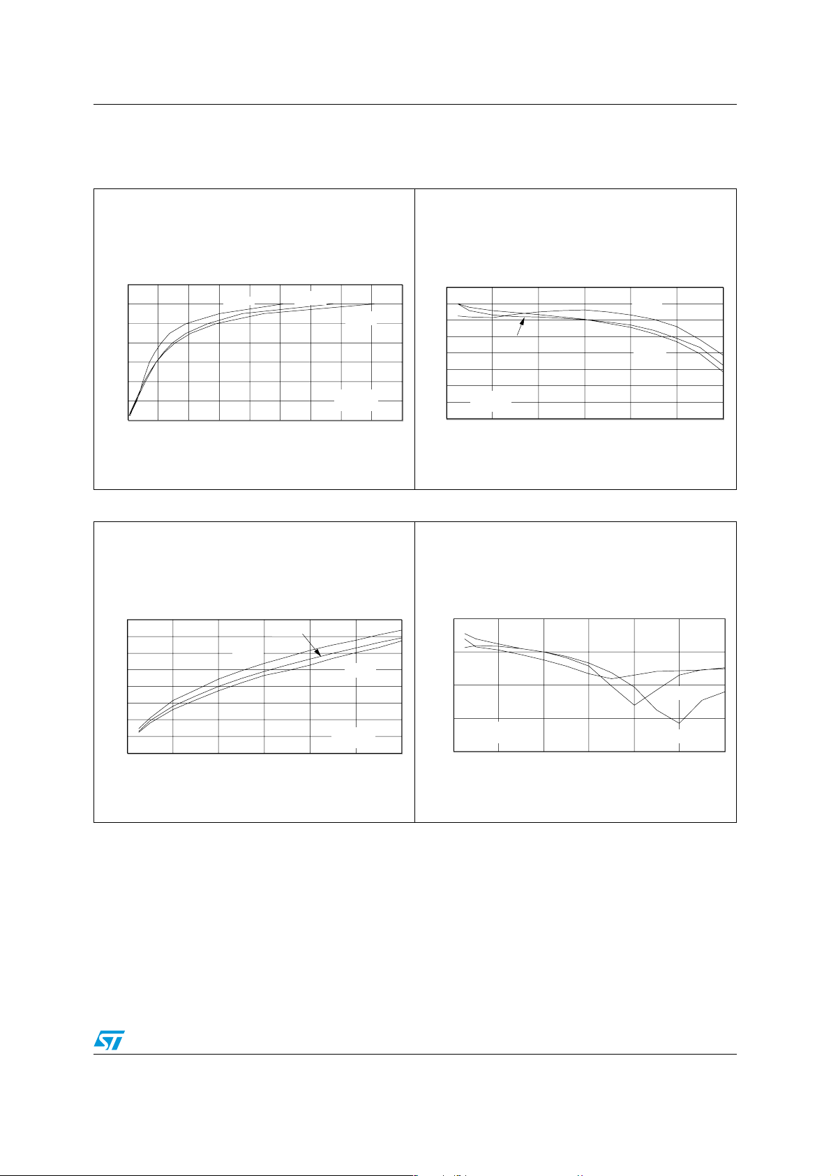
PD55008-E, PD55008S-E Typical performance
9
2
PD55008
Figure 5. Output power vs. input power Figure 6. Power gain vs. output power
14
12
480 MHz
10
520 MHz
500 MHz
8
6
4
2
Pout, OUTPUT P OWER (W)
0
0 0.1 0.2 0.3 0.4 0.5 0.6 0.7 0.8 0.
VDD= 12.5 V
= 150 mA
I
DQ
Pin, INPUT POWER (W)
Figure 7. Drain efficiency vs. output power Figure 8. Input return loss vs. output power
22
20
18
16
14
12
10
Pg, POWER GAIN (dB)
8
6
024681012
VDD= 12.5 V
I
= 150 mA
DQ
520 MHz
80
70
60
50
520 MHz
500 MHz
480 MHz
40
0
-10
-20
480 MHz
500 MHz
Pout, OUTPUT POWER (W )
500 MHz
480 MHz
30
20
10
Nd, DRAIN EFFICIE NCY (%)
0
024681012
VDD= 12.5 V
= 150 mA
I
DQ
Pout, OUTPUT POWER (W)
-30
VDD= 12.5 V
I
= 150 mA
DQ
Rtl, INPUT RETURN LOSS (dB )
-40
02468101
520 MH z
Pout, OUTPUT POWER (W)
7/28

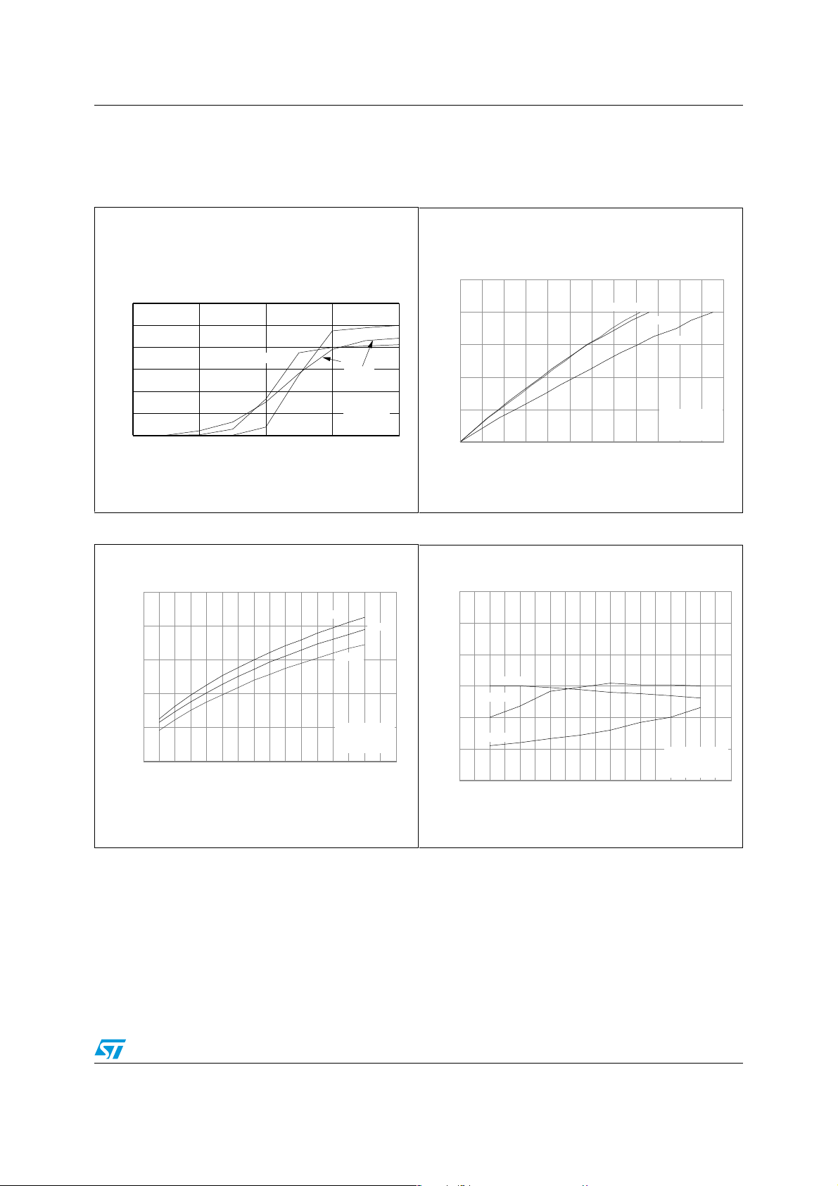
Typical performance PD55008-E, PD55008S-E
PD55008
Figure 9. Output power vs. bias current Figure 10. Drain efficiency vs. bias current
12
10
8
500 MHz
6
480 MHz
520 MHz
4
2
Pout, OUTPUT P O WER (W)
0
0 100 200 300 400 500 600 700 800
VDD= 12.5 V
Pin= 21.7 dBm
IDQ, BIAS CURRENT (mA)
Figure 11. Output power vs. supply voltage Figure 12. Drain efficiency vs. supply voltage
70
60
50
40
30
20
Nd, DRAIN EFFICIENCY (%)
10
0 100 200 300 400 500 600 700 800
480 MHz
13
12
11
10
9
8
7
6
5
Pout, OUTPUT POWER (W)
4
3
9 101112131415
500 MHz
VDD, SUPPLY VOLTAGE (V)
480 MHz
520 MHz
Idq= 150 mA
Pin= 21.7 dB m
70
60
50
40
30
Nd, DRAIN EFFICIENCY (%)
20
9 101112131415
VDD, SUPPLY VOLTAGE (V)
520 MHz
IDQ, BIAS CURRENT (mA)
480 MHz
500 MHz
VDD= 12.5 V
Pin= 21.7 dBm
500 MHz
520 MHz
Idq= 150 mA
Pin= 21.7 dBm
8/28
PD55008-E, PD55008S-E Typical performance
PD55008
Figure 13. Output power vs. gate-source
voltage
Table 6. Output power vs. input power
10
12
10
8
6
4
2
Pout, OUTPUT POWER (W)
0
01234
Figure 14. Drain efficiecy vs. output power Figure 15. Input return loss vs. output power
60
VGS, GATE-SOURCE VOLTAGE (V)
500 MHz
50
40
30
Drain efficiency (%)
20
10
123456789
Output Power (W)
850 MHz
800 MHz
480 MHz
520 MHz
VDD= 12.5 V
Pin= 21.7 dBm
900 MHz
Vdd = 12.5V
Idq = 250mA
8
6
4
Output Power (W)
2
0
0 0.1 0.2 0.3 0.4 0.5 0.6
0
-5
-10
-15
-20
Input Return Loss (dB)
800 MHz
900 MHz
850 MHz
-25
-30
0123456789
800 MHz
Input Power (W)
Output Power (W)
850 MHz
900 MHz
Vdd = 12.5V
Idq = 250mA
Vdd = 12.5V
Idq = 250mA
9/28
 Loading...