

Page 1

UM2592
User manual
STM32WL Nucleo-64 board (MB1389)
Introduction
The NUCLEO-WL55JC STM32WL Nucleo-64 board, based on the MB1389 reference board (NUCLEO-WL55JC1 and
NUCLEO-WL55JC2 order codes), provides an affordable and flexible way for users to try out new concepts and build prototypes
with the STM32WL Series microcontroller, choosing from the various combinations of performance, power consumption, and
features.
The ARDUINO® Uno V3 connectivity support and the ST morpho headers provide an easy means of expanding the functionality
of the STM32WL Nucleo open development platform with a wide choice of specialized shields.
The STM32WL Nucleo-64 board does not require any separate probe as it integrates the STLINK-V3E debugger and
programmer.
The STM32WL Nucleo-64 board is provided with the STM32WL comprehensive software HAL library and various packaged
software examples available with the STM32CubeWL MCU Package.
Figure 1. NUCLEO-WL55JC top view
Pictures are not contractual.
Figure 2. NUCLEO-WL55JC bottom view
UM2592 - Rev 1 - November 2020
For further information contact your local STMicroelectronics sales office.
www.st.com
Page 2

1 Features
• STM32WL55JC microcontroller multiprotocol LPWAN dual-core 32-bit (Arm® Cortex®-M4/M0+ at 48 MHz) in
UFBGA73 package featuring:
– Ultra-low-power MCU
– RF transceiver (150 MHz to 960 MHz frequency range) supporting LoRa®, (G)FSK, (G)MSK, and
BPSK modulations
– 256-Kbyte Flash memory and 64-Kbyte SRAM
• 3 user LEDs
• 3 user buttons and 1 reset push-button
• 32.768 kHz LSE crystal oscillator
• 32 MHz HSE on-board oscillator
• Board connectors:
– USB with Micro-B
–
MIPI® debug connector
–
ARDUINO® Uno V3 expansion connector
– ST morpho extension pin headers for full access to all STM32WL I/Os
• Delivered with SMA antenna
• Flexible power-supply options: ST-LINK, USB V
• On-board STLINK-V3 debugger/programmer with USB re-enumeration capability: mass storage, Virtual
COM port, and debug port
• Comprehensive free software libraries and examples available with the STM32CubeWL MCU Package
• Support of a wide choice of Integrated Development Environments (IDEs) including IAR Embedded
Workbench®, MDK-ARM, and STM32CubeIDE
• Suitable for rapid prototyping of end nodes based on LoRaWAN®, Sigfox™, wM-Bus, and many other
proprietary protocols
• Fully open hardware platform
Note: Arm is a registered trademark of Arm Limited (or its subsidiaries) in the US and/or elsewhere.
, or external sources
BUS
UM2592
Features
UM2592 - Rev 1
page 2/49
Page 3

2 Ordering information
To order an STM32WL Nucleo-64 board, refer to Table 1. Additional information is available from the datasheet
and reference manual of the target STM32.
UM2592
Ordering information
Table 1. List of available products
Order code
NUCLEO-WL55JC1
NUCLEO-WL55JC2
2.1 Codification
The meaning of the codification is explained in Table 2.
NUCLEO-WL55JCX Description Example: NUCLEO-WL55JC1
WL MCU series in STM32 32-bit Arm Cortex MCUs STM32WL Series
55 Product line in the Series
J STM32 package pin count 73 pins
C
X
Board
reference
MB1389 STM32WL55JCI7U
Table 2. Codification explanation
STM32 Flash memory size:
• C for 256 Kbytes
Frequency band:
• 1: high-frequency band
• 2: low-frequency band
Target STM32 Differentiating feature
High-frequency band. RF frequency range
from 865 to 928 MHz
Low-frequency band. RF frequency range
from 433 to 510 MHz
STM32WL55:
Dual-core with LoRa
modulations
256-Kbyte Flash memory
High-frequency band
®
, (G)FSK, (G)MSK, and BPSK
UM2592 - Rev 1
page 3/49
Page 4

3 Development environment
3.1 System requirements
UM2592
Development environment
• Windows® OS (7, 8, or 10), Linux® 64-bit, or macOS
• USB Type-A or USB Type-C® to Micro-B cable
Note:
macOS® is a trademark of Apple Inc. registered in the U.S. and other countries.
All other trademarks are the property of their respective owners.
3.2 Development toolchains
• IAR Systems - IAR Embedded Workbench
• Keil® - MDK-ARM
(1)
• STMicroelectronics - STM32CubeIDE
1.
On Windows® only.
3.3 Demonstration software
The demonstration software, included in the STM32Cube MCU Package corresponding to the on-board
microcontroller, is preloaded in the STM32 Flash memory for easy demonstration of the device peripherals in
standalone mode. The latest versions of the demonstration source code and associated documentation can be
downloaded from www.st.com.
®
®(1)
UM2592 - Rev 1
page 4/49
Page 5

4 Conventions
Table 3 provides the conventions used for the ON and OFF settings in the present document.
Convention Definition
Jumper JPx ON Jumper fitted
Jumper JPx OFF Jumper not fitted
Jumper JPx [1-2] Jumper fitted between Pin 1 and Pin 2
Solder bridge SBx ON SBx connections closed by 0 Ω resistor
Solder bridge SBx OFF SBx connections left open
Resistor Rx ON Resistor soldered
Resistor Rx OFF Resistor not soldered
UM2592
Conventions
Table 3. ON/OFF convention
UM2592 - Rev 1
page 5/49
Page 6

5 Quick start
The STM32WL Nucleo-64 board is an easy-to-use and low-cost development kit used to evaluate and start
development quickly with an STM32WL Series microcontroller in the UFBGA73 package. Before installing and
using the product, accept the Evaluation Product License Agreement from the www.st.com/epla webpage. For
more information on the STM32WL Nucleo-64 and demonstration software, visit the www.st.com/stm32nucleo
webpage.
5.1 Getting started
Follow the sequence below to configure the STM32WL Nucleo-64 board and launch the demonstration
application (refer to Figure 4 for component location):
1. Check jumper positions on board, JP1 (I_SoC) ON, JP3 (BOOT0) ON, JP4 (Power source) on
5V_USB_STLK, JP7 (5V_PWR) ON, and JP8 all 6 jumpers ON
The jumper position on the board is explained in Table 4
2. Connect the STM32WL Nucleo-64 board to a PC with a standard USB cable through the CN1 USB
connector to power the board. Then the LED5 (PWR) green LED and the LED6 (COM) LED light up, the
three LED1, LED2, and LED3 LEDs blink.
3. On the PC, connect a UART terminal to the board using the following settings:
– UART terminal: new line received = auto; new line transmit = LF (line feed)
– Serial port setting: select COM port number, 9600 baud rate, 8-bit data, parity none, 1 stop bit, no flow
control
4. Press on the B4 Reset button of the STM32WL Nucleo-64 board.
– The STM32WL Nucleo-64 board remains silent until it gets a command from the connected PC to start
sending beacon on one of the beacon frequencies.
– The frequency is selected depending on the region.
– After the version check, the first three commands to send to the PC must set region, subregion, and
start the beacon (AT+REGION=x and AT_BEACON_ON). The first two commands select the format of
the transmission beacon. The third command starts sending the beacon.
– For a list of available regions run AT_LIST_REGIONS.
5. Then the concentrator (a second NUCLEO-WL55JC) starts flashing green LED on each time slot of the
network.
6. To get the demonstration fully up and running, up to 14 Nucleo demonstration sensors can be flashed and
placed against a Nucleo demonstration concentrator.
7. This demo application software is available on the www.st.com website.
UM2592
Quick start
UM2592 - Rev 1
Table 4. Jumper configuration
Jumper
JP1 I_SoC ON
JP2 I_RF OFF (SB28 ON)
JP3 BOOT0 ON
JP4 5 V power-source selection
Definition
Position
[1-2] (Default) 5V_USB_STLK (from ST-LINK)
[3-4] (optional) 5V_VIN
[5-6] (optional) E5V
[7-8] (optional) 5V_USB_CHGR
(1)
Comment
For STM32WL current
measurements
For STM32WL current
measurements (RF part)
Allows to disconnect PH3/
BOOT0 pull-down resistor and to
use it as an I/O if the software
BOOT0 is used, thanks to the
option bytes.
(1)
page 6/49
Page 7

UM2592
Getting started
Jumper Definition
JP4 5 V power-source selection
Position
[9-10] (optional) STD_ALONE_5V
(1)
JP5 I_SYS OFF (SB27 ON)
Comment
For STM32WL current
measurements (Digital part)
(1)
JP6 STLK-RST OFF STLINK-V3E reset
JP7 5V_PWR ON 5 V power-source selection
T_SWDIO connected to STLINK
T_SWCLK connected to STLINK
STLK_VCP_TX connected to
ST-LINK
JP8
Signals between STLINK-V3E and
MCU target
[1-2]
[3-4]
[5-6] T_SWO connected to ST-LINK
[7-8]
[9-10] T_NRST connected to ST-LINK
[11-12]
JP9 I_APP OFF (SB32 ON)
1. Default jumper state is shown in bold.
STLK_VCP_TX connected to
ST-LINK
For U3 and U4 DC switches
current measurement
UM2592 - Rev 1
page 7/49
Page 8

6 Hardware layout and configuration
The STM32WL Nucleo-64 board is designed around the STM32 microcontrollers in a 73-pin UFBGA package.
Figure 3 shows the connections between the STM32 and its peripherals (STLINK-V3E, push-buttons, LEDs, USB,
ARDUINO® Uno and ST morpho headers). Figure 4 and Figure 6 show the location of these features on the
STM32WL Nucleo-64 board. The mechanical dimensions of the board are shown in Figure 7.
Figure 3. Hardware block diagram
UM2592
Hardware layout and configuration
SMA connector
®
ST morpho
ARDUINO
32 kHz
Crystal
32 MHz
Crystal or
TCXO
RF switch/control
and
RF matching
GPIO
STM32WL55
LED5 green LED
GPIO
VCPSWD
(5V_PWR)
5V
PWR SEL
5V_PWR
IDD_SoC
IDD_RF
BOOT0
IDD_MCU
GND
®
ARDUINO
ST morpho
UM2592 - Rev 1
xxx
Connectors
or jumpers
B1
USER
button
DEBUG
B2
USER
button
B3
USER
button
STLK_RST
LED1 blue LED (USER)
LED2 green LED (USER)
LED3 red LED (USER)
_RX
T_NRST
STLK_VCP
Embedded
STLINK-V3E
B4
RESET
button
_TX
T_SWO
STLK_VCP
CN1 USB
Micro-B
connector
T_SWCLK
VCPSWD
T_SWDIO
LED6
(COM)
(OC)
LED4 red LED
page 8/49
Page 9

6.1 PCB layout
UM2592
PCB layout
Figure 4. Top layout
Two stickers are present on the top of the MB1389 board: one RF certification sticker and one UID64 sticker.
1. The “RF certification” sticker is mandatory for any boards containing an RF module as this Nucleo MB1389,
which contains a LoRa/SigFox RF transceiver. This sticker is placed on top of the RF shielded box. This
sticker must have a maximum size of 16 mm x 16 mm. This sticker displays at least the product CPN
(NUCLEO-WL55JCx), the board reference (MB1389x-0x), the FCC ID number (YCP-MB1389000), the ISED
ID (8976A-MB1389000) of the board, and the CE logo.
2. The UID64 sticker. A 64-bit unique device identification (UID64) is stored in the Flash memory and can be
accessed by the CPUs, at the 0x1FFF7580 base address. The UID64 sticker (with a size of 10 mm x 5 mm)
displays the UID information (16 digits as 64-bit codification in little-endian byte order) which is unique for
each LoRa MCU, so unique for each MB1389 board.
UM2592 - Rev 1
page 9/49
Page 10

Figure 5 shows both stickers:
UM2592
PCB layout
Figure 5. RF certification and UID64 stickers
UM2592 - Rev 1
page 10/49
Page 11

Figure 6. Bottom layout
UM2592
PCB layout
UM2592 - Rev 1
page 11/49
Page 12

6.2 Mechanical drawing
Figure 7. STM32WL Nucleo 73 board mechanical drawing (in millimeter)
UM2592
Mechanical drawing
6.3 Embedded STLINK-V3E
There are two different ways to program and debug the onboard STM32 MCU:
• Using the embedded STLINK-V3E
• Using an external debug tool connected to the CN16 MIPI10 connector.
The STLINK-V3E programming and debugging tool is integrated into the STM32WL Nucleo-64 board.
The embedded STLINK-V3E supports only SWD and VCP for STM32 devices. For information about debugging
and programming features of STLINK-V3, refer to the user manual STLINK-V3SET debugger/programmer for
STM8 and STM32 (UM2448), which describes in detail all the STLINK-V3 features.
Features supported on STLINK-V3E:
• 5V power supplied by CN1 USB connector
• USB 2.0 high-speed-compatible interface
• SWD JTAG/serial wire debugging specific features:
– 3 V to 3.6 V application voltage on the JTAG/SWD interface and 5 V tolerant inputs
– JTAG
– Serial viewer communication
UM2592 - Rev 1
page 12/49
Page 13

• CN16 MIPI10 connector
• LED6 COM status LED blinking during communication with the PC
• LED4 OC fault red LED alerting on USB overcurrent request
• U4 5 V / 300 mA output power supply capability with current limitation and LED
• LD4 5V_PWR 5 V power green LED
6.3.1 Drivers
Before connecting the STM32WL Nucleo-64 board to a Windows 7®, Windows 8®, or Windows 10® PC via USB,
a driver for the STLINK-V3E (stsw-link009) must be installed (not required for Windows 10®). It is available on the
www.st.com website.
In case the STM32WL Nucleo-64 board is connected to the PC before the driver is installed, some STM32WL
Nucleo-64 interfaces may be declared as “Unknown” in the PC device manager. In this case, the user must install
the dedicated driver files, and update the driver of the connected device from the device manager as shown in
Figure 8.
Note: Prefer using the USB Composite Device handle for a full recovery.
Figure 8. USB composite device
UM2592
Embedded STLINK-V3E
Note: 37xx:
• 374E for STLINK-V3E without bridge functions
• 374F for STLINK-V3E with bridge functions
6.3.2 STLINK-V3E firmware upgrade
The STLINK-V3E embeds a firmware upgrade mechanism for the in-situ upgrade through the USB port. As the
firmware may evolve during the lifetime of the STLINK-V3E product (for example new functionalities, bug fixes,
support for new microcontroller families), it is recommended to visit the www.st.com website before starting to use
the STM32WL Nucleo-64 board and periodically, to stay up-to-date with the latest firmware version.
6.3.3 Using an external debug tool to program and debug the on-board STM32
There are two basic ways to support an external debug tool:
1. Keep the embedded STLINK-V3E running. Power on the STLINK-V3E at first until the COM LED turns red.
Then connect the external debug tool through the CN16 STDC14/MIPI-10 debug connector
2. Set the embedded STLINK-V3E in a high-impedance state. When the STLK_RST JP6 jumper is ON, the
embedded STLINK-V3E is in RESET state and all GPIOs are in high-impedance. Then, connect the external
debug tool to debug connector CN16.
UM2592 - Rev 1
page 13/49
Page 14

Embedded STLINK-V3E
Figure 9. Connecting an external debug tool to program the on-board STM32WL
UM2592
Table 5. CN16 MIPI10 / STDC14 debug connector
MIPI10 pin
- 1 NC Reserved
- 2 NC Reserved
1 3 3V3 Target VCC
2 4 T_SWDIO
3 5 GND Ground
4 6 T_SWCLK
5 7 GND Ground
6 8 T_SWO
7 9 NC Not connected
8 10 T_JTDI
9 11 GNDDetect GND detect for plug indicator, used on SWD and JTAG neither
10 12 T_NRST
- 13 T_VCP_RX Target RX used for VCP, from UART dedicated to bootloader
- 14 T_VCP_TX Target TX used for VCP, from UART dedicated to bootloader
STDC14 pin CN4 Function
T_JTMS target SWDIO using SWD protocol or Target JTMS using
JTAG protocol
T_JCLK target SWCLK using SWD protocol or Target JCLK using
JTAG protocol
T_JTMS target SWO using SWD protocol or Target JTDO using JTAG
protocol
T_JTDI not used by SWD protocol, Target JTDI using JTAG protocol,
only for external tools
T_JTMS target NRST using SWD protocol or Target JTMS using JTAG
protocol
UM2592 - Rev 1
page 14/49
Page 15

6.4 Power supply
The power supply can be provided by six different sources:
• A host PC connected to CN1 through a USB cable (default setting)
• An external VIN from 7 V to 12 V power supply connected to CN7 pin 24
• An external E5V 5 V power supply connected to CN7 pin 6
• An external 5V_USB_CHGR 5 V USB charger connected to CN1
• An external 3V3 3.3 V power supply connected to CN7 pin 16
• An external STD_ALONE_5V 5 V power supply to supply only the MCU part and not the STLINK-V3E part
UM2592
Power supply
UM2592 - Rev 1
page 15/49
Page 16

Figure 10. STM32WL Nucleo-64 board power tree
CN5
CN9
CN6
CN8
1
10
1
8
1
6
1
8
CN10
CN7
2
38
1
37
UM2592
Power supply
5V_VIN
VDD_MCU
5V_USB_CHGR
5V_VIN
E5V
U5
Power switch 5V/0.5A
STMPS2151STR
3V3
U8
LDO
LD1117S50TR
SB25 (not fitted)
SB29 (fitted)
5V_USB_CHGR
U7
LDO
LD3985M33R
JP7
ON
VIN
IOREF
5V_USB_CHGR
5V_VIN
AVDD
3V3
E5V
VBAT
VDD_MCU
3V3_STLK
STLINK-V3E USB connector (CN1)
5V
Arduino Uno
Connectors
&
morpho
headers
DFU connector (CN2)
STM32F723IEK
5V_PWR
3V3
3V3
(STLINK-V3E)
bicolor led LED6 (COM)
&
MIPI10
connector (CN16)
STD_ALONE_5V
5V_USB_STLK
5V_VIN
E5V
5V_USB_CHGR
3V3
JP4
5V
JP1
ON
SB32
(ON)
U2
LDO
LD39050PU33R
VDD_MCU
AVDD
3V3
VDD_SYS
VDD_SYS
SB26
(ON)
SB28
(ON)
SB27
(ON)
SB21
(ON)
SB24
(ON)
VDD_APP
VDD_RF
VDD_SYS
VBAT
(VDD_RF)
(VDD_SYS)
(VBAT)
(VREF+)
RF front-end
MCU STM32WL
(PB0_VDD_TCXO)
TCXO
RF part
UM2592 - Rev 1
page 16/49
Page 17

UM2592
Power supply
In case 5V_VIN, E5V, 5V_USB_CHGR, 3V3, or STD_ALONE_5V is used to power the STM32WL Nucleo-64
board, this power source must comply with the EN-60950-1: 2006+A11/2009 standard and must be Safety Extra
Low Voltage (SELV) with limited power capability.
If the power supply is 3V3 or STD_ALONE_5V, the ST-LINK is not powered and cannot be used.
Power supply input from STLINK-V3E USB connector (default setting)
The STM32WL Nucleo-64 board and shield can be powered from STLINK-V3E connector CN1 (5 V) by placing a
jumper between pins 1-2 of JP5, “5V_SEL”, as illustrated in Figure 11. This is the default setting.
Figure 11. Power supply input from STLINK-V3E USB connector with PC (5 V, 500 mA maximum)
UM2592 - Rev 1
If the USB enumeration succeeds, the 5V_USB_STLK power is enabled, by asserting the T_PWR_EN signal from
U9 STLINK-V3 STM32F723IEK6. This pin is connected to the U5 STMPS2151STR power switch, which powers
the board. The U5 STMPS2151STR power switch features also a current limitation to protect the PC in case of a
short-circuit on board. If an overcurrent higher than 500 mA occurs on board, the LED4 red LED is lit.
The Nucleo board and its shield can be powered from ST-LINK USB connector CN1, but only the ST-LINK circuit
gets power before USB enumeration, because the host PC only provides 100 mA to the board at that time.
During the USB enumeration, the Nucleo board requires 500 mA power from the host PC.
page 17/49
Page 18

UM2592
Power supply
• If the host can provide the required power, the enumeration finishes by a “SetConfiguration” command and
then, the power switch STMPS2151STR is switched ON, the 5V_PWR LED5 green LED is turned ON, thus
the Nucleo board and its shield on it can consume 500 mA at the maximum.
• If the host is not able to provide the requested current, the enumeration fails. Therefore, the U5 power
switch STMPS2151STR remains OFF and the MCU part including the extension board is not powered. As
a consequence, the LED5 green LED remains turned OFF. In this case, it is mandatory to use an external
power supply.
Caution: If the maximum current consumption of the STM32WL Nucleo-64 board and its shield boards exceeds 300 mA,
it is mandatory to check the root cause of the overconsumption, and consequently, if needed, to power the
STM32WL Nucleo-64 board with an external power supply connected to VIN, 5 V or 3.3 V.
External power supply input from VIN (7 V - 12 V, 800 mA maximum)
When the STM32WL Nucleo-64 board is power-supplied by VIN (refer to Table 6 and Figure 12), the jumper
configuration must be the following: jumper JP4 on pins 3-4 “5V_VIN”.
The STM32WL Nucleo-64 board and its shield boards can be powered in three different ways from an external
power supply, depending on the voltage used. The three cases are summarized in Table 6.
Table 6. External power sources: VIN (7 V - 12 V)
Input power
name
VIN
Connector
pins
CN6 pin 8
CN7 pin 24
Voltage range
7 V to 12 V 800 mA
Maximum
current
From 7 V to 12 V only and input current capability is
linked to input voltage:
• 800 mA input current when VIN = 7 V
• 450 mA input current when 7 V < VIN < 9 V
• 250 mA input current when 9 V < VIN < 12 V
Refer to Section 6.4.1 for debugging when using an external power supply.
Limitation
UM2592 - Rev 1
page 18/49
Page 19

Figure 12. Power supply input from VIN (from 7 V to 12 V, 800 mA maximum)
UM2592
Power supply
UM2592 - Rev 1
External power supply input from E5V (5 V, 500 mA maximum)
When the STM32WL Nucleo-64 board is power-supplied by E5V (refer to Table 7 and Figure 13), the jumper
configuration must be the following: JP4 [5-6] jumper E5V.
Table 7. External power sources: E5V (5 V)
Input power name
E5V CN7 pin 6 4.75 V to 5.25 V 500 mA
Connector pins Voltage range Maximum current
Refer to Section 6.4.1 for debugging when using an external power supply.
page 19/49
Page 20

Figure 13. Power supply input from 5V_EXT (5 V, 500 mA maximum)
UM2592
Power supply
UM2592 - Rev 1
External power supply input from 5 V USB charger
When the STM32WL Nucleo-64 board is power-supplied by a USB charger on CN1 (Refer to Table 8 and
Figure 14), the jumper configuration must be the following: jumper JP2 on pins 7-8 “5V_CHGR”.
Table 8. External power sources: 5V_CHGR (5 V)
Input power name
5V_CHGR CN1 5 V -
Connector pins Voltage range Maximum current
page 20/49
Page 21
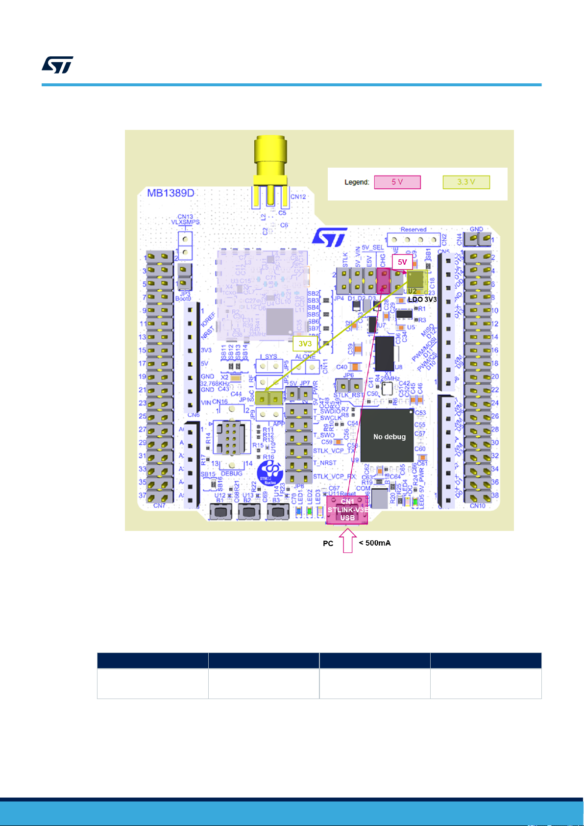
Figure 14. Power supply input from ST-LINK USB connector with 5 V USB charger
UM2592
Power supply
UM2592 - Rev 1
External power supply input from external 3.3 V
When the 3.3 V is provided by a shield board, it is interesting to use the 3.3 V (CN6 pin 4 or CN7 pin 16) directly
as power input (refer to Table 9 and Figure 15). In this case, the programming and debugging features are not
available, since the ST-LINK is not powered.
Table 9. External power sources: 3V3
Input power name
3V3
Connector pins Voltage range Maximum current
CN6 pin 4
CN7 pin 16
3 V to 3.6 V 1.3 A
page 21/49
Page 22

Figure 15. Power supply input from external 3V3
UM2592
Power supply
UM2592 - Rev 1
External power supply input STD_ALONE_5V (5 V, 500 mA maximum)
When the STM32WL Nucleo-64 board is power-supplied by STD_ALONE_5V (refer to Table 10 and Figure 16),
the jumper configuration must be the following: Jumper JP4 on pin 9-10 “ALONE”.
Table 10. External power sources: STD_ALONE_5V
Input power name
STD_ALONE_5V CN11 4.75 V to 5.25 V 500 mA
Connector pins Voltage range Maximum current
Refer to Section 6.4.1 for debugging when using an external power supply.
page 22/49
Page 23

Figure 16. Power supply input from STD_ALONE_5V (5V, 500mA maximum)
UM2592
Power supply
UM2592 - Rev 1
When the board is supplied with STD_ALONE_5V (on connector 11), then the STLINK-V3E debugger is not
supplied. Take care to correctly supply the board when using CN11. Pin 1 of CN11 is the STD_ALONE_5V supply
and pin 2 is the GND, as shown in Figure 17.
Figure 17. STD_ALONE_5V and GND pins on CN11
page 23/49
Page 24

To properly isolate the MCU STM32 WL from the STLINK-V3E debugger, it is recommended to remove the
following jumpers: the 6 jumpers of JP8 and the jumper of JP7. In this case, there is no current leakage coming
from the STLINK-V3E debugger in STM32WL current consumptions.
6.4.1 Debugging while using VIN or EXT as an external power supply
When powered by VIN or E5V, it is still possible to use the ST-LINK for programming or debugging, but it is
mandatory to power the board first using VIN or EXT, then to connect the USB cable to the PC. In this way, the
enumeration succeeds, thanks to the external power source.
The following power-sequence procedure must be respected:
1. Connect jumper JP4 between pins 5 and 6 for E5V or between pins 3 and 4 for VIN,
2. Connect the external power source to VIN or E5V,
3. Power on the external power supply 7 V < VIN < 12 V for VIN, or 5 V for E5V,
4. Check that the LED5 green LED is turned ON,
5. Connect the PC to the CN1 USB connector.
If this order is not respected, the board may be powered by USB first, then by VIN or E5V as the following risks
may be encountered:
1. If more than 300 mA current is needed by the board, the PC may be damaged or the current supplied can be
limited by the PC. As a consequence, the board is not powered correctly.
2. 300 mA is requested at enumeration so there is a risk that the request is rejected and the enumeration does
not succeed if the PC cannot provide such current. Consequently, the board is not power supplied and LED5
remains OFF.
UM2592
Clock sources
6.5 Clock sources
6.5.1 HSE clock (high-speed external clock)
There are two ways to configure the pins corresponding to the high-speed external clock (HSE):
• HSE on-board oscillator from X3 crystal: For typical frequencies and its capacitors and resistors, refer
to the STM32 microcontroller datasheet and the Oscillator design guide for STM8S, STM8A and STM32
microcontrollers application note (AN2867) for the oscillator design guide. The X3 crystal has the following
characteristics: 32 MHz, 10 pF load capacitance, 10 ppm. It is recommended to use NDK_NX2016SA
32MHz EXS00A-CS06465 manufactured by NDK. The configuration must be:
– X3 crystal (and X4 TCXO) soldered
– No C30 and no C38 as those capacitors are integrated into the STM32WL MCU
– SB20 OFF in order not to supply the TCXO
– C31 not fitted in order not to have 32MHz signal coming from the TCXO
– R39 and R40 ON to connect the X3 crystal to the STM32WL55 MCU
• HSE on-board oscillator from X4 TCXO (Default configuration): The X4 TCXO has the following
characteristics: 32MHz, 10pF load capacitance. It is recommended to use NT2016SF-32M-END5875A
manufactured by NDK. The configuration must be:
– X4 TCXO (and X3 crystal) soldered
– SB20 ON to supply the TCXO
– 10 pF C31 and 220 Ω R2 fitted to have a 32 MHz signal coming from the TCXO
– R39 and R40 OFF to isolate the X3 crystal from the STM32WL55 MCU
Note: Whatever the configuration is (X3 crystal or X4 TCXO), both X3 crystal and X4 TCXO are assembled on the
board in order not to have to solder or desolder either X3 or X4 to choose between X3 crystal or X4 TCXO
configuration.
UM2592 - Rev 1
page 24/49
Page 25

6.5.2 LSE clock (low-speed external clock) – 32.768 kHz
There are three ways to configure the pins corresponding to the low-speed clock (LSE):
• On-board oscillator (Default): X2 crystal. Refer to the Oscillator design guide for STM8S, STM8A
and STM32 microcontrollers application note (AN2867) as the oscillator design guide for STM32
microcontrollers. It is recommended to use NX3215SA-32.768kHz-EXS00A-MU00527 (32.768 kHz, 6 pF
load capacitance, 20 ppm) from NDK.
– SB11 and SB14 OFF
– SB12 and SB13 ON
• Oscillator from external PC14: from external oscillator through the pin 25 of CN7 connector. The
configuration must be:
– SB11 (and SB14 ON, but not necessary)
– SB12 and SB13 OFF
• LSE not used: PC14 and PC15 are used as GPIOs instead of the low-speed clock. The configuration must
be:
– SB11 and SB14 ON (to get them on CN7)
– SB12 and SB13 OFF
6.6 Board functions
UM2592
Board functions
6.6.1 LEDs
LED1 (USER LED)
This blue LED is a user LED connected to STM32WL I/O PB15. To light the LED LED1, a high-logic state “1” has
to be written in the corresponding GPIO PB15.
LED2 (USER LED)
This green LED is a user LED connected to STM32WL I/O PB9. To light the LED LED2, a high-logic state “1” has
to be written in the corresponding GPIO PB9.
LED3 (USER LED)
This red LED is a user LED connected to STM32WL I/O PB11. To light the LED LED3, a high-logic state “1” has to
be written in the corresponding GPIO PB11.
LED4 USB power fault (OC, overcurrent)
LED4 indicates that the board power consumption on USB ST-LINK exceeds 500 mA, consequently the user
must check the root cause of the overconsumption or power the board using an external power supply.
LED5 (5V_PWR)
The green LED indicates that the STM32WL part is powered and +5 V power is available on CN6 pin 5 and CN7
pin 18 if the jumper JP7 is fitted.
LED6 (STLINK-V3 COM LED)
UM2592 - Rev 1
The bicolor LED LED6 (green, red) provides information about STLINK-V3E communication status. LED6
indicates the communication progress between the PC and the STLINK-V3E, with the following setup:
• Blinking red: the first USB enumeration with the PC is taking place
• Red LED ON: when the initialization between the PC and STLINK-V3E is complete
• Blinking red or green: during programming and debugging with target
• Green LED ON: communication finished and successful
• Orange ON: communication failure
page 25/49
Page 26

6.6.2 Push-buttons
B1 (USER)
The user button is connected to the STM32WL I/O PA0 by default (WKUP1, SB16 ON, and SB15 OFF) or PC13
(WKUP2, SB15 ON, and SB16 OFF) of the STM32WL microcontroller.
B2 (USER)
The user button is connected to the STM32WL I/O PA1 of the STM32WL microcontroller.
B3 (USER)
The user button is connected to the STM32WL I/O PC6 of the STM32WL microcontroller.
B4 (RESET)
This push-button is connected to NRST and is used to RESET the STM32WL microcontroller.
6.6.3 RF overview
The STM32WL Nucleo-64 board embeds an RF 3-port switch (SP3T) to address, with the same board the
three modes: reception, high-power transmission, and low-power transmission. The choice between the two
transmission modes can be done dynamically, thanks to two DC switches controlled by FE_CTRL1 (GPIO from
STM32WL MCU):
• The transmission high-output power amplifier (PA HP) is supplied from the PA regulator (REG PA) up to
3.1 V. For this, the REG PA must be supplied directly from VDDSMPS.
• The transmission default low-output power amplifier (PA LP) can be supplied from the PA regulator (REG
PA) up to 1.35 V. For this, the REG PA must be supplied from the regulated VFBSMPS supply at 1.55 V.
The RF block diagram is displayed in Figure 18.
UM2592
Board functions
UM2592 - Rev 1
page 26/49
Page 27

Figure 18. RF block diagram
RF Rx path
RF Tx LP path
RF Tx HP path
32MHz HSE
SMPS part
STM32 WL transceiver
RF antenna matching
VDD_RF
UM2592
Board functions
Xtal
PB0-VDD_TCXO
TCXO
OSC_IN
OSC_OUT
VDDRF
VDDSMPS
Power
management
Reg PA
PA HP
PA LP
Rx
VLXSMPS
VFBSMPS
VDDRF1V55
VDDPA
VR_PA
DC
switch
RFO_HP
RFO_LP
RFI_P
RFI_N
DC
switch
matching
matching
matching
Rx
FE_CTRL1
Tx HP
Tx LP
SP3T
FE_CTRL3
FE_CTRL2
FE_CTRL1
RF
antenna
matching
The screwed and glue-fixed antennas to connect on the SMA connector and provided in the blister are:
• ANT-SS900 from LPRS company for NUCLEO-WL55JC1 (high band frequency)
• ANT-SS450-510 from LPRS company for NUCLEO-WL55JC2 (low band frequency)
Those antennas have been used for the different FCC/ISED/CE certifications. It is then mandatory to use those
referenced antennas (and only those) for radiated tests on the STM32WL Nucleo-64 boards.
6.6.4 Current consumption measurement (I_SoC)
Jumper JP1, labeled I_SoC, is used to measure the STM32WL microcontroller consumption by removing the
jumper and by connecting an ammeter. Their location in the power structure is shown in Figure 19.
1. JP1 ON. STM32WL is powered with 3V3 voltage (default)
2. JP4 OFF. An ammeter must be connected to measure the STM32WL current. If there is no ammeter, the
STM32 is not powered.
UM2592 - Rev 1
page 27/49
Page 28

Figure 19. JP1 and JP4 settings for current consumption measurement
JP2 (not fitted)
VDD_RF
SB28 (ON)
(VDD_RF)
UM2592
Board functions
SB27 (ON)
VDD_SYS
VDD_SYS
SB26
(ON)
JP5 (not fitted)
VDD_SYS
SB21
(ON)
SB24
(ON)
VDD_APP
VBAT
(VDD_SYS)
(VREF+)
(VBAT)
RF front-end
MCU STM32WL
(PB0_VDD_TCXO)
TCXO
RF part
5V_USB_STLK
5V_VIN
E5V
5V_USB_CHGR
STD_ALONE_5V
JP4
5V
U2
LDO
LD39050PU33R
3V3
JP1
ON
SB32 (ON)
JP9 OFF
VDD_MCU
AVDD
Note:
I_SoC (on VDD_MCU) is the current consumption of all the STM32WL MCU.
I_RF (on VDD_RF) is the current consumption of the RF part of the STM32WL MCU.
I_SYS (on VDD_SYS) is the current consumption of the rest of the STM32WL MCU (except I-RF).
So I_SoC = I_RF + I_SYS
We can evaluate the current consumption of the RF part of the STM32WL MCU by connecting an ammeter on
JP2. SB28 must be OFF in this case.
We can also evaluate the current consumption of the rest of the STM32WL MCU (VDD_SYS) by connecting an
ammeter on JP5. SB27 must be OFF in this case.
We can also evaluate the RF front-end current consumption (VDD_APP) by connecting an ammeter on JP9.
SB32 must be OFF in this case. This current consumption only concerns both NX3L1T3157GM DC switches (U3
and U4).
6.6.5 Virtual COM port (VCP): LPUART and USART
The STM32WL Nucleo-64 board offers the possibility to select which USART interface is connected to the
STLINK-V3E, ARDUINO® Uno V3 connector (CN9 pins 2 and 1), or to the ST morpho connector (CN10 pins 35
and 37).
The selection is done by setting the related solder bridges as detailed in Table 11 and Table 12.
Table 11. USART1 connection
Solder bridge configuration
SB6, SB10: ON
SB7, SB9, SB3, SB5: OFF
UM2592 - Rev 1
(1)
(1)
Feature
USART1 (PB6/PB7) connected to STLINK-V3E virtual COM
port.
page 28/49
Page 29

UM2592
Solder bridges
Solder bridge configuration
SB7, SB9: ON
1. The default configuration is shown in bold
SB6, SB10, SB2, SB4: OFF
(1)
USART1 (PB6/PB7) connected to Arduino™ (D1 & D0) and
ST morpho connector (CN10 pin 35 and 37).
Feature
(1)
Table 12. LPUART1 connection
Solder bridge configuration
SB3, SB5: ON
SB2, SB4, SB6, SB10: OFF
SB2, SB4: ON
1. The default configuration is shown in bold
SB3, SB5, SB7, SB9: OFF
(1)
LPUART1 (PA2/PA3) connected to STLINK-V3E Virtual
COM port.
LPUART1 (PA2/PA3) connected to ARDUINO® (D1 & D0) and
ST morpho connector (CN10 pin 35 and 37).
Feature
(1)
By default:
• Communication between the target STM32WL and the STLINK-V3E MCU is enabled on LPUART1 to
support the Virtual COM port.
• Communication between the target STM32WL and ARDUINO® (and ST morpho) connectors is enabled on
USART1.
6.7
Solder bridges
All the 31 solder bridges are located on the STM32WL Nucleo-64 board.
All the solder bridges present on the STM32WL Nucleo-64 board are used to configure several I/Os and power
supply pins for compatibility of features and pinout with the target STM32WL supported.
Table 13. Solder bridge configuration
Solder bridge control
3.3 V LDO
output
PA2
LPUART1 TX
PA3
LPUART1 RX
PB6
USART1 TX
Solder
bridge (SB)
SB1
SB2
SB3
SB4
SB5
SB6
State
(1)
Description
(1)
ON U2 LDO output provides 3.3 V
OFF
U2 LDO output does NOT provide 3.3V,
the user has to connect an external 3.3 V source.
ON ARD_D1_TX connected to LPUART1 TX PA2
OFF ARD_D1_TX not connected to LPUART1 TX PA2
ON STLINK_TX (T_VCP_TX) connected to LPUART1 TX PA2
OFF STLINK_TX (T_VCP_TX) not connected to LPUART1 TX PA2
ON ARD_D0_RX connected to LPUART1 RX PA3
OFF ARD_D0_RX not connected to LPUART1 RX PA3
ON STLINK_RX (T_VCP_RX) connected to LPUART1 RX PA3
OFF
STLINK_RX (T_VCP_RX) not connected to LPUART1 RX
PA3
ON STLINK_TX (T_VCP_TX) connected to USART1 TX PB6
OFF
STLINK_TX (T_VCP_TX) not connected to USART1 TX
PB6
UM2592 - Rev 1
page 29/49
Page 30

UM2592
Solder bridges
Solder bridge control
bridge (SB)
PB6
USART1 TX
T_SWO on PB3 SB8
PB7
USART1 RX
LSE CLK
SB12 / SB13
selection
B1 User button
SP3T VDD supply SB18
BOOT0/PH3 on STmorpho
connector
32 MHz TCXO supply SB20
VBAT SB21
VFBSMPS SB22
VDDSMPS SB23
VDDA / VREF+ supply SB24
Solder
SB7
SB9
SB10
SB11
SB14
SB15
SB16
SB19
State
(1)
Description
(1)
ON ARD_D1_TX connected to USART1 TX PB6
OFF ARD_D1_TX not connected to USART1 TX PB6
ON T_SWO connected to PB3
OFF T_SWO not connected to PB3 and isolated from ARD_D3
ON ARD_D0_RX connected to USART1 RX PB7
OFF ARD_D0_RX not connected to USART1 RX PB7
ON STLINK_RX (T_VCP_RX) connected to USART1 RX PB7
OFF
ON
STLINK_RX (T_VCP_RX) not connected to USART1 RX
PB7
PC14-OSC32_IN connected to ST morpho connector I/O
usage (CN7 pin 25)
OFF PC14-OSC32_IN not connected to ST morpho connector
ON LSE provided by external LSE 32.768kHz CLK X2
OFF LSE not provided by external LSE 32.768kHz CLK X2
ON
OFF
PC15-OSC32_OUT connected to ST morpho connector I/O
usage (CN7 pin 27)
PC15-OSC32_OUT not connected to ST morpho
connector
ON User button connected to PC13
OFF User button not connected to PC13
ON User button connected to PA0
OFF User button not connected to PA0
ON VDD supplied with FE_CTRL3 (STM32WL IO PC3)
OFF VDD not connected to FE_CTRL3 (STM32WL IO PC3)
ON
OFF
BOOT0/PH3 connected to ST Morpho connector CN7 pin
7
BOOT0/PH3 not connected to ST Morpho connector CN7 pin
7
ON 32 MHz TCXO supplied by PB0-VDD_TCXO (to STM32WL)
OFF
32 MHz TCXO disconnected to PB0-VDD_TCXO (to
STM32WL)
ON VBAT (pin A8 of STM32WL) powered by VDD_SYS
OFF
ON
OFF
ON
OFF
VBAT (pin A8 of STM32WL) supplied separately (through
VBAT on ST morpho connector CN7 pin 33)
VFBSMPS (pin B2 of STM32WL) connected to
VDDRF1V55 (pin F7 of STM32WL)
VFBSMPS (pin B2 of STM32WL) disconnected from
VDDRF1V55 (pin F7 of STM32WL) for current probing
VDDSMPS (pin A2 of STM32WL) connected to VDDRF (pin
E8 of STM32WL)
VDDSMPS (pin A2 of STM32WL) disconnected from VDDRF
(pin E8 of STM32WL) for current probing
STM32WL VDDA/VREF+ supplied by VDD_SYS through
ON
SMD ferrite bead L14. Be careful not to provide an
external AVDD supply if SB26 is fitted.
UM2592 - Rev 1
page 30/49
Page 31

UM2592
Solder bridges
Solder bridge control
Solder
bridge (SB)
VDDA / VREF+ supply SB24
IOREF and 3V3 connection SB25
VDDA / VREF+ supply SB26
I_SYS current probing SB27
I_RF current probing SB28
IOREF and VDD_MCU
connection
SB29
PB0 on ST morpho connector SB30
PB3 on morpho SB31
I_APP current probing SB32
1. The default SB state is in bold.
State
(1)
Description
(1)
STM32WL VDDA/VREF+ disconnected from VDD_SYS. So
OFF
STM32WL VDDA/VREF+ must be supplied externally by
AVDD.
ON
IOREF connected to the 3V3 power supply. Be careful to
remove SB29 to avoid voltage supply conflict with VDD_MCU.
OFF IOREF not connected to 3V3 power supply
ON
STM32WL VDDA/VREF+ supplied externally by AVDD (so
SB24 must not be fitted to avoid supply conflict)
STM32WL VDDA/VREF+ disconnected from AVDD. So SB24
OFF
must be fitted to supply properly STM32WL VDDA/VREF+
pins.
ON VDD_SYS generated from VDD_MCU
OFF For I_SYS current probing on JP5 jumper
ON VDD_RF generated from VDD_MCU
OFF For I_RF current probing on JP2 jumper
IOREF connected to the VDD_MCU power supply. Be
ON
careful to remove SB25 to avoid voltage supply conflict
with 3V3
OFF IOREF not connected to VDD_MCU power supply
ON PB0 connected to ST morpho connector (CN10 pin 22)
OFF PB0 not connected to ST morpho connector
ON PB3 connected to Arduino™ D3
OFF PB3 not connected to Arduino™ D3
ON RF front-end supply VDD_APP generated from VDD_MCU
OFF For I_APP current probing on JP9 jumper
UM2592 - Rev 1
page 31/49
Page 32

7 Board connectors
Several connectors are implemented on the STM32WL Nucleo-64 board.
7.1 CN1 STLINK-V3E USB Micro-B connector
The CN1 USB Micro-B connector is used to connect the embedded STLINK-V3E to a PC for programming and
debugging purposes.
Figure 20. USB Micro-B connector CN23 (front view)
UM2592
Board connectors
Table 14. USB Micro-B connector CN23 (front view)
Connector Pin number Pin name Signal name STLINK-V3EMCU pin Functions
1
2 DM USB_DEV_HS_CN_N R14 USB differential pair N
CN1
3 DP USB_DEV_HS_CN_P R15 USB differential pair P
4 ID - - -
5 GND - - GND
7.2 CN16 MIPI10 connector
Figure 21. MIPI10 debugging connector CN16 (top view)
V
BUS
5V_USB_CHGR - 5 V Power
UM2592 - Rev 1
The MIPI10 connector is implemented with a footprint compatible with the STDC14 footprint. The related pinout
for the MIPI10 connector is listed in Table 15.
page 32/49
Page 33

Table 15. CN16 MIPI10 connector pinout (STDC14 pinout compatible)
Connector Pin number Description Pin number Description
1 - 2 -
3 VDD (3V3) 4 T_SWDIO (PA13)
5 GND 6 T_SWCLK (PA14)
CN16
7 KEY (connected to GND) 8 T_SWO (PB3)
9 - 10 T_JTDI (PA15)
11
13 T_VCP_RX (PA3 by default or PB7) 14 T_VCP_TX (PA2 by default or PB6)
GNDDetect (connected to GND through
7.3 CN12 SMA connector
CN12 50 Ω SMA connector is available on the STM32WL Nucleo-64 board.
a 100 Ω resistor)
UM2592
CN12 SMA connector
12 T_NRST
Figure 22. CN12 SMA connector
By default, the output of the RF part is on the CN12 SMA connector.
Table 16. SMA connector pinout
Connector Pin number Description
1 RF path
2 GND
CN12
3 GND
4 GND
5 GND
7.4
UM2592 - Rev 1
CN5, CN6, CN8, and CN9 ARDUINO® Uno V3 connectors
The CN5, CN6, CN8, and CN9 ARDUINO® connectors (see Figure 23) are female connectors compatible with the
ARDUINO® standard. Most shields designed for ARDUINO® can fit with the STM32WL Nucleo-64 board.
The ARDUINO® connectors on the STM32WL Nucleo-64 board support the ARDUINO® Uno V3.
page 33/49
Page 34

CN5, CN6, CN8, and CN9 ARDUINO® Uno V3 connectors
Figure 23. ARDUINO® connectors
UM2592
Note:
The related pinout for the ARDUINO® connector is listed in Table 17.
ARDUINO® Uno V3 D0 and D1 signals are connected by default on USART1 (MCU I/O PB6 and PB7). For
details about how to modify the UART interface, refer to Section 6.6.5 .
Table 17. ARDUINO® connectors pinout
Connector
CN6
CN8
Pin number Pin name Signal name
1 NC - - Reserved for test
2 IOREF - - I/O reference
3 NRST T_NRST NRST RESET
4 3V3 - - 3.3 V input/output
5 5V - - 5 V output
6 GND - - GND
7 GND - - GND
8 VIN - - 7 V - 12 V input power
1 A0 ADC PB1 ADC1_IN5
2 A1 ADC PB2 ADC1_IN4
STM32 pin
(1)
Function
(1)
UM2592 - Rev 1
page 34/49
Page 35

UM2592
CN5, CN6, CN8, and CN9 ARDUINO® Uno V3 connectors
Connector Pin number Pin name Signal name
3 A2 ADC PA10 ADC1_IN6
CN8
4 A3 ADC PB4 ADC1_IN3
5 A4 ADC PB14 ADC1_IN1 / I2C3_SDA
6 A5 ADC PB13 ADC1_IN0 / I2C3_SCL
1 D8 ARD_D8 PC2 IO
2 PWM / D9 ARD_D9 PA9 TIM1_CH2
3 PWM /CS / D10 ARD_D10 PA4 LPTIM1_OUT / SPI1_NSS
4 PWM / MOSI / D11 ARD_D11 PA7 TIM17_CH1 / SPI1_MOSI
CN5
5 MISO / D12 ARD_D12 PA6 SPI1_MISO
6 SCK / D13 ARD_D13 PA5 SPI1_SCK
7 GND - - GND
8 AVDD AVDD AVVD / VREF+ Voltage reference
9 SDA / D14 ARD_D14 PA11 I2C1_SDA
10 SCL / D15 ARD_D15 PA12 I2C1_SCL
1 D7 ARD_D7 PC1 IO
2 PWM / D6 ARD_D6 PB10 TIM2_CH3
3 PWM/D5 ARD_D5 PB8 TIM16_CH1
4 D4 ARD_D4 PB5 IO
CN9
5 PWM / D3 ARD_D3 PB3 TIM2_CH2
6 D2 ARD_D2 PB12 IO
7 TX / D1 ARD_D1 PA2 / PB6
8 RX / D0 ARD_D0 PA3 / PB7
1. Default configuration is in bold.
STM32 pin
(1)
LPUSART1_TX /
USART1_TX
LPUSART1_RX /
USART1_RX
Function
(1)
UM2592 - Rev 1
page 35/49
Page 36

7.5 CN7 and CN10 ST morpho connectors
CN7 and CN10 ST morpho connectors are male pin headers accessible on both sides of the board. All signals
and power pins of the STM32WL MCU are available on the morpho connectors. These connectors can also be
probed by an oscilloscope, logical analyzer, or voltmeter.
Figure 24. ST morpho connectors
UM2592
CN7 and CN10 ST morpho connectors
Note: The D0 and D1 signals are connected by default to USART1 (MCU I/O PB6 and PB7). Refer to
Section 6.6.5 for details about how to modify the UART interface.
Table 18 shows the pin assignment of each STM32WL I/O on the ST morpho connector.
Table 18. Pin assignment of the ST morpho connectors
CN7 odd pins
Pin nbr Pin name Pin nbr
1 NC 2 NC 1 PA0 2 PC4
3 NC 4 NC 3 PA12 4 PC5
5 VDD_MCU 6 E5V 5 PA11 6 NC
7 BOOT0 8 GND 7 AVDD 8
9 NC 10 NC 9 GND 10 NC
UM2592 - Rev 1
CN7 even pins CN10 odd pins CN10 even pins
Pin name
(1)
Pin nbr
Pin name
(1)
Pin nbr Pin name
5V_USB_CHGR
page 36/49
(2)
Page 37

UM2592
CN7 and CN10 ST morpho connectors
CN7 odd pins CN7 even pins CN10 odd pins CN10 even pins
Pin nbr Pin name Pin nbr
Pin name
(1)
Pin nbr
Pin name
11 NC 12 IOREF 11 PA5 12 PC6
13
15
PA13
PA14
(3)
(3)
14 NRST 13 PA6 14 PC0
16 3V3 15 PA7 16 PA8
17 PA15 18 5V 17 PA4 18 NC
19 GND 20 GND 19 PA9 20 GND
21 NC 22 GND 21 PC2 22 PB0
23 PC13 24 VIN 23 PC1 24 NC
25 PC14 26 NC 25 PB10 26 PB9
27 PC15 28 PB1 27 PB8 28 PB15
29 NC 30 PB2 29 PB5 30 PB11
31 NC 32 PA10 31 PB3 32 AGND
33 VBAT 34 PB4 33 PB12 34 NC
35 NC 36 PB14 35 PB6 / PA2 36 PA1
37 NC 38 PB13 37 PB6 / PA3 38 PC3
1. Default configuration in bold.
2. 5V_USB_CHGR is the 5 V power from the STLINK-V3E USB connector that rises first. It rises before the 5 V rising on the
board.
3. PA13 and PA14 are shared with SWD signals connected to STLINK-V3E. It is not recommended to use them as I/O pins.
(1)
Pin nbr Pin name
UM2592 - Rev 1
page 37/49
Page 38

8 STM32WL Nucleo-64 board information
8.1 Product marking
The sticker located on the top or bottom side of the PCB board shows the information about product identification
such as board reference, revision, and serial number.
The first identification line has the following format: “MBxxxx-Variant-yzz”, where “MBxxxx” is the board reference,
“Variant” (optional) identifies the mounting variant when several exist, "y" is the PCB revision and "zz" is the
assembly revision: for example B01.
The second identification line is the board serial number used for traceability.
Evaluation tools marked as “ES” or “E” are not yet qualified and therefore not ready to be used as reference
design or in production. Any consequences deriving from such usage will not be at ST charge. In no event, ST will
be liable for any customer usage of these engineering sample tools as reference designs or in production.
“E” or “ES” marking examples of location:
• On the targeted STM32 that is soldered on the board (For an illustration of STM32 marking, refer to the
STM32 datasheet “Package information” paragraph at the www.st.com website).
• Next to the evaluation tool ordering part number that is stuck or silk-screen printed on the board.
8.2 Board revision history
UM2592
STM32WL Nucleo-64 board information
Revision D04
The revision D04 of the MB1389 is the initially released version.
8.3 Known limitations
Revision D04
On MB1389 revision D04, the maximum output power is limited to 19.7 dBm to fulfill FCC/IC/CE requirements. An
output power higher than 19.7 dBm at the antenna is prohibited.
UM2592 - Rev 1
page 38/49
Page 39

UM2592
STM32WL Nucleo-64 I/O assignment
Appendix A STM32WL Nucleo-64 I/O assignment
Table 19. STM32WL Nucleo-64 I/O assignment
Pin Pin name Signal or label
A1 VSSSMPS VSSSMPS GND of LDO/SMPS step-down converter
A2 VDDSMPS VDDSMPS
A4 PA14 T_SWCLK T_SWCLK
A5 VDDA VDDA Analog voltage supply
A7 VDD VDD VDD voltage supply
A8 VBAT VBAT VBAT voltage supply
A9 PA12 PA12 ARD_D15 - I2C2_SCL
B1 VLXSMPS VLXSMPS VLXSMPS pin of SMPS step-down converter
B2 VFBSMPS VFBSMPS 1V55 provided by the SMPS step-down converter
B3 PA15 T_JTDI T_JTDI
B4 PB15 PB15 LED1
B5 VREF+ VREF+ Input reference voltage for ADC
B6 PC14-OSC32_IN OSC32_IN / PC14 LSE_CLK / GPIO PC14
B7 VSS GND GND
B8 PA13 T_SWDIO T_SWDIO
B9 PA11 PA11 ARD_D14 - I2C2_SDA
C1 PB3 PB3 ARD_D3 - TIM2_CH2 / T_SWO
C2 PB4 PB4 ARD_A3 - ADC1_IN3
C3 PB7 LPUART1_RX ARD_D0 / STLINK_RX (T_VCP_RX)
C4 PB9 PB9 LED2
C5 PC15-OSC32_OUT OSC32_OUT / PC15 LSE CLK / GPIO PC15
C6 PB14 PB14 ARD_A4 - ADC1_IN1/I2C3_SDA
C7 PC13 PC13 GPIO PC13 / B1 user button
C8 PA10 PA10 ARD_A2 - ADC1_IN6
D2 PB5 PB5 ARD_D4 - IO
D3 PB8 PB8 ARD_D5 - TIM16_CH1
D4 PC2 PC2 ARD_D8 - IO
D5 PC3 PC3 FE_CTRL3
D6 PA0 PA0 B1 user button / GPIO PA0
D7 PB13 PB13 ARD_A5 - ADC1_IN0/I2C3_SCL
D8 PB2 PB2 ARD_A1 - ADC1_IN4
D9 VSS GND GND
E1 PB6 LPUART1_TX ARD_D1 / STLINK_TX (T_VCP_TX)
E2 VDD VDD VDD voltage supply
E3 VSS GND GND
E4 PC5 PC5 FE_CTRL2
Main feature / optional feature / (SB)
External power supply of LDO/SMPS step-down
converter
(1)
UM2592 - Rev 1
page 39/49
Page 40

UM2592
STM32WL Nucleo-64 I/O assignment
Pin Pin name Signal or label
Main feature / optional feature / (SB)
E5 PA9 PA9 ARD_D9 - TIM1_CH2
E6 PB12 PB12 ARD_D2 - IO
E7 PB1 PB1 ARD_A0 - ADC1_IN5
E8 VDDRF VDDRF VDD supply for the RF part
E9 VDD VDD VDD voltage supply
F1 PC1 PC1 ARD_D7 - IO
F2 PC0 PC0 IO
F3 PC4 PC4 FE_CTRL1
F4 PA6 PA6 ARD_D12 - SPI1_MISO
F5 NRST T_NRST STM32WL RESET
F6 PB0-VDD_TCXO PB0-VDD_TCXO Supply voltage of TCXO / GPIO PB0
F7 VDDRF1V55 VDDRF1V55 External power supply for the radio
F8 OSC_OUT OSC_OUT HSE CLK
G2 PC6 PC6 B3 user button
G3 PA1 PA1 B2 user button
G4 PB11 PB11 LED3
G5 VSS GND GND
G6 VSSRF VSSRF GND for RF part
G7 VSSRF VSSRF GND for RF part
G8 VSSRF VSSRF GND for RF part
G9 OSC_IN OSC_IN HSE CLK
H1 PA3 LPUART_RX STLINK_RX (T_VCP_RX) / ARD_D0
H2 PA2 LPUART_TX STLINK_TX (T_VCP_TX) / ARD_D1
H3 PA7 PA7 ARD_D11 - TIM17_CH1/SPI1_MOSI
H4 PB10 PB10 ARD_D6 - TIM2_CH3
H5 VDD VDD VDD voltage supply
H6 VSSRF VSSRF GND for RF part
H7 RFI_N RFI_N RF receive input (differential N path)
H8 VDDPA VDDPA Input supply for PA regulator
H9 VR_PA VR_PA Regulated PA supply output
J1 PA4 PA4 ARD_D10 - LPTIM1_OUT/SPI1_NSS
J2 PA5 PA5 ARD_D13 - SPI1_SCK
J3 PA8 PA8 IO
J5 PH3 PH3 BOOT0
J6 RFI_P RFI_P RF receive input (differential P path)
J8 RFO_LP RFO_LP Transmit default power PA output
J9 RFO_HP RFO_HP Transmit high-power PA output
1. The default configuration is shown in bold.
(1)
UM2592 - Rev 1
page 40/49
Page 41

UM2592
Federal Communications Commission (FCC) and Innovation, Science and Economic Development Canada (ISED) Compliance Statements
Appendix B Federal Communications Commission (FCC) and Innovation,
Science and Economic Development Canada (ISED) Compliance Statements
B.1 FCC Compliance Statement
Part 15.19
This device complies with Part 15 of the FCC Rules. Operation is subject to the following two conditions: (1) this
device may not cause harmful interference, and (2) this device must accept any interference received, including
interference that may cause undesired operation.
Part 15.21
Any changes or modifications to this equipment not expressly approved by STMicroelectronics may cause
harmful interference and void the user's authority to operate this equipment.
Part 15.105
This equipment has been tested and found to comply with the limits for a Class B digital device, pursuant to part
15 of the FCC Rules. These limits are designed to provide reasonable protection against harmful interference
in a residential installation. This equipment generates uses and can radiate radio frequency energy and, if not
installed and used in accordance with the instruction, may cause harmful interference to radio communications.
However, there is no guarantee that interference will not occur in a particular installation. If this equipment does
cause harmful interference to radio or television reception which can be determined by turning the equipment off
and on, the user is encouraged to try to correct interference by one or more of the following measures:
• Reorient or relocate the receiving antenna.
• Increase the separation between the equipment and receiver.
• Connect the equipment into an outlet on circuit different from that to which the receiver is connected.
• Consult the dealer or an experienced radio/TV technician for help.
Note: Use only shielded cables.
B.2
Responsible party (in the USA)
Terry Blanchard
Americas Region Legal | Group Vice President and Regional Legal Counsel, The Americas
STMicroelectronics, Inc.
750 Canyon Drive | Suite 300 | Coppell, Texas 75019
USA
Telephone: +1 972-466-7845
Additional FCC and ISED Compliance Statements
ISED Licence-Exempt Radio Apparatus
This device contains license-exempt transmitter(s)/receiver(s) that comply with Innovation, Science and Economic
Development Canada’s license-exempt RSS(s). Operation is subject to the following two conditions:
1. This device may not cause interference.
2. This device must accept any interference, including interference that may cause undesired operation of the
device.
Appareils radio exempts de licence ISDE
L’émetteur/récepteur exempt de licence contenu dans le présent appareil est conforme aux CNR d’Innovation,
Sciences et Développement économique Canada applicables aux appareils radio exempts de licence.
L’exploitation est autorisée aux deux conditions suivantes :
1. L’appareil ne doit pas produire de brouillage ;
2. L'appareil doit accepter tout brouillage radioélectrique subi, même si le brouillage est susceptible d'en
compromettre le fonctionnement.
UM2592 - Rev 1
page 41/49
Page 42

UM2592
Additional FCC and ISED Compliance Statements
Radio Frequency (RF) Exposure Compliance of Radiocommunication Apparatus
To satisfy FCC and ISED RF Exposure requirements for mobile devices, a separation distance of 20 cm or more
should be maintained between the antenna of this device and persons during operation. To ensure compliance,
operation at closer than this distance is not recommended. This transmitter must not be co-located or operating in
conjunction with any other antenna or transmitter.
Pour satisfaire aux exigences FCC et ISDE concernant l'exposition aux champs RF pour les appareils mobiles,
une distance de séparation de 20 cm ou plus doit être maintenu entre l'antenne de ce dispositif et les personnes
pendant le fonctionnement. Pour assurer la conformité, il est déconseillé d'utiliser cet équipement à une distance
inférieure. Cet émetteur ne doit pas être co-situé ou fonctionner conjointement avec une autre antenne ou un
autre émetteur.
UM2592 - Rev 1
page 42/49
Page 43
UM2592
Déclaration de conformité CE simplifiée
Appendix C Déclaration de conformité CE simplifiée
Le soussigné, STMicroelectronics, déclare que l'équipement radioélectrique du type Nucleo MB1389D est
conforme à la directive 2014/53/UE. Le texte complet de la déclaration UE de conformité est disponible à
l'adresse internet suivante: www.st.com.
Bande de fréquence utilisée en transmission et puissance max rayonnée dans ces bandes :
Bande de fréquence : 865 MHz / 870 MHz
Puissance Max : 25 mW e.r.p
UM2592 - Rev 1
page 43/49
Page 44

Revision history
UM2592
Table 20. Document revision history
Date Version Changes
17-Nov-2020 1 Initial release.
UM2592 - Rev 1
page 44/49
Page 45

UM2592
Contents
Contents
1 Features...........................................................................2
2 Ordering information ..............................................................3
2.1 Codification ...................................................................3
3 Development environment .........................................................4
3.1 System requirements ...........................................................4
3.2 Development toolchains .........................................................4
3.3 Demonstration software .........................................................4
4 Conventions.......................................................................5
5 Quick start ........................................................................6
5.1 Getting started .................................................................6
6 Hardware layout and configuration.................................................8
6.1 PCB layout ....................................................................9
6.2 Mechanical drawing ...........................................................12
6.3 Embedded STLINK-V3E .......................................................12
6.3.1 Drivers ...............................................................13
6.3.2 STLINK-V3E firmware upgrade.............................................13
6.3.3 Using an external debug tool to program and debug the on-board STM32 ............13
6.4 Power supply .................................................................15
6.4.1 Debugging while using VIN or EXT as an external power supply ...................24
6.5 Clock sources ................................................................24
6.5.1 HSE clock (high-speed external clock) .......................................24
6.5.2 LSE clock (low-speed external clock) – 32.768 kHz .............................25
6.6 Board functions ...............................................................25
6.6.1 LEDs.................................................................25
6.6.2 Push-buttons...........................................................26
6.6.3 RF overview ...........................................................26
6.6.4 Current consumption measurement (I_SoC) ...................................27
6.6.5 Virtual COM port (VCP): LPUART and USART .................................28
6.7 Solder bridges ................................................................29
UM2592 - Rev 1
page 45/49
Page 46

UM2592
Contents
7 Board connectors ................................................................32
7.1 CN1 STLINK-V3E USB Micro-B connector ........................................32
7.2 CN16 MIPI10 connector ........................................................32
7.3 CN12 SMA connector..........................................................33
7.4 CN5, CN6, CN8, and CN9 ARDUINO® Uno V3 connectors ..........................33
7.5 CN7 and CN10 ST morpho connectors ...........................................36
8 STM32WL Nucleo-64 board information ...........................................38
8.1 Product marking ..............................................................38
8.2 Board revision history ..........................................................38
8.3 Known limitations .............................................................38
Appendix A STM32WL Nucleo-64 I/O assignment .....................................39
Appendix B Federal Communications Commission (FCC) and Innovation, Science and
Economic Development Canada (ISED) Compliance Statements ...................41
B.1 FCC Compliance Statement ....................................................41
B.2 Additional FCC and ISED Compliance Statements .................................41
Appendix C Déclaration de conformité CE simplifiée ..................................43
Revision history .......................................................................44
Contents ..............................................................................45
List of tables ..........................................................................47
List of figures..........................................................................48
UM2592 - Rev 1
page 46/49
Page 47

UM2592
List of tables
List of tables
Table 1. List of available products...............................................................3
Table 2. Codification explanation ............................................................... 3
Table 3. ON/OFF convention ..................................................................5
Table 4. Jumper configuration .................................................................6
Table 5. CN16 MIPI10 / STDC14 debug connector .................................................. 14
Table 6. External power sources: VIN (7 V - 12 V) .................................................. 18
Table 7. External power sources: E5V (5 V)....................................................... 19
Table 8. External power sources: 5V_CHGR (5 V) .................................................. 20
Table 9. External power sources: 3V3 ........................................................... 21
Table 10. External power sources: STD_ALONE_5V ................................................. 22
Table 11. USART1 connection ................................................................. 28
Table 12. LPUART1 connection ................................................................ 29
Table 13. Solder bridge configuration ............................................................ 29
Table 14. USB Micro-B connector CN23 (front view).................................................. 32
Table 15. CN16 MIPI10 connector pinout (STDC14 pinout compatible) .....................................33
Table 16. SMA connector pinout ............................................................... 33
Table 17.
Table 18. Pin assignment of the ST morpho connectors ............................................... 36
Table 19. STM32WL Nucleo-64 I/O assignment ..................................................... 39
Table 20. Document revision history ............................................................. 44
ARDUINO® connectors pinout .......................................................... 34
UM2592 - Rev 1
page 47/49
Page 48

UM2592
List of figures
List of figures
Figure 1. NUCLEO-WL55JC top view ...........................................................1
Figure 2. NUCLEO-WL55JC bottom view ........................................................ 1
Figure 3. Hardware block diagram .............................................................8
Figure 4. Top layout .......................................................................9
Figure 5. RF certification and UID64 stickers ..................................................... 10
Figure 6. Bottom layout .................................................................... 11
Figure 7. STM32WL Nucleo 73 board mechanical drawing (in millimeter) ................................. 12
Figure 8. USB composite device.............................................................. 13
Figure 9. Connecting an external debug tool to program the on-board STM32WL ............................14
Figure 10. STM32WL Nucleo-64 board power tree ..................................................16
Figure 11. Power supply input from STLINK-V3E USB connector with PC (5 V, 500 mA maximum)................. 17
Figure 12. Power supply input from VIN (from 7 V to 12 V, 800 mA maximum) ............................... 19
Figure 13. Power supply input from 5V_EXT (5 V, 500 mA maximum) ..................................... 20
Figure 14. Power supply input from ST-LINK USB connector with 5 V USB charger ........................... 21
Figure 15. Power supply input from external 3V3 ................................................... 22
Figure 16. Power supply input from STD_ALONE_5V (5V, 500mA maximum) ............................... 23
Figure 17. STD_ALONE_5V and GND pins on CN11 ................................................ 23
Figure 18. RF block diagram ................................................................. 27
Figure 19. JP1 and JP4 settings for current consumption measurement ................................... 28
Figure 20. USB Micro-B connector CN23 (front view) ................................................ 32
Figure 21. MIPI10 debugging connector CN16 (top view) ............................................. 32
Figure 22. CN12 SMA connector .............................................................. 33
Figure 23. ARDUINO® connectors ............................................................. 34
Figure 24. ST morpho connectors ............................................................. 36
UM2592 - Rev 1
page 48/49
Page 49

UM2592
IMPORTANT NOTICE – PLEASE READ CAREFULLY
STMicroelectronics NV and its subsidiaries (“ST”) reserve the right to make changes, corrections, enhancements, modifications, and improvements to ST
products and/or to this document at any time without notice. Purchasers should obtain the latest relevant information on ST products before placing orders. ST
products are sold pursuant to ST’s terms and conditions of sale in place at the time of order acknowledgement.
Purchasers are solely responsible for the choice, selection, and use of ST products and ST assumes no liability for application assistance or the design of
Purchasers’ products.
No license, express or implied, to any intellectual property right is granted by ST herein.
Resale of ST products with provisions different from the information set forth herein shall void any warranty granted by ST for such product.
ST and the ST logo are trademarks of ST. For additional information about ST trademarks, please refer to www.st.com/trademarks. All other product or service
names are the property of their respective owners.
Information in this document supersedes and replaces information previously supplied in any prior versions of this document.
© 2020 STMicroelectronics – All rights reserved
UM2592 - Rev 1
page 49/49
 Loading...