

Wide Bandwidth Dual Bipolar Operational Amplifier
1
2
3
45
6
7
8
-
+
-
+
Output 1
Inverting input 1
Non-inverting input 1
V
CC
V
CC
Output 2
Inverting input 2
Non-inverting input 2
-
+
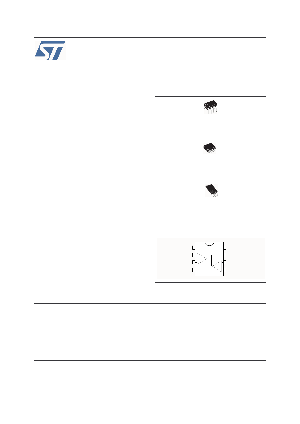
■ Internally compensated
■ Short-circuit protection
■ Gain and phase match between amplifier
■ Low power consumption
■ Pin-to-pin compatible with MC1458/LM358
■ Gain bandwidth product (at 100kHz): 5.5MHz
Description
The MC4558 is a high performance monolithic
dual operational amplifier.
The circuit combines all the outstanding features
of the MC1458 and, in addition possesses three
times the unity gain bandwidth of the industry
standard.
MC4558
N
DIP8
(Plastic Package)
D
SO-8
(Plastic Micropackage)
P
TSSOP8
(Thin Shrink Small Outline Package)
Pin connections (top view)
Order Codes
Part Number Temperature Range Package Packing Marking
MC4558CN
MC4558CD/CDT SO-8 Tube or Tape & Reel
0°C to +70°C
MC4558CPT TSSOP8 Tape & Reel
MC4558IN
MC4558ID/IDT SO-8 Tube or Tape & Reel
MC4558IPT
-40°C to +105°C
(Thin Shrink Outline Package)
October 2005 1/10
DIP8 Tube MC4558CN
4558C
DIP8 Tube MC4558IN
TSSOP8
Tape & Reel
4558I
www.st.com
Rev 2
10
Absolute Maximum Ratings MC4558
1 Absolute Maximum Ratings
Table 1. Key parameters and their absolute maximum ratings
Symbol Parameter MC4558I MC4558C Unit
V
V
V
Supply Voltage ±22 V
CC
(1)
Input Voltage ±15 V
i
(2)
Differential Input Voltage ±30 V
id
P
Power Dissipation 680 mW
tot
Output Short Circuit Duration Infinite
T
Operating Free-Air Temperature Range -40 to +105 0 to +70 °C
oper
Thermal Resistance Junction to Ambient
R
thja
ESD
SO-8
TSSOP8
DIP8
HBM: Human Body Model
MM: Machine Model
(4)
(3)
125
120
85
500
500
°C/W
CDM: Charged Device Model 1500
1. Input voltage are with respect to the midpoint between Vcc+ and Vcc-. Its value must never exceed 15V or the
magnitude of Vcc, whichever is less.
2. Differential voltages are the non-inverting input terminal with respect to the inverting input terminal.
3. Human body model, 100pF discharged through a 1.5kΩ resistor into pin of device.
4. Machine model ESD, a 200pF cap is charged to the specified voltage, then discharged directly into the IC with
no external series resistor (internal resistor < 5Ω), into pin to pin of device.
V
Table 2. Operating conditions
Symbol Parameter Min. Max. Unit
V
2/10
Supply voltage ±2 ±20 V
CC
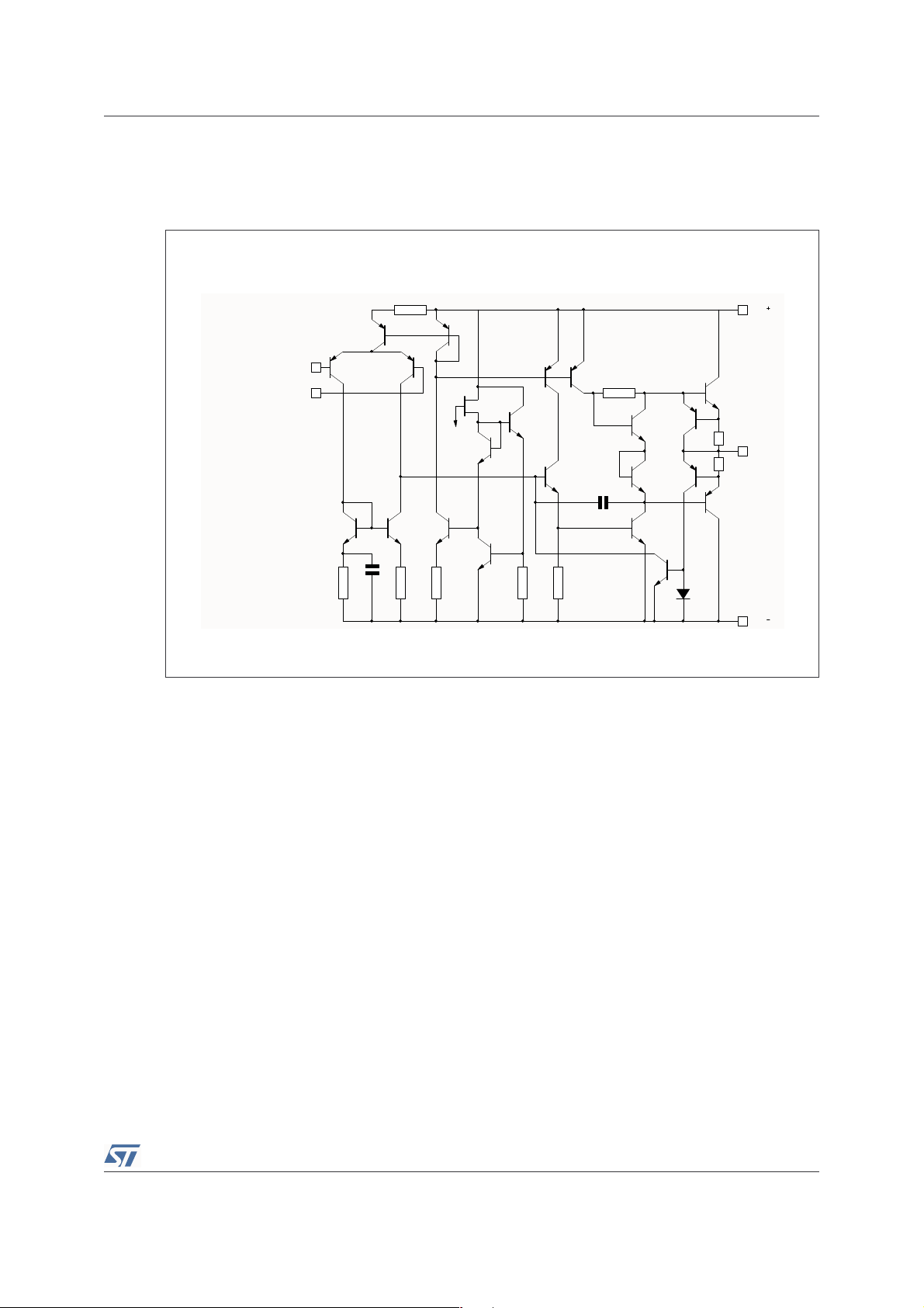
MC4558 Typical Application Schematic
3.1k
Ω
Inverting input
Non-inverting input
7.1k
Ω
87pF
7.1kΩ
480
Ω
4.2k
Ω
36k
Ω
10pF
150Ω
25Ω
Output
25
Ω
V
CC
V
CC
2 Typical Application Schematic
Figure 1. Schematic diagram (1/2MC4558)
3/10

Electrical Characteristics MC4558
3 Electrical Characteristics
Table 3. Electrical characteristics for VCC = ±15V, T
= 25°C (unless otherwise specified)
amb
Symbol Parameter Min. Typ. Max. Unit
Input Offset Voltage (Rs ≤ 10kΩ)
T
T
amb
min
= +25°C
. ≤ T
amb
≤ T
156mV
max.
V
io
Input Offset Current
T
T
amb
min
= +25°C
. ≤ T
amb
≤ T
max.
20 100
200
I
io
Input Bias Current
= +25°C
I
ib
T
T
amb
min
. ≤ T
amb
≤ T
max.
50 400
500
Large Signal Voltage Gain (RL = 2kΩ, Vo = ±10V)
T
A
vd
SVR
= +25°C
amb
T
min
. ≤ T
amb
≤ T
max.
Supply Voltage Rejection Ratio (R
T
= +25°C
amb
T
min
. ≤ T
amb
≤ T
max.
≤ 10kΩ)
s
50
25
77
77
200 V/mV
90 dB
Supply Current, all amplifiers, no load
T
T
amb
min
= +25°C
. ≤ T
amb
≤ T
max.
2.3 4.5
6
I
CC
Input Common Mode Voltage Range
T
V
icm
CMR
I
os
= +25°C
amb
T
min
. ≤ T
amb
≤ T
max.
Common-mode Rejection Ratio (R
T
= +25°C
amb
T
min
. ≤ T
amb
≤ T
max.
≤ 10kΩ)
s
±12
±12
70
70
90 dB
Output Short Circuit Current 10 20 40 mA
Output Voltage Swing
T
= +25°C RL = 10kΩ
K
V
SR
t
OV
R
amb
R
= 2kΩ
o
L
T
min
R
L
. ≤ T
= 2kΩ
amb
≤ T
max. RL
= 10kΩ
±12
±10
±12
±10
Slew Rate
V
= ±10, RL = 2kΩ, CL = 100pF, T
i
Rise Time
r
V
= ±20mV, RL = 2kΩ, CL = 100pF, T
i
Overshoot
V
= ±20mV, RL = 2kΩ, CL = 100pF, T
i
Input Resistance 0.3 2 MΩ
i
= 25°C, unity gain
amb
= 25°C, unity gain
amb
= 25°C, unity gain
amb
1.5 2.2
±14
±13 V
0.3
15
nA
nA
mA
V
V/µs
µs
%
4/10

Electrical Characteristics MC4558
Table 3. Electrical characteristics for VCC = ±15V, T
= 25°C (unless otherwise specified)
amb
Symbol Parameter Min. Typ. Max. Unit
C
R
Input Capacitance 1.4 pF
i
Output Resistance 75 Ω
o
B Unity Gain Bandwidth 2.8 MHz
GBP
THD
e
V
O1/VO2
Gain Bandwidth Product
V
= 10mV, RL = 2kΩ, CL = 100pF, f = 100kHz, T
i
amb
= 25°C
5.5
Total Harmonic Distortion
f = 1kHz, A
Equivalent Input Noise Voltage (RS = 100Ω, f = 1kHz)
n
= 20dB, RL = 2kΩ, Vo = 2Vpp, CL = 100pF, T
v
amb
= 25°C
0.008
12
Channel Separation 120 dB
MHz
%
nV
-----------Hz
5/10

Electrical Characteristics MC4558
OSCILLOSCOPE
OSCILLOSCOPE
V
I
C
L
R
L
Figure 2. Transient response test circuit Figure 3. Positive output voltage swing vs.
load resistance
Figure 4. Open loop frequency
response
Figure 5. Negative output voltage swing
vs. load resistance
Figure 6. Phase margin vs. frequency Figure 7. Power bandwidth
6/10

Package Mechanical Data MC4558
4 Package Mechanical Data
In order to meet environmental requirements, ST offers these devices in ECOPACK® packages.
These packages have a Lead-free second level interconnect. The category of second level
interconnect is marked on the package and on the inner box label, in compliance with JEDEC
Standard JESD97. The maximum ratings related to soldering conditions are also marked on
the inner box label. ECOPACK is an ST trademark. ECOPACK specifications are available at:
www.st.com
4.1 DIP8 package
.
Plastic DIP-8 MECHANICAL DATA
DIM.
A 3.3 0.130
a1 0.7 0.028
B 1.39 1.65 0.055 0.065
B1 0.91 1.04 0.036 0.041
b 0.5 0.020
b1 0.38 0.5 0.015 0.020
D 9.8 0.386
E 8.8 0.346
e 2.54 0.100
e3 7.62 0.300
e4 7.62 0.300
F 7.1 0.280
I 4.8 0.189
L 3.3 0.130
Z 0.44 1.6 0.017 0.063
MIN. TYP MAX. MIN. TYP. MAX.
mm. inch
7/10
P001F

Package Mechanical Data MC4558
4.2 SO-8 package
SO-8 MECHANICAL DATA
DIM.
A 1.35 1.75 0.053 0.069
A1 0.10 0.25 0.04 0.010
A2 1.10 1.65 0.043 0.065
B 0.33 0.51 0.013 0.020
C 0.19 0.25 0.007 0.010
D 4.80 5.00 0.189 0.197
E 3.80 4.00 0.150 0.157
e 1.27 0.050
H 5.80 6.20 0.228 0.244
h 0.25 0.50 0.010 0.020
L 0.40 1.27 0.016 0.050
k ˚ (max.)
ddd 0.1 0.04
MIN. TYP MAX. MIN. TYP. MAX.
mm. inch
8
8/10
0016023/C

Package Mechanical Data MC4558
4.3 TSSOP8 package
TSSOP8 MECHANICAL DATA
DIM.
MIN. TYP MAX. MIN. TYP. MAX.
A 1.2 0.047
A1 0.05 0.15 0.002 0.006
A2 0.80 1.00 1.05 0.031 0.039 0.041
b 0.19 0.30 0.007 0.012
c 0.09 0.20 0.004 0.008
D 2.90 3.00 3.10 0.114 0.118 0.122
E 6.20 6.40 6.60 0.244 0.252 0.260
E1 4.30 4.40 4.50 0.169 0.173 0.177
e 0.65 0.0256
K0˚ 8˚0˚ 8˚
L 0.45 0.60 0.75 0.018 0.024 0.030
L1 1 0.039
mm. inch
9/10
0079397/D

Revision History MC4558
5 Revision History
Date Revision Changes
Oct. 2001 1 Initial release.
The following changes were made in this revision:
Oct. 2005 2
Table 2.: Operating conditions on page 2
–
max.
– Addition of supplementary data in
absolute maximum ratings on page 2
– Minor grammatical and formatting changes throughout.
updated with Vcc min. and
Table 1.: Key parameters and their
Information furnished is believed to be accurate and reliable. However, STMicroelectronics assumes no responsibility for the consequences
of use of such information nor for any infringement of patents or other rights of third parties which may result from its use. No license is
granted by implication or otherwise under any patent or patent rights of STMicroelectronics. Specifications mentioned in this publication are
subject to change without notice. This publication supersedes and replaces all information previously supplied. STMicroelectronics products
are not authorized for use as critical components in life support devices or systems without express written approval of STMicroelectronics.
The ST logo is a registered trademark of STMicroelectronics.
All other names are the property of their respective owners
© 2005 STMicroelectronics - All rights reserved
STMicroelectronics group of companies
Australia - Belgium - Brazil - Canada - China - Czech Republic - Finland - France - Germany - Hong Kong - India - Israel - Italy - Japan -
Malaysia - Malta - Morocco - Singapore - Spain - Sweden - Switzerland - United Kingdom - United States of America
www.st.com
10/10
 Loading...