

Page 1
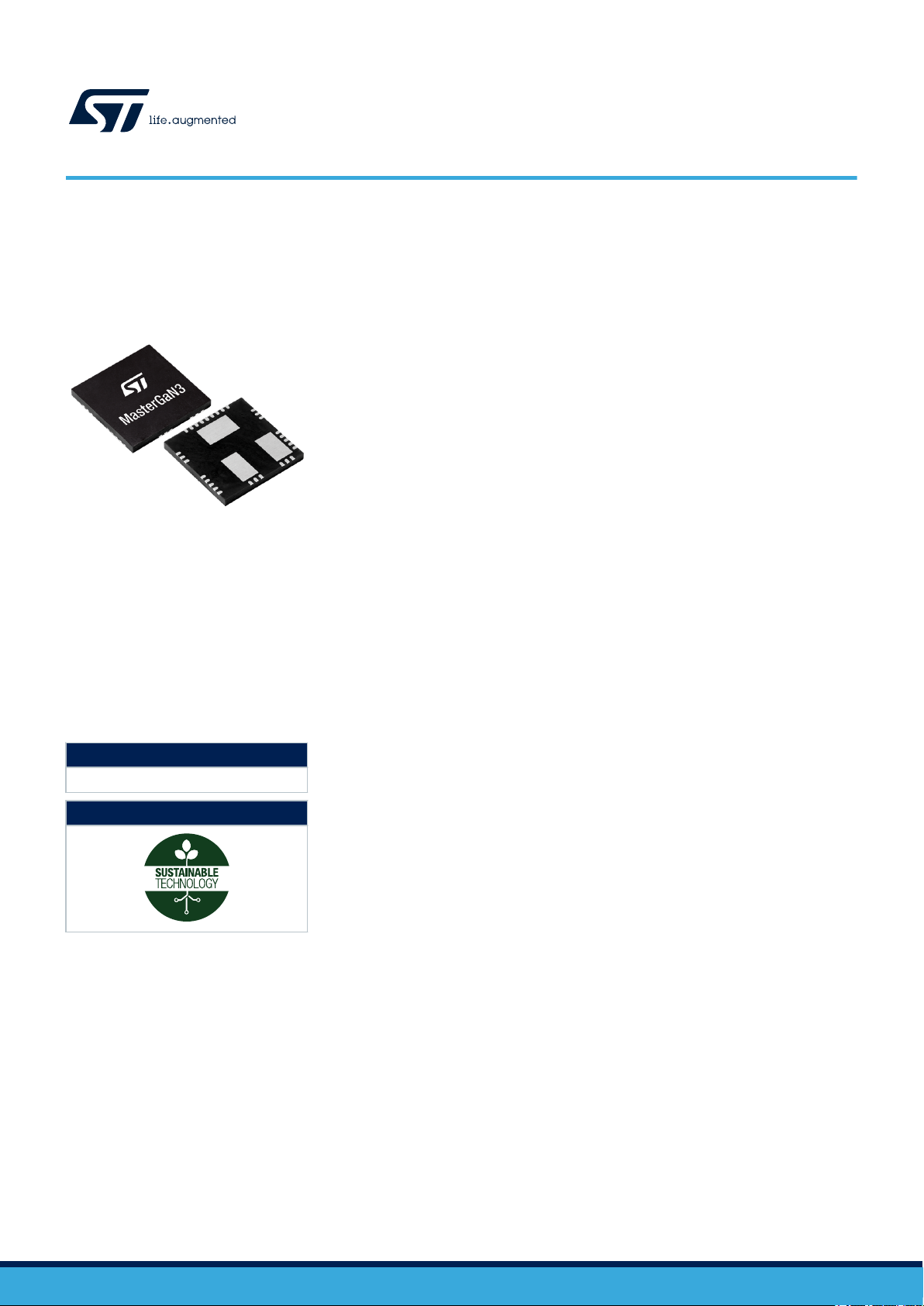
MASTERGAN3
Datasheet
High power density 600 V Half bridge driver with two enhancement mode
GaNHEMT
Features
• 600 V system-in-package integrating half-bridge gate driver and high-voltage
power GaN transistors in asymmetrical configuration:
– QFN 9 x 9 x 1 mm package
– R
– I
DS(MAX)
• Reverse current capability
• Zero reverse recovery loss
• UVLO protection on low-side and high-side
• Internal bootstrap diode
• Interlocking function
• Dedicated pin for shutdown functionality
• Accurate internal timing match
• 3.3 V to 15 V compatible inputs with hysteresis and pull-down
• Overtemperature protection
• Bill of material reduction
• Very compact and simplified layout
• Flexible, easy and fast design.
= 225 mΩ (LS) + 450 mΩ (HS)
DS(ON)
= 6.5 A (LS) + 4 A (HS)
Product status link
MASTERGAN3
Product label
Application
• Switch-mode power supplies
• Chargers and adapters
• High-voltage PFC, and DC-DC converters
Description
The MASTERGAN3 is an advanced power system-in-package integrating a gate
driver and two enhancement mode GaN transistors in asymmetrical half‑bridge
configuration.
The integrated power GaNs have 650 V drain‑source blocking voltage and R
of 225 mΩ and 450 mΩ for Low side and High side respectively, while the high
side of the embedded gate driver can be easily supplied by the integrated bootstrap
diode, while the high side of the embedded gate driver can be easily supplied by the
integrated bootstrap diode.
The MASTERGAN3 features UVLO protection on both the lower and upper
driving sections, preventing the power switches from operating in low efficiency
or dangerous conditions, and the interlocking function avoids cross-conduction
conditions.
The input pins extended range allows easy interfacing with microcontrollers, DSP
units or Hall effect sensors.
The MASTERGAN3 operates in the industrial temperature range, -40°C to 125°C.
The device is available in a compact 9x9 mm QFN package.
DS(ON)
DS13724 - Rev 1 - May 2021
For further information contact your local STMicroelectronics sales office.
www.st.com
Page 2
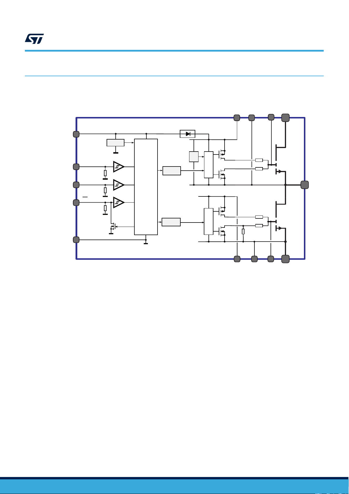
1 Block diagram
Driver
Driver
Logic,
interlocking,
overtemp
Level Shifter
Level Shifter
VCC UVLO
UVLO
Vbo
PGNDPVCC
OUTbBOOT
GL
GH
VCC
HIN
LIN
SD/OD
GND
OUT
VS
SENSE
HON
HOFF
LON
LOFF
R
BLEED
RGOFF
H
RGON
H
RGON
L
RGOFF
L
MASTERGAN3
Block diagram
Figure 1. MASTERGAN3 block diagram
DS13724 - Rev 1
page 2/30
Page 3
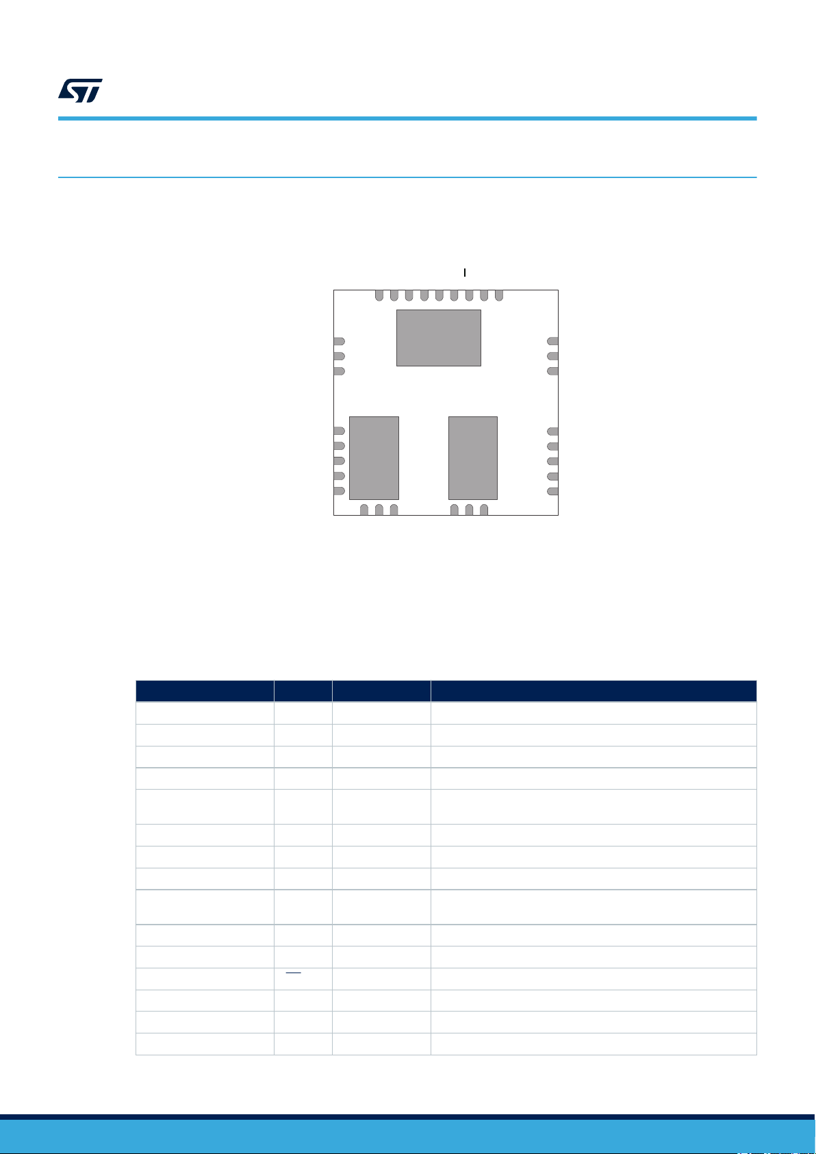
2 Pin description and connection diagram
1
2
3
4
5
6
7
8
9
10
11
12
13
14
15
24
23
22
21
20
19
18
17
16
31
30
29
28
27
26
25
GND
SENSE
OUT
EP1
EP2
EP3
SENSE
SENSE
SENSE
OUT
OUT
OUT
SENSE
SENSE
SENSE
SENSE
SENSE
VS
VS
VS
VS
VS
GH
OUTb
BOOT
PGND
GL
PVCC
N.C.
VCC
GND
LIN
HIN
SD/OD
N.C.
N.C.
N.C.
Figure 2. Pin connection (top view)
MASTERGAN3
Pin description and connection diagram
2.1 Pin list
Table 1. Pin description
Pin Number Pin Name Type Function
15, 16, 17, 18, 19 VS Power Supply High voltage supply (high-side GaN Drain)
12, 13, 14, EP3 OUT Power Output Half-bridge output
4, 5, 6, 7, 8, 9, 10, 11, EP2 SENSE Power Supply Half-bridge sense (low-side GaN Source)
22 BOOT Power Supply Gate driver high-side supply voltage
21 OUTb Power Supply
27 VCC Power Supply Logic supply voltage
1 PVCC Power Supply Gate driver low-side supply voltage
28, EP1 GND Power Supply Gate driver ground
3 PGND Power Supply
26 HIN Logic Input High-Side driver logic input
24 LIN Logic Input Low-Side driver logic input
25 SD/OD Logic Input-Output Driver Shutdown input and Fault Open-Drain
2 GL Output Low-Side GaN gate
20 GH Output High-Side GaN gate
23, 29, 30, 31 N.C. Not Connected Leave floating
Gate driver high-side reference voltage, used only for Bootstrap
capacitor connection. Internally connected to OUT.
Gate driver low-side buffer ground. Internally connected to
SENSE
DS13724 - Rev 1
page 3/30
Page 4
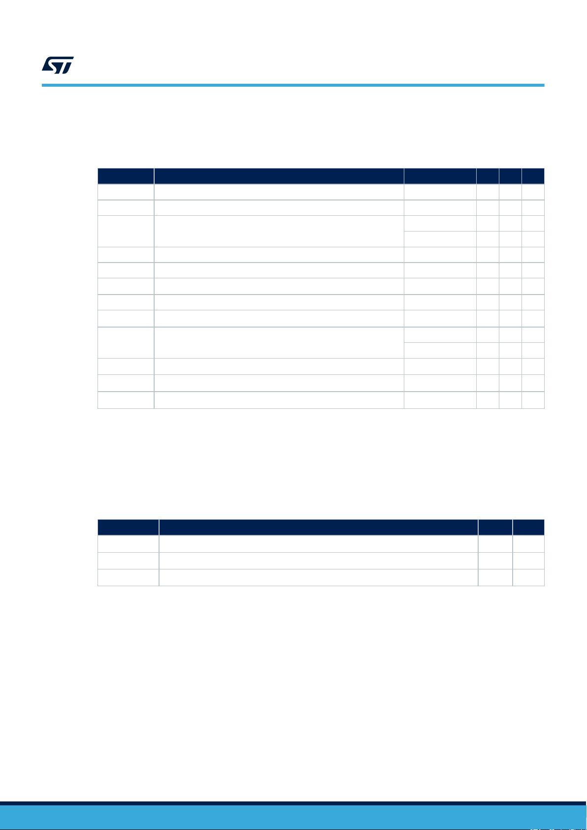
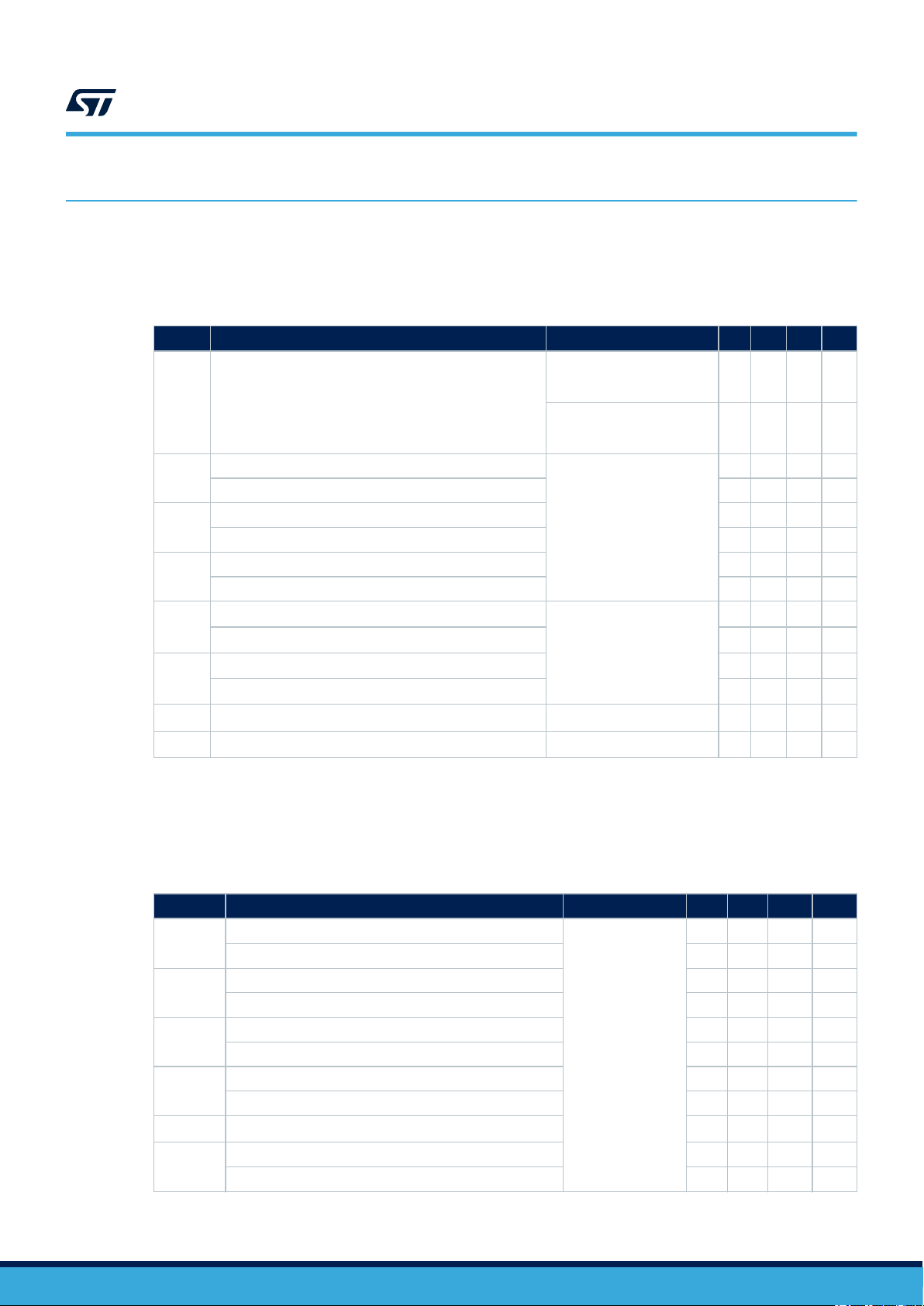
3 Electrical Data
3.1 Absolute maximum ratings
Each voltage referred to GND unless otherwise specified
Symbol Parameter Test Condition Value Unit
V
DS
VCC Logic supply voltage -0.3 to 11 V
PVCC-PGND
VCC-PGND Logic supply vs. Low-side driver ground -0.3 to 18.3 V
PVCC Low-side driver supply vs. logic ground -0.3 to 18.3 V
PGND Low-side driver ground vs. logic ground -7.3 to 11.3 V
V
BO
BOOT Bootstrap voltage -0.3 to 620 V
CGL, CGH
RGL, RGH
I
D
I
D
SR
V
T
T
1. PGND internally connected to SENSE
2. OUTb internally connected to OUT
3.
CGx < 0.08/(Pvcc^2*Fsw)-(330*10
4. TCB is temperature of case exposed pad.
5. Range estimated by characterization, not tested in production.
6. Value specified by design factor, pulse duration limited to 50 µs and junction temperature.
GaN Drain-to-Source Voltage
Low-side driver supply voltage
BOOT to OUTb voltage
(2)
Maximum external capacitance between GL and PGND and
between GH and OUTb
Minimum external pull-down resistance between GL and
PGND and GH and OUTb
Drain current (Low side GaN transistor)
Drain current (High side GaN transistor)
Half-bridge outputs slew rate (10% - 90%) 100 V/ns
out
Logic inputs voltage range -0.3 to 21 V
i
Junction temperature -40 to 150 °C
J
Storage temperature -40 to 150 °C
s
-12
)
Table 2. Absolute maximum ratings
(1)
DC @ TCB = 25°C
DC @ TCB = 100°C
Peak @ TCB = 25°C
DC @ TCB = 25°C
DC @ TCB = 100°C
Peak @ TCB = 25°C
TJ = 25 °C
Fsw = 500 kHz
MASTERGAN3
Electrical Data
620 V
-0.3 to 7 V
-0.3 to 7 V
(3)
(4) (5)
(4) (5)
(4) (5) (6)
(4) (5)
(4) (5)
(4) (5) (6)
3.9 nF
6.8 kΩ
6.5 A
4.4 A
12 A
4 A
2.6 A
7 A
DS13724 - Rev 1
page 4/30
Page 5
3.2 Recommended operating conditions
Table 3. Recommended operating conditions
Each voltage referred to GND unless otherwise specified
Symbol Parameter Note Min Max Unit
VS High voltage bus 0 520 V
VCC Supply voltage 4.75 9.5 V
PVCC-PGND
PVCC Low-side driver supply voltage 3 8.5 V
VCC-PVCC VCC to PVCC pin voltage -3 3 V
PGND
DT Suggested minimum deadtime 5 ns
T
IN_MIN
V
BO
BOOT BOOT to GND voltage
V
T
J
1. PGND internally connected to SENSE
2. OUTb internally connected to OUT
3. 5 V is recommended during high-hide turn-on
PVCC to PGND low side supply voltage
Low-side driver ground
(1)
Minimum duration of input pulse to obtain undistorted output pulse 120 ns
BOOT to OUTb pin voltage
Logic inputs voltage range 0 20 V
i
(2)
Junction temperature -40 125 °C
MASTERGAN3
Recommended operating conditions
(1)
Best performance 5 6.5 V
Best performance 5 6.5 V
4.75 6.5 V
-2 2 V
4.4 6.5 V
(3)
530 V
0
3.3
Thermal data
Table 4. Thermal data
Symbol Parameter Value Unit
R
th(J-CB)_LS
R
th(J-CB)_HS
R
th(J-A)
1. The junction to ambient thermal resistance is obtained simulating the device mounted on a 2s2p (4 layer) FR4 board as
JESD51-5,7 with 6 thermal vias for each exposed pad. Power dissipation uniformly distributed over the two GaN transistors.
Thermal resistance Low side junction to SENSE exposed pad, typical 2.8 °C/W
Thermal resistance High side junction to OUT exposed pad, typical 4.7 °C/W
Thermal resistance junction-to-ambient
(1)
18.8 °C/W
DS13724 - Rev 1
page 5/30
Page 6
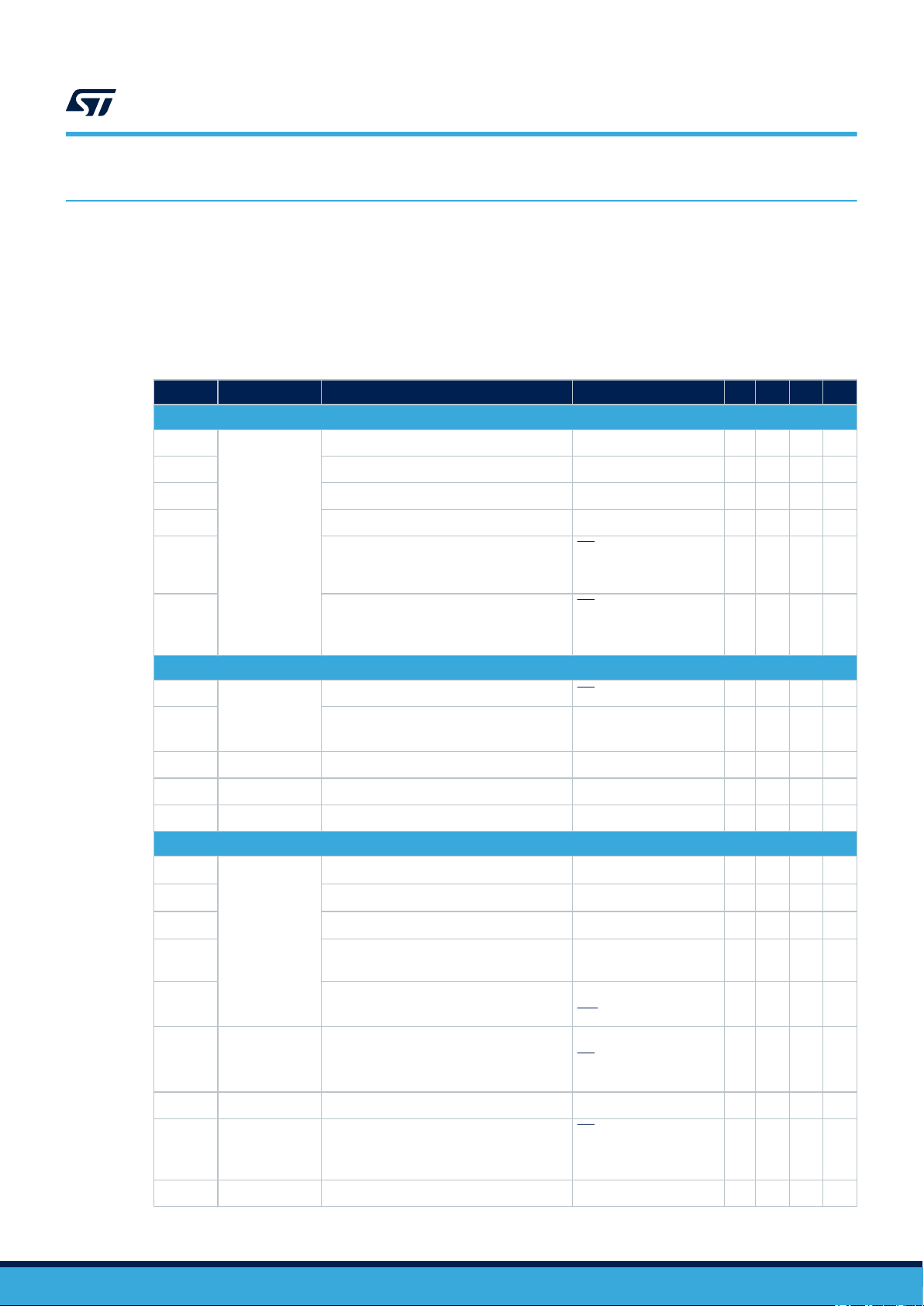
4 Electrical characteristics
4.1 Driver
Table 5. Driver electrical characteristics
VCC = PVCC = 6 V; SENSE = GND; TJ = 25°C, unless otherwise specified (each voltage referred to GND unless otherwise
specified)
Symbol Parameter Test condition Min Typ Max Unit
VCC
VCC
VCC
I
QVCCU
I
I
thON
thOFF
hys
VCC vs. GND
QVCC
SVCC
VCC UV turn ON threshold
VCC UV turn OFF threshold
VCC UV hysteresis
VCC undervoltage quiescent supply current VCC = PVCC = 3.8 V 320 410 μA
VCC quiescent supply current
VCC switching supply current
Logic section supply
(1)
(1)
(1)
SD/OD = LIN = 5 V;
HIN = 0 V;
BOOT = 7 V
SD/OD = 5 V;
VBO = 6.5 V;
VS = 0 V; FSW = 500 kHz
MASTERGAN3
Electrical characteristics
4.2 4.5 4.75 V
3.9 4.2 4.5 V
0.2 0.3 0.45 V
680 900 μA
0.8 mA
I
QPVCC
I
SPVCC
R
BLEED
RON
ROFF
V
BOthON
V
BOthOFF
V
BOhys
I
QBOU
I
QBO
I
SBO
I
LK
R
DBoot
RON
Low-side driver section supply
PVCC quiescent supply current SD/OD = LIN = 5 V 150 μA
PVCC vs. PGND
PVCC switching supply current
VS = 0 V
FSW = 500 kHz
1 mA
GL vs. PGND Low side gate bleeder PVCC = PGND 75 100 125 kΩ
L
L
Low side turn on resistance
Low side turn off resistance
(2)
(2)
I(GL) = 1 mA (source) 77 Ω
I(GL) = 1 mA (sink) 2 Ω
High-side floating section supply
(3)
(3)
(3)
VBO = 3.4 V
(3)
VBO = 6 V; LIN = GND;
SD/OD = HIN = 5 V;
3.6 4.0 4.4 V
3.4 3.7 4.0 V
0.1 0.3 0.5 V
140 200 μA
180 μA
BOOT vs. OUTb
VBO UV turn ON threshold
VBO UV turn OFF threshold
VBO UV hysteresis
VBO undervoltage quiescent supply
(3)
current
VBO quiescent supply current
VBO = 6 V;
BOOT BOOT switching supply current
SD/OD = 5 V;
1.1 mA
VS = 0 V; FSW = 500 kHz
BOOT vs. SGND High voltage leakage current BOOT = OUT = 600 V 11 μA
SD/OD = LIN = 5 V;
VCC vs. BOOT
Bootstrap diode on resistance
(4)
HIN = GND = PGND
140 175 Ω
VCC – BOOT = 0.5 V
H
High side turn on resistance
(2)
I(GH) = 1 mA (source) 77 Ω
DS13724 - Rev 1
page 6/30
Page 7
MASTERGAN3
Symbol Parameter Test condition Min Typ Max Unit
ROFF
V
V
V
ihys
I
INh
I
R
PD_IN
I
SDh
I
SDl
R
PD_SD
V
TSD
R
ON_OD
I
OL_OD
T
d,GL
T
d,GH
H
il
ih
INl
LIN, HIN, SD/OD
LIN, HIN
SD/OD Logic “1” input bias current SD/OD = 5 V 11 15 20 μA
SD/OD Logic “0” input bias current SD/OD = 0 V 1 μA
SD/OD Pull-down resistor
SD/OD Thermal shutdown unlatch threshold
SD/OD Open drain ON resistance
SD/OD Open Drain low level sink current
LIN, GL Prop. delay from LIN to GL
HIN, GH Prop. delay from HIN to GH
High side turn off resistance
Low level logic threshold
High level logic threshold
Logic input threshold hysteresis 0.7 0.96 1.2 V
Logic ‘1’ input bias current LIN, HIN = 5 V 23 33 55 μA
Logic ‘0’ input bias current LIN, HIN = GND 1 μA
Input pull-down resistor LIN, HIN = 5 V 90 150 220 kΩ
Overtemperature protection
T
TSD
T
HYS
Shutdown temperature
Temperature hysteresis
1. VCC UVLO is referred to VCC - GND
2. Turn on and turn off total resistances include the values of the gate resistors and the driver Rdson
3. VBO = V
4. R
BD(on)
R
BD(on)
Where: Ia is BOOT pin current when V
- V
BOOT
OUT
is tested in the following way:
= [(VCC - V
BOOTa
) - (VCC - V
BOOTb
BOOT
)] / [Ia - Ib]
= V
5. Range estimated by characterization, not tested in production.
6. Tested at wafer level.
(2)
Logic inputs
; Ib is BOOT pin current when V
BOOTa
I(GH) = 1 mA (sink) 2 Ω
TJ = 25°C
Full Temperature range
TJ = 25°C
Full Temperature range
SD/OD = 5 V
OpenDrain OFF
TJ = 25°C
(6)
TJ = 25°C;
I
OD
= 400 mV
(6)
TJ = 25°C;
VOD = 400 mV
(6)
(6)
(5)
(5)
(6)
BOOT
= V
1.1 1.31 1.45
(5)
0.8
2 2.17 2.5
(5)
250 330 450 kΩ
0.5 0.75 1 V
8 10 18 Ω
22 40 50 mA
175 °C
BOOTb
2.7
46 ns
46 ns
20 °C
Driver
V
V
DS13724 - Rev 1
page 7/30
Page 8
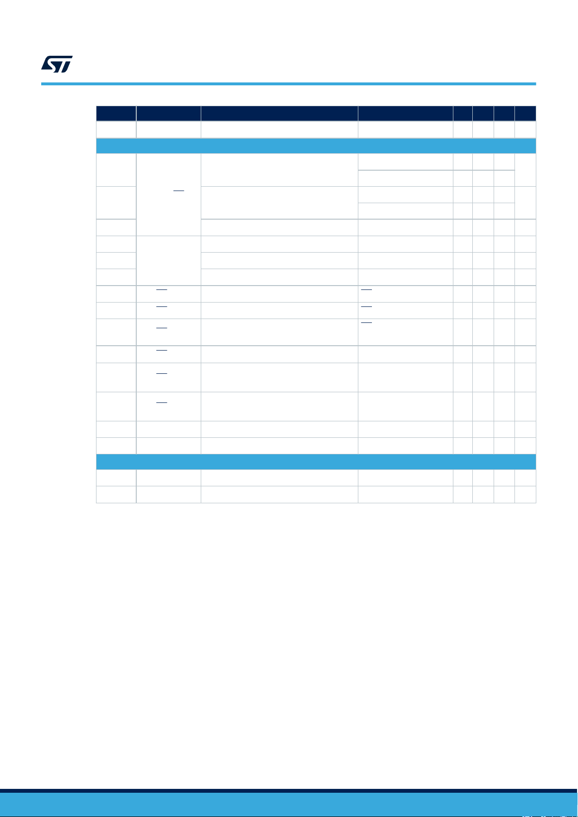
4.2 GaN power transistor
Table 6. GaN power transistor electrical characteristics
V
= 6 V; TJ = 25°C, unless otherwise specified
GS
Symbol Parameter Test condition Min Typ Max Unit
V
(BR)DS
Drain-source blocking voltage
GaN on/off states
Low side I
High side I
VGS = 0 V
< 13.3 µA
DSS
< 6.6 µA
DSS
MASTERGAN3
GaN power transistor
(1)
(1)
650 V
I
I
R
DS(on)_LS
R
DS(on)_HS
DSS_LS
DSS_HS
V
GS(th)
I
GS_LS
I
GS_HS
Zero gate voltage drain current - low side
Zero gate voltage drain current - high side
Gate threshold voltage
Gate to source current - Low side
Gate to source current - High side
Static drain-source on-resistance - Low side
Static drain-source on-resistance - High side
1. Tested at wafer level.
2. Value estimated by characterization, not tested in production.
VDS = 600 V
VGS = 0 V
VDS = 600 V
VGS = 0 V
VDS = V
GS
Low side, ID = 2.5 mA
High side, ID = 1.7 mA
VDS = 0 V
VDS = 0 V
(2)
(2)
TJ = 25°C
ID = 2.2 A
TJ = 125°C
TJ = 25°C
ID = 1.2 A
TJ = 125°C
0.5 µA
0.3 µA
(1)
(1)
1.7 V
40 µA
20 µA
225 300
(2)
495
mΩ
450 600
(2)
1012
mΩ
DS13724 - Rev 1
page 8/30
Page 9
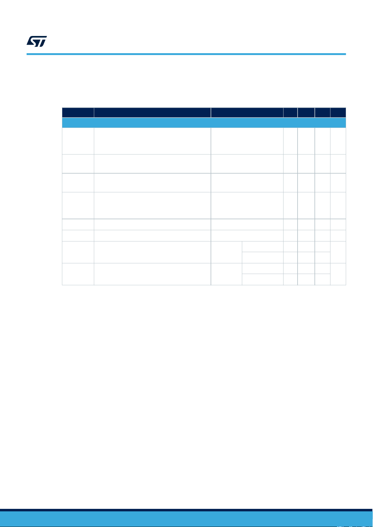
5 Device characterization values
The information in Table 7 and Table 8 represents typical values based on characterization and simulation results
and are not subject to the production test.
Table 7. GaN power transistor characterization values
Symbol Parameter Test condition Min Typ Max Unit
Q
Total gate charge
G
Device characterization values
VGS = 6 V, TJ = 25°C
VDS = 0 to 400 V - Low side
VGS = 6 V, TJ = 25°C
VDS = 0 to 400 V - High side
MASTERGAN3
1.5 nC
0.8 nC
Q
E
C
C
O(ER)
C
Q
I
RRM
1. C
2. C
Symbol
t
t
C(on)
t(off)
t
C(off)
Output charge - Low side
OSS
Output charge - High side 7 nC
Output capacitance stored energy - Low side 1.7 µJ
OSS
Output capacitance stored energy - High side 0.9 µJ
VGS = 0 V,
VDS = 400 V
Output capacitance - Low side 14.2 pF
OSS
Output capacitance - High side 7 pF
Effective output capacitance energy related - Low side
Effective output capacitance energy related - High side
Effective output capacitance time related - Low side
O(TR)
Effective output capacitance time related - High side
Reverse recovery charge 0 nC
RR
(1)
(1)
(2)
(2)
V
= 0 V,
GS
VDS = 0 to 400 V
Reverse recovery current 0 A
is the fixed capacitance that would give the same stored energy as C
O(ER)
V
DS
is the fixed capacitance that would give the same charging time as C
O(TR)
V
DS
while VDS is rising from 0 V to the stated
OSS
while VDS is rising from 0 V to the stated
OSS
Table 8. Inductive load switching characteristics
Parameter Test condition Min Typ Max Unit
(on)
t
E
Turn-on time - Low side
(1)
Turn-on time - High side 70 ns
Crossover time (on) - Low side 15 ns
(2)
Crossover time (on) - High side 25 ns
Turn-off time - Low side 70 ns
(1)
Turn-off time - High side 70 ns
Crossover time (off) - Low side 15 ns
(2)
Crossover time (off) - High side 10 ns
Shutdown to high/low-side propagation delay 70 ns
SD
VS = 400 V,
VGS = 6 V,
I
=2.2 A,
D_LS
I
=1.2 A
D_HS
See Figure 3
Turn-on switching losses - Low side 10 µJ
on
Turn-on switching losses - High side 4.5 µJ
70 ns
14 nC
21 pF
11 pF
34 pF
17 pF
DS13724 - Rev 1
page 9/30
Page 10

I
D
I
D
V
DS
V
DS
V
IN
V
IN
t
(ON)
t
(OFF)
t
C(ON)
t
C(OFF)
10%I
D
10%V
DS
10%I
D
10%V
DS
(a) turn-on
(b) turn-off
MASTERGAN3
Device characterization values
Symbol Parameter Test condition Min Typ Max Unit
VS = 400 V,
VGS = 6 V,
I
=2.2 A,
D_LS
I
=1.2 A
D_HS
See Figure 3
1. t
2. t
E
off
(on)
C(on)
Turn-off switching losses 2.5 µJ
and t
include the propagation delay time of the internal driver
(off)
and t
are the switching times of GaN transistor itself under the internally given gate driving conditions
C(off)
Figure 3. Switching time definition
DS13724 - Rev 1
page 10/30
Page 11

VDS (V)
I
D
(A)
VGS=6V
TJ=25°C
VGS=5V
0
1 2 3 4 5
0
2
4
6
8
10
12
14
16
18
20
VGS=4V
VDS (V)
I
D
(A)
VGS=6V
TJ=125°C
VGS=5V
0
1 2 3 4 5
0
1
2
3
4
5
6
7
8
9
10
VGS=4V
VDS (V)
I
D
(A)
VGS=6V
TJ=25°C
VGS=5V
0
1 2 3 4 5
0
1
2
3
4
5
6
7
8
9
10
VGS=4V
VDS (V)
I
D
(A)
VGS=6V
TJ=125°C
VGS=5V
0
1 2 3 4 5
0
0.5
1.0
1.5
2.0
2.5
3.0
3.5
4.0
4.5
5.0
VGS=4V
MASTERGAN3
Device characterization values
Figure 4. Typ I
vs. VDS at TJ=25°C
D_LS
Figure 5. Typ I
vs. VDS at TJ=125°C
D_LS
DS13724 - Rev 1
Figure 6. Typ I
vs. VDS at TJ=25°C
D_HS
Figure 7. Typ I
vs. VDS at TJ=125°C
D_HS
page 11/30
Page 12

0
2
10 18 20
0.22
0.24
0.26
0.28
0.30
0.32
0.34
0.36
0.38
TJ=25°C
ID (A)
R
DS(on)
(Ω)
4V
5V
6V
16
14124
86
0
1
5 9 10
0.45
0.48
0.51
0.54
0.57
0.60
0.63
0.66
0.69
TJ=125°C
ID (A)
R
DS(on)
(Ω)
4V
5V
6V
8
762
43
0
1
5 9 10
0.4
0.45
0.5
0.55
0.6
0.65
0.7
0.75
0.8
TJ=25°C
ID (A)
R
DS(on)
(Ω)
4V
5V
6V
8
762
43
0
0.5
2.5 4.5 5
0.8
0.9
1
1.1
1.2
1.3
1.4
1.5
1.6
TJ=125°C
ID (A)
R
DS(on)
(Ω)
4V
5V
6V
4
3.531
21.5
MASTERGAN3
Device characterization values
Figure 8. Typ R
Figure 10. Typ R
DS(on)_LS
DS(on)_HS
vs. ID at TJ=25°C
vs. ID at TJ=25°C
Figure 9. Typ R
Figure 11. Typ R
DS(on)_LS
DS(on)_HS
vs. ID at TJ=125°C
vs. ID at TJ=125°C
DS13724 - Rev 1
page 12/30
Page 13

VDS (V)
I
D
(A)
VGS=6V
TJ=25°C
0
1 2 3 4 5
0
2
4
6
8
10
12
14
16
18
20
TJ=50°C
TJ=75°C
TJ=100°C
TJ=125°C
VDS (V)
I
D
(A)
VGS=6V
TJ=25°C
0
1 2 3 4 5
0
1
2
3
4
5
6
7
8
9
10
TJ=50°C
TJ=75°C
TJ=100°C
TJ=125°C
Normalized R
DS(on)
(1 at 25°C)
0
1.0
0.5
1.5
2.0
2.5
3.0
Temperature (°C)
-50
-10
30
70
110
150
MASTERGAN3
Device characterization values
Figure 12. Typ I
vs. V
D_LS
DS
Figure 14. Typ R
vs. TJ normalized at 25°C
DS(on)
Figure 13. Typ I
D_HS
vs. V
DS
DS13724 - Rev 1
page 13/30
Page 14

VSD (V)
I
S
(A)
VGS=6V
TJ=25°C
VGS=0V
0
1 2 3 4 5 6 7 8 9 10
0
4
8
12
16
20
24
28
32
36
40
VSD (V)
I
S
(A)
VGS=6V
TJ=125°C
VGS=0V
0
1 2 3 4 5 6 7 8 9 10
0
2
4
6
8
10
12
14
16
18
20
VSD (V)
I
S
(A)
VGS=6V
TJ=25°C
VGS=0V
0
1 2 3 4 5 6 7 8 9 10
0
2
4
6
8
10
12
14
16
18
20
VSD (V)
I
S
(A)
VGS=6V
TJ=125°C
VGS=0V
0
1 2 3 4 5 6 7 8 9 10
0
1
2
3
4
5
6
7
8
9
10
MASTERGAN3
Device characterization values
Figure 15. Typ I
Figure 17. Typ I
SD_LS
SD_HS
vs. V
vs. V
SD_LS
SD_HS
at TJ=25°C
at TJ=25°C
Figure 16. Typ I
Figure 18. Typ I
SD_LS
SD_HS
vs. V
vs. V
SD_LS
SD_HS
at TJ=125°C
at TJ=125°C
DS13724 - Rev 1
page 14/30
Page 15

1
10
100
1000
0.01
0.1
1
10
DC
50 μs
0.2 μs
Id (A)
Vds (V)
1
10
100
1000
0.01
0.1
1
10
DC
50 μs
0.2 μs
Id (A)
Vds (V)
0 0.5
1
1.5
2
2.5
QG (nC)
V
GS
(V)
0
2
1
3
4
5
6
400 V
100 V
7
0 0.2
0.4
0.6
0.8
1
QG (nC)
V
GS
(V)
0
2
1
3
4
5
6
400 V
100 V
7
MASTERGAN3
Device characterization values
Figure 19. Safe Operating Area (LS) at TJ=25°C
Figure 21. Typical Gate Charge (LS) at TJ=25°C
Figure 20. Safe Operating Area (HS) at TJ=25°C
Figure 22. Typical Gate Charge (HS) at TJ=25°C
DS13724 - Rev 1
page 15/30
Page 16

0
25
50
75
100
125
TCB (°C)
0
150
10
20
30
40
50
60
70
P
DISS
(W)
0
25
50
75
100
125
TCB (°C)
0
150
5
10
15
20
25
30
35
P
DISS
(W)
R
DBoot
(ohm)
0
100
50
150
200
250
300
Temperature (°C)
-50
-10
30
70
110
150
MASTERGAN3
Device characterization values
Figure 23. LS Derating curve
Figure 25. Typ R
Dboot
Figure 24. HS Derating curve
vs. T
J
DS13724 - Rev 1
page 16/30
Page 17

6 Functional description
6.1 Logic inputs
The MASTERGAN3 features a half-bridge gate driver with three logic inputs to control the internal high-side and
low-side GaN transistors.
The devices are controlled through the following logic inputs:
• SD/OD: Shutdown input, active low
• LIN: low-side driver inputs, active high
• HIN: high-side driver inputs, active high
Table 9. Inputs truth table (applicable when device is not in UVLO)
Input pins GaN transistors status
SD/OD LIN HIN LS HS
L
H L L OFF OFF
H L H OFF ON
H H L ON OFF
1. X: Don’t care
2. Interlocking
H
(1)
X
(2)
H
MASTERGAN3
Functional description
(1)
X
(2)
H
OFF OFF
OFF OFF
The logic inputs have internal pull-down resistors. The purpose of these resistors is to set a proper logic level in
case, for example, there is an interruption in the logic lines or the controller outputs are in tri-state conditions.
If logic inputs are left floating, the gate driver outputs are set to low level and the correspondent GaN transistors
are turned off.
The minimum duration of the on time of the pulses applied to LIN is T
either extended to T
or blanked, when shorter than 30ns (typ).
IN_MIN
The minimum duration of the off time of the pulses applied to HIN is T
either extended to T
Interlocking feature interrupts running T
or blanked, when shorter than 30 ns (typ).
IN_MIN
to avoid unexpected cross-conduction.
IN_MIN
Matched, short propagation delay between low side and high side are there.
6.2
Bootstrap structure
A bootstrap circuitry is typically used to supply the high-voltage section. MASTERGAN3 integrates this structure,
realized by a patented integrated high-voltage DMOS, to reduce the external components.
The Boostrap integrated circuit is connected to VCC pin and is driven synchronously with the low-side driver.
The use of an external bootstrap diode in parallel to the integrated structure is possible, in particular if the
operating frequency is approximately higher than 500 kHz.
6.3 VCC supply pins and UVLO function
The VCC pin supplies current to the logic circuit, level-shifters in the low-side section and the integrated bootstrap
diode.
The PVCC pin supplies low-side output buffer. During output commutations the average current used to provide
gate charge to the high-side and low-side GaN transistors flows through this pin.
= 120 ns; shorter pulses shall be
IN_MIN
= 120 ns; shorter pulses shall be
IN_MIN
DS13724 - Rev 1
page 17/30
Page 18

VCC = PVCC
VCC
thON
VCC
thOFF
UVLO VCC
0V
0V
VCC rise
Tdelay_VCC
Tdelay_VCC
LIN
GL-PGND
0V
PVCC
MASTERGAN3
VBO UVLO protection
The PVCC pin can be connected either to the same supply voltage of the VCC pin or to a separate voltage
source. In case the same voltage source is used, it is suggested to connect VCC and PVCC pins by means of
a small decoupling resistance. The use of dedicated bypass ceramic capacitors located as close as possible to
each supply pin is highly recommended.
The MASTERGAN3 VCC supply voltage is continuously monitored by under-voltage lockout (UVLO) circuitry that
turns both the high-side and low-side GaN transistors off when the supply voltage goes below the V
threshold. The UVLO circuitry turns on the GaN, according to LIN and HIN status, approximately 20 µs (typ) after
the supply voltage goes above the V
CCthON
voltage. A V
hysteresis is provided for noise rejection purposes.
CChys
Figure 26. VCC UVLO and Low Side
CC_thOFF
6.4
VBO UVLO protection
Dedicated undervoltage protection is available on the bootstrap section between BOOT and OUTb supply pins. In
order to avoid intermittent operation, a hysteresis sets the turn-off threshold with respect to the turn-on threshold.
Approximately 5 µs (typ) after VBO voltage falls below V
switched off. When VBO voltage reaches the V
BOthON
BOthOFF
threshold, the device returns to normal operation and the
output remains off until the next input pin transition that requests the high-side to turn on.
threshold, the high-side GaN transistor is
DS13724 - Rev 1
page 18/30
Page 19

Figure 27. VBO UVLO and High Side
VCC
VCCthON
VCCthOFF
HIN
UVLO VBO
0V
0V
VBOrise
(GH-OUTB)
VBO
0V
V
BOthON
VBOthOFF
0V
VBO
MASTERGAN3
Thermal shutdown
6.5 Thermal shutdown
The integrated gate driver has a thermal shutdown protection.
When junction temperature reaches the T
leaving the half-bridge in 3-state and signaling the state forcing
junction temperature is below T
GaN are driven again according to inputs when
The thermal smart shutdown system provides the possibility to increase the time constant of the external RC
network (that determines the disable time after the overtemperature event) up to very large values without
delaying the protection.
TSD-THYS
temperature threshold, the device turns off both GaN transistors,
TSD
SD/OD pin low. SD/OD pin is released when
and SD/OD is below V
TSD
.
SD/OD rises above Vih.
DS13724 - Rev 1
page 19/30
Page 20

Figure 28. Thermal shutdown timing waveform
THERMAL SHUTDOWN CIRCUIT
GH/GL
OD gate
(internal)
Fast shut down
the driver outputs are switched off
disable time
SD/OD
T
TSDTHYSTTSD -
VihV
0 V
TSDVOD
TJ
t1t
2
VPU
SD/OD
FROM / TO
CONTROLLER
C
OD
THERMAL
SHUTDOWN
LOGIC
R
ON_ODRPD_SD
R
OD_ext
2
1
immediately after overtemperature
MASTERGAN3
Thermal shutdown
DS13724 - Rev 1
page 20/30
Page 21

7 Typical application diagrams
+
C
PVCC
FROM/TO CONTROLLER
H.V.
C
R
CBOOT
CVCC
C
R
COD
R
VOUT
VCC
VCC
VPU
CC
CbuS
FROM/TO CONTROLLER
FROM/TO CONTROLLER
TO CONTROLLER
Driver
Driver
Logic,
interlocking,
overtemp
Level Shifter
Level Shifter
VCC UVLO
UVLO
Vbo
PGNDPVCC
OUTbBOOT
GL
GH
VCC
HIN
LIN
SD/OD
GND
OUT
VS
SENSE
HON
HOFF
LON
LOFF
R
BLEED
RON
L
ROFF
L
ROFF
H
RON
H
Figure 29. Asymmetrical Active clamp flyback
MASTERGAN3
Typical application diagrams
DS13724 - Rev 1
page 21/30
Page 22

8 Package information
In order to meet environmental requirements, ST offers these devices in different grades of ECOPACK packages,
depending on their level of environmental compliance. ECOPACK specifications, grade definitions and product
status are available at: www.st.com. ECOPACK is an ST trademark.
8.1 QFN 9 x 9 x 1 mm, 31 leads, pitch 0.6 mm package information
Table 10. QFN 9 x 9 x 1 mm package dimensions
MASTERGAN3
Package information
Symbol
A
A3 0.10
b 0.25 0.30 0.35
D 8.96 9.00 9.04
E 8.96 9.00 9.04
D1 3.30 3.40 3.50
E1 2.06 2.16 2.26
D2 1.76 1.86 1.96
E2 3.10 3.20 3.30
D3 1.70 1.80 1.90
E3 3.10 3.20 3.30
e 0.60
K 0.24
L 0.35 0.45 0.55
N 31
aaa 0.10
bbb 0.10
ccc 0.10
ddd 0.05
eee 0.08
Min. Typ. Max.
0.90 0.95 1.00
Dimensions (mm)
Note: 1. Dimensioning and tolerances conform to ASME Y14.5-2009.
2. All dimensions are in millimeters.
3. N total number of terminals.
4. Dimensions do not include mold protrusion, not to exceed 0.15 mm.
5. Package outline exclusive of metal burr dimensions.
DS13724 - Rev 1
page 22/30
Page 23

Figure 30. QFN 9 x 9 x 1 mm package dimensions
TOP VIEW
SIDE
VIEW
BOTTOM VIEW
MASTERGAN3
QFN 9 x 9 x 1 mm, 31 leads, pitch 0.6 mm package information
DS13724 - Rev 1
page 23/30
Page 24

9 Suggested footprint
TOP VIEW
Dimensions in mm
The MASTERGAN3 footprint for the PCB layout is usually defined based on several design factors such as
assembly plant technology capabilities and board component density. For easy device usage and evaluation, ST
provides the following footprint design, which is suitable for the largest variety of PCBs.
The following footprint indicates the copper area that should be free of solder mask, and shall extend beyond the
indicated areas, especially for EP2 and EP3. To aid thermal dissipation, it is recommended to add thermal vias
under these EPADs to transfer and dissipate device heat to the other PCB copper layers. A PCB layout example
is available with the MASTERGAN3 evaluation board.
Figure 31. Suggested footprint (top view drawing)
MASTERGAN3
Suggested footprint
DS13724 - Rev 1
page 24/30
Page 25

10 Ordering information
Order code Package Package Marking Packaging
MASTERGAN3 QFN 9 x 9 x 1 mm MASTERGAN3 Tray
MASTERGAN3TR QFN 9 x 9 x 1 mm MASTERGAN3 Tape and Reel
MASTERGAN3
Ordering information
Table 11. Order codes
DS13724 - Rev 1
page 25/30
Page 26

Revision history
MASTERGAN3
Table 12. Document revision history
Date Version Changes
07-May-2021 1 Initial release.
DS13724 - Rev 1
page 26/30
Page 27

MASTERGAN3
Contents
Contents
1 Block diagram .....................................................................2
2 Pin description and connection diagram ...........................................3
2.1 Pin list ........................................................................3
3 Electrical Data .....................................................................4
3.1 Absolute maximum ratings.......................................................4
3.2 Recommended operating conditions ..............................................5
3.3 Thermal data ..................................................................5
4 Electrical characteristics...........................................................6
4.1 Driver ........................................................................6
4.2 GaN power transistor ...........................................................8
5 Device characterization values.....................................................9
6 Functional description ............................................................17
6.1 Logic inputs ..................................................................17
6.2 Bootstrap structure ............................................................17
6.3 VCC supply pins and UVLO function .............................................17
6.4 VBO UVLO protection ..........................................................18
6.5 Thermal shutdown.............................................................19
7 Typical application diagrams......................................................21
8 Package information..............................................................22
8.1 [Package name] package information ............................................22
9 Suggested footprint ..............................................................24
10 Ordering information .............................................................25
Revision history .......................................................................26
Contents ..............................................................................27
List of tables ..........................................................................28
List of figures..........................................................................29
DS13724 - Rev 1
page 27/30
Page 28

MASTERGAN3
List of tables
List of tables
Table 1. Pin description......................................................................3
Table 2. Absolute maximum ratings .............................................................4
Table 3. Recommended operating conditions....................................................... 5
Table 4. Thermal data.......................................................................5
Table 5. Driver electrical characteristics ..........................................................6
Table 6. GaN power transistor electrical characteristics................................................ 8
Table 7. GaN power transistor characterization values ................................................9
Table 8. Inductive load switching characteristics.....................................................9
Table 9. Inputs truth table (applicable when device is not in UVLO)....................................... 17
Table 10. QFN 9 x 9 x 1 mm package dimensions ................................................... 22
Table 11. Order codes ...................................................................... 25
Table 12. Document revision history ............................................................. 26
DS13724 - Rev 1
page 28/30
Page 29

MASTERGAN3
List of figures
List of figures
Figure 1. MASTERGAN3 block diagram .........................................................2
Figure 2. Pin connection (top view) .............................................................3
Figure 3. Switching time definition ............................................................ 10
Figure 4. Typ I
Figure 5. Typ I
Figure 6. Typ I
Figure 7. Typ I
Figure 8. Typ R
Figure 9. Typ R
Figure 10. Typ R
Figure 11. Typ R
Figure 12. Typ I
Figure 13. Typ I
Figure 14. Typ R
Figure 15. Typ I
Figure 16. Typ I
Figure 17. Typ I
Figure 18. Typ I
Figure 19. Safe Operating Area (LS) at TJ=25°C ................................................... 15
Figure 20. Safe Operating Area (HS) at TJ=25°C ................................................... 15
Figure 21. Typical Gate Charge (LS) at TJ=25°C ................................................... 15
Figure 22. Typical Gate Charge (HS) at TJ=25°C ................................................... 15
Figure 23. LS Derating curve .................................................................16
Figure 24. HS Derating curve................................................................. 16
Figure 25. Typ R
Figure 26. VCC UVLO and Low Side ........................................................... 18
Figure 27. VBO UVLO and High Side ........................................................... 19
Figure 28. Thermal shutdown timing waveform .................................................... 20
Figure 29. Asymmetrical Active clamp flyback ..................................................... 21
Figure 30. QFN 9 x 9 x 1 mm package dimensions .................................................. 23
Figure 31. Suggested footprint (top view drawing) .................................................. 24
vs. VDS at TJ=25°C ......................................................... 11
D_LS
vs. VDS at TJ=125°C ........................................................ 11
D_LS
vs. VDS at TJ=25°C......................................................... 11
D_HS
vs. VDS at TJ=125°C ........................................................ 11
D_HS
DS(on)_LS
DS(on)_LS
DS(on)_HS
DS(on)_HS
D_LS
D_HS
DS(on)
SD_LS
SD_LS
SD_HS
SD_HS
Dboot
vs. ID at TJ=25°C....................................................... 12
vs. ID at TJ=125°C ...................................................... 12
vs. ID at TJ=25°C ...................................................... 12
vs. ID at TJ=125°C ..................................................... 12
vs. VDS ................................................................. 13
vs. VDS ................................................................ 13
vs. TJ normalized at 25°C ...................................................13
vs. V
vs. V
vs. V
vs. V
at TJ=25°C ...................................................... 14
SD_LS
at TJ=125°C .....................................................14
SD_LS
at TJ=25°C ..................................................... 14
SD_HS
at TJ=125°C .................................................... 14
SD_HS
vs. TJ ................................................................. 16
DS13724 - Rev 1
page 29/30
Page 30

MASTERGAN3
IMPORTANT NOTICE – PLEASE READ CAREFULLY
STMicroelectronics NV and its subsidiaries (“ST”) reserve the right to make changes, corrections, enhancements, modifications, and improvements to ST
products and/or to this document at any time without notice. Purchasers should obtain the latest relevant information on ST products before placing orders. ST
products are sold pursuant to ST’s terms and conditions of sale in place at the time of order acknowledgement.
Purchasers are solely responsible for the choice, selection, and use of ST products and ST assumes no liability for application assistance or the design of
Purchasers’ products.
No license, express or implied, to any intellectual property right is granted by ST herein.
Resale of ST products with provisions different from the information set forth herein shall void any warranty granted by ST for such product.
ST and the ST logo are trademarks of ST. For additional information about ST trademarks, please refer to www.st.com/trademarks. All other product or service
names are the property of their respective owners.
Information in this document supersedes and replaces information previously supplied in any prior versions of this document.
© 2021 STMicroelectronics – All rights reserved
DS13724 - Rev 1
page 30/30
 Loading...